
Semiconductor Ceramic Packaging Materials Market Size and Share
Market Overview
| Study Period | 2022 - 2032 |
|---|---|
| Market Size (2027) | USD 2.17 Billion |
| Market Size (2032) | USD 3.26 Billion |
| Growth Rate (2027 - 2032) | 8.46 % |
| Fastest Growing Market | Asia-Pacific |
| Largest Market | Asia-Pacific |
| Market Concentration | Low |
Major Players *Disclaimer: Major Players sorted in no particular order Image © Mordor Intelligence. Reuse requires attribution under CC BY 4.0. | |
Semiconductor Ceramic Packaging Materials Market Analysis by Mordor Intelligence
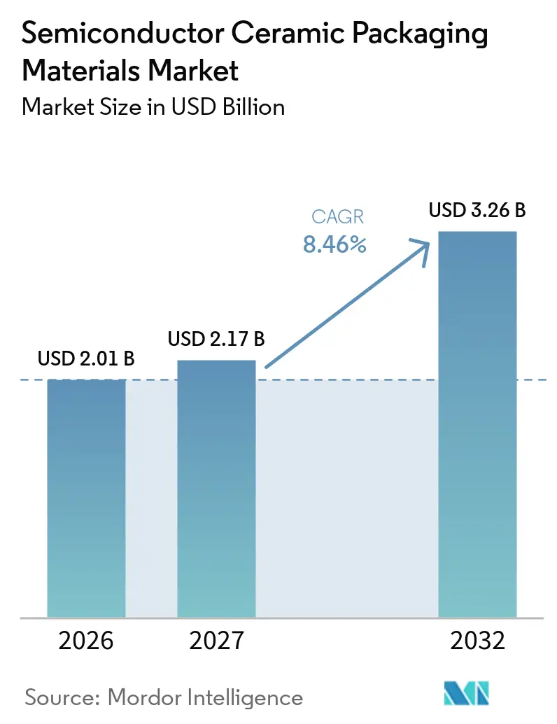
The semiconductor ceramic packaging materials market size was valued at USD 2.01 billion in 2026 and is estimated to grow from USD 2.17 billion in 2027 to reach USD 3.26 billion by 2032, at a CAGR of 8.46% during the forecast period (2027-2032). Ceramic packaging remains important where semiconductor devices need electrical isolation, hermetic sealing, and effective heat transfer at the same time. Higher power densities in artificial intelligence accelerators, radio-frequency modules, and vehicle power electronics are making thermal performance a material-selection requirement rather than a secondary feature. The semiconductor ceramic packaging materials market is supported by demand from advanced packaging, high-frequency communications, and electric vehicles, while its higher processing cost limits use in less demanding applications. Suppliers are responding with capacity additions, smaller package formats, and substrate designs that address warpage and heat-management needs in data centers and power modules.
Key Report Takeaways
- By material, alumina held 45.34% of the semiconductor ceramic packaging materials market share in 2026, while aluminum nitride is forecast to advance at an 8.85% CAGR through 2032.
- By packaging technology, surface mount packages - leadless, held 34.12% of the semiconductor ceramic packaging materials market share in 2026 and are forecast to advance at a 9.23% CAGR through 2032.
- By end-use industry, consumer electronics held 31.75% of the semiconductor ceramic packaging materials market share in 2026, while automotive is forecast to advance at a 9.67% CAGR through 2032.
- By geography, Asia-Pacific held 42.58% of the semiconductor ceramic packaging materials market share in 2026 and is forecast to advance at a 9.41% CAGR through 2032.
Note: Market numbers in this report are based on Mordor Intelligence's proprietary estimation framework, which combines nine months of actuals with Q4 projections for base year 2026.
Global Semiconductor Ceramic Packaging Materials Market Trends and Insights
Drivers Impact Analysis*
| Driver | (~) % Impact on CAGR Forecast | Geographic Relevance | Impact Timeline |
|---|---|---|---|
| Rising Semiconductor Device Complexity | +2.1% | Global | Short term (≤ 2 years) |
| Growth in 5G Infrastructure and RF Devices | +1.7% | APAC core, spillover to North America & EU | Medium term (2–4 years) |
| EV Power Modules and Wide-Bandgap Semiconductor Adoption | +1.5% | North America, EU, APAC core | Medium term (2–4 years) |
| AI Data Centers and High-Performance Computing Thermal Loads | +1.3% | North America & EU, APAC core | Short term (≤ 2 years) |
| Ceramic Package Demand from Heterogeneous Integration | +1.1% | Global | Long term (≥ 4 years) |
| Source: Mordor Intelligence | |||
Rising Semiconductor Device Complexity
Greater transistor density and three-dimensional die stacking increase heat flow within compact packages. Alumina, aluminum nitride, and silicon nitride retain a role in advanced designs because they combine electrical insulation, thermal conductivity, and hermeticity. KYOCERA Corporation introduced a multilayer ceramic core substrate in 2026 with 75 µm vias at a 200 µm pitch for xPU and switch application-specific integrated circuit packages. Such dimensions support denser routing in package structures where organic substrates face warpage constraints. High-temperature co-fired ceramic and low-temperature co-fired ceramic processes also allow multilayer routing and embedded functions within a ceramic body, which strengthens the semiconductor ceramic packaging materials market.
Growth in 5G Infrastructure and RF Devices
Fifth-generation network equipment needs amplifiers and filter assemblies that remain stable at elevated operating temperatures. A 2025 review identified low dielectric loss and a near-zero temperature coefficient of resonant frequency as important characteristics for microwave dielectric ceramics used in fifth-generation and sixth-generation communications hardware. These properties support the semiconductor ceramic packaging materials market, where radio-frequency performance and heat control are both important. Ceramic packages are relevant to power amplifiers, filters, and related components in network infrastructure and portable electronics. This creates demand across both infrastructure equipment and consumer devices, which broadens the customer base for ceramic materials.
EV Power Modules and Wide-Bandgap Semiconductor Adoption
Electric vehicle traction inverters using 800 V architectures require substrates that can withstand repeated thermal cycling. A 2025 Institute of Electrical and Electronics Engineers (IEEE) study found that the reliability of silicon carbide metal-oxide-semiconductor field-effect transistor modules was linked to substrate thermal-cycling life. The study reported that silicon nitride substrates lasted at least 3.5 times longer than alumina in the standardized tests discussed. Wide-bandgap devices increase the need to match the thermal and coefficient-of-thermal-expansion properties of the semiconductor and substrate. As vehicle platforms move to higher-voltage powertrains, qualification standards make material reliability more influential in the semiconductor ceramic packaging materials market.
AI Data Centers and High-Performance Computing Thermal Loads
Artificial intelligence accelerators can draw 700 W to 1,000 W per device, increasing the importance of package-level thermal management. In June 2025, Coherent Corp. released a diamond-loaded silicon carbide ceramic composite designed for direct liquid cooling and microchannel cold plates. A 2025 study also evaluated low-temperature co-fired ceramic liquid cold plates for high-performance computing processors. KYOCERA Corporation positioned its 2026 multilayer ceramic core substrate for artificial intelligence packages, where large organic substrates can warp. The semiconductor ceramic packaging materials market, therefore, benefits when thermal control becomes integral to the package design rather than an external system requirement.
Restraints Impact Analysis*
| Restraint | (~) % Impact on CAGR Forecast | Geographic Relevance | Impact Timeline |
|---|---|---|---|
| High Processing and Precision Machining Costs | -0.9% | Global | Short term (≤ 2 years) |
| Competition from Organic and Polymer Substrates | -0.7% | North America & EU | Medium term (2–4 years) |
| Thermal-Expansion Mismatch at Ceramic-Metal Interfaces | -0.5% | Global | Long term (≥ 4 years) |
| Source: Mordor Intelligence | |||
High Processing and Precision Machining Costs
Ceramic packages require high-temperature sintering, green-sheet lamination, and controlled co-firing processes. These production steps increase cost relative to standard organic boards and make ceramic solutions less suitable for every electronics design. The cost difference is most important in consumer electronics, where high production volumes place strong pressure on component pricing. Ceramic-metal interfaces can also face a coefficient-of-thermal-expansion mismatch during demanding thermal cycles. Manufacturers in the semiconductor ceramic packaging materials market must balance package reliability, machining yield, and material cost when they select substrate configurations.
Competition from Organic and Polymer Substrates
Organic substrates remain common in mainstream semiconductor packaging because established printed circuit board lines can produce them at high volume. Onto Innovation reported in 2025 that advanced organic substrate technologies are moving toward sub-2 µm line-space redistribution layers. These improvements reduce the performance gap in applications with moderate thermal requirements. Glass-core designs are also being evaluated for advanced packages because they offer flatness and dielectric characteristics that can address some packaging requirements. The semiconductor ceramic packaging materials market retains its clearest advantage in designs that require high thermal performance, robust insulation, or hermetic sealing.
*Our forecasts treat driver/restraint impacts as directional, not additive. The impact forecasts reflect baseline growth, mix effects, and variable interactions.
Segment Analysis
By Material: Alumina Supports Revenue Demand While Aluminum Nitride Serves Higher-Thermal Applications
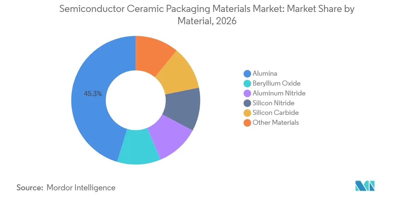
Alumina held 45.34% of the semiconductor ceramic packaging materials market size in 2026. Its established supply chain and cost-to-performance profile support use in consumer electronics, standard integrated circuit packages, and radio-frequency filters within the semiconductor ceramic packaging materials market. A 2025 review described ongoing work on filler morphology and surface modification in alumina-based electronic packaging composites. These developments help retain alumina’s relevance where suppliers need incremental performance improvements without moving to a higher-cost material. Silicon nitride and silicon carbide serve more specialized requirements in power modules and harsh operating conditions.
Aluminum nitride is projected to advance at an 8.85% CAGR through 2032. In the semiconductor ceramic packaging materials market, it is suited to electric vehicle inverters, fifth-generation base-station amplifiers, and liquid-cooled server assemblies because thermal performance is a central requirement in these uses. Research published in 2025 reported aluminum nitride films with thermal conductivity of 191 W m⁻¹ K⁻¹. NGK Corporation announced in November 2025 that it would triple the capacity for its HICERAM Carrier translucent alumina wafer by fiscal 2027.

By Packaging Technology: Surface Mount Packages – Leadless Combine Scale and Growth
Surface mount packages - leadless held 34.12% of the semiconductor ceramic packaging materials market size in 2026 and are projected to advance at a 9.23% CAGR through 2032. Their compact design reduces parasitic inductance and supports smaller board footprints. These features matter in fifth-generation radio-frequency modules, microelectromechanical systems sensors, and Internet of Things devices. KYOCERA Corporation displayed a smaller leadless ceramic package for microelectromechanical systems applications at the European Microelectronics and Packaging Conference in 2025. The company identified automotive advanced driver-assistance systems and wearables as relevant applications.
Leaded surface-mount packages continue to serve mid-power consumer and industrial equipment, where lead formability assists repair processes. Through-hole packages also remain relevant in harsh-environment defense and high-power designs. Advanced miniaturized packages are associated with emerging imaging and sensor applications. Other formats include wafer-level ceramic packaging and embedded chip-in-ceramic architectures for silicon photonics and co-packaged optics. In March 2026, KYOCERA Corporation exhibited ceramic solutions for co-packaged optics and silicon photonics at the Optical Fiber Communication Conference, extending its position in the semiconductor ceramic packaging materials market.
By End-Use Industry: Consumer Electronics Provides Scale While Automotive Increases Demand for Reliability
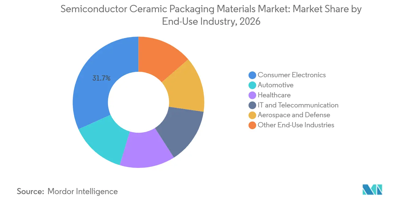
Consumer electronics held 31.75% of the semiconductor ceramic packaging materials market size in 2026. Smartphones, wearables, and augmented reality and extended reality headsets use ceramic packages in microelectromechanical systems, microphones, oscillators, radio-frequency filters, and image sensors. In July 2025, Murata Manufacturing Co., Ltd. began mass production of a 47 µF multilayer ceramic capacitor in the 0402-inch size. The company stated that the component reduced mounting area by 60% compared with the prior 0603-inch equivalent. This supports continued component miniaturization in portable electronics.
Automotive is projected to advance at a 9.67% CAGR through 2032. Silicon carbide metal-oxide-semiconductor field-effect transistor inverters in battery electric and plug-in hybrid vehicles require substrates that withstand repeated operation above 150 °C. Murata Manufacturing Co., Ltd. entered mass production of a 10 µF, 50 V DC multilayer ceramic capacitor in the 0805-inch size for automotive applications in June 2025. The company reported 2.1 times the capacitance of the prior generation in a 53% smaller package. Healthcare, aerospace and defense, industrial automation, and grid-edge energy conversion add demand for high-reliability ceramic packages.
Geography Analysis
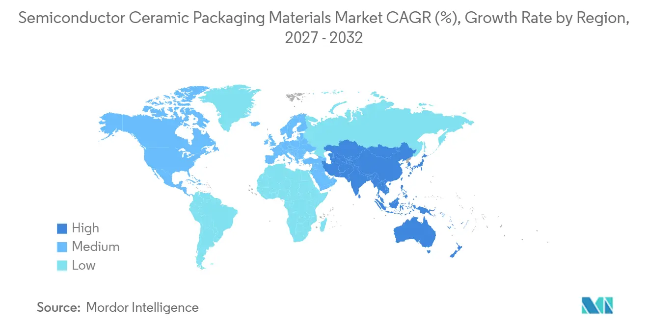
Asia-Pacific held 42.58% of the semiconductor ceramic packaging materials market share in 2026 and is projected to advance at a 9.41% CAGR through 2032. Japan, China, South Korea, and Taiwan combine advanced packaging capacity, integrated circuit design activity, and ceramic material production. In September 2026, KYOCERA Corporation completed its Nagasaki Isahaya Plant with a JPY 68 billion investment (approximately USD 453 million). The plant is intended to produce semiconductor packages for artificial intelligence data centers and electric vehicle applications, with a planned annual output of JPY 25 billion (approximately USD 167 million) from fiscal 2030. Murata Manufacturing Co., Ltd. also opened its first India manufacturing plant in Chennai in August 2025 for packaging and shipping multilayer ceramic capacitors.
North America accounts for a substantial share of demand through defense-grade hermetic packages, artificial intelligence data center substrates, and domestic chip-fabrication investment. A 2025 study of ceramic substrates for large-scale chiplet integration identified dimensional stability advantages for ceramic interposer platforms. Ferrotec Corporation began construction of a second high-technology manufacturing facility in Kulim, Kedah, Malaysia, in April 2025[1]. The investment supports supply for European and American customers seeking production outside China. This supply-chain shift also supports the semiconductor ceramic packaging materials market through a broader production base.
Europe’s demand is concentrated in automotive power modules, including active metal brazed silicon nitride substrates supplied to Tier 1 manufacturers. The semiconductor ceramic packaging materials market in Europe is supported by vehicle electrification and industrial power-electronics applications. South America remains focused on electronic equipment assembly, particularly in Brazil and Argentina. The Middle East and Africa remain early-stage markets, although electronics manufacturing investment in Saudi Arabia may support later demand.
Competitive Landscape
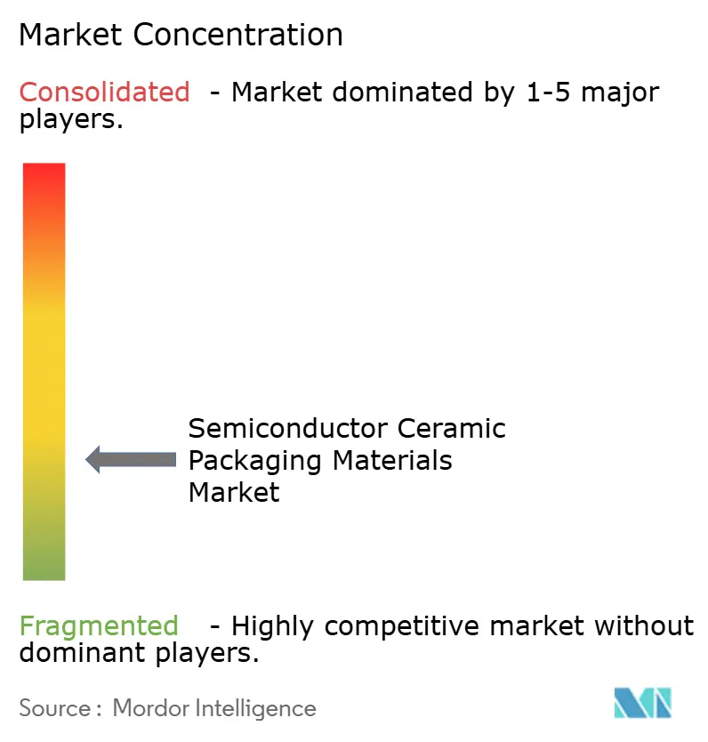
The semiconductor ceramic packaging materials market is highly fragmented, with the top five players including KYOCERA Corporation, NGK Corporation, Murata Manufacturing Co., Ltd., MARUWA CO., LTD., and CeramTec GmbH. KYOCERA Corporation completed the Nagasaki Isahaya Plant in September 2026 after a JPY 68 billion investment (approximately USD 453 million)[2]. The facility is designed to supply semiconductor packages for artificial intelligence data centers and electric vehicle applications. KYOCERA Corporation also commercialized a multilayer ceramic core substrate for xPU and switch application-specific integrated circuit packages in April 2026.
Rogers Corporation stated in its 2025 Form 10-K that its curamik advanced electronics solutions business serves fabricators and original equipment manufacturers in electric vehicles, wireless infrastructure, and energy applications. The company also disclosed restructuring at its Eschenbach facility to improve cost competitiveness. Ferrotec Corporation is expanding its ceramic manufacturing footprint in Japan and Malaysia. Its Malaysia facility responds to customers seeking production outside China.
NGK Corporation’s planned increase in HICERAM Carrier capacity reflects demand for chiplet integration and high-performance semiconductor applications. Resonac Holdings Corporation formed the JOINT3 consortium in September 2025 to develop panel-level organic interposer processes. AGC Inc. joined the initiative to work on glass carrier and interposer glass development. Chinese suppliers are expanding in commodity alumina packages, which places pricing pressure on standard packages while larger suppliers focus on high-value applications.
Semiconductor Ceramic Packaging Materials Industry Leaders
-
KYOCERA Corporation
-
NGK Corporation
-
Murata Manufacturing Co., Ltd.
-
MARUWA CO.,LTD.
-
CeramTec GmbH
- *Disclaimer: Major Players sorted in no particular order
Recent Industry Developments
- September 2026: Tokuyama Corporation announced plans to expand its aluminum nitride (AlN) powder production capacity by approximately 30% through a new manufacturing facility in Japan, with commercial operations scheduled for April 2028. The expansion supports the semiconductor ceramic packaging materials market by strengthening the supply of high-thermal-conductivity ceramic materials used in semiconductor manufacturing components and heat-dissipation applications.
- April 2026: Kyocera Corporation announced the commercialization of a multilayer ceramic core substrate for advanced semiconductor packages, including Artificial Intelligence (AI) processors and switch application-specific integrated circuits. The substrate is designed to reduce package warpage and enable high-density wiring, supporting the Semiconductor Ceramic Packaging Materials Market as AI infrastructure drives demand for advanced semiconductor packaging.
Global Semiconductor Ceramic Packaging Materials Market Report Scope
Semiconductor ceramic packaging materials are specialized ceramic materials used to encapsulate and protect semiconductor devices while providing electrical insulation, thermal management, and mechanical stability. Their properties support reliable operation in electronic packages exposed to demanding thermal, electrical, and environmental conditions.
The Semiconductor Ceramic Packaging Materials Market is segmented by material, packaging technology, end-use industry, and geography. By material, the market is segmented into alumina, aluminum nitride, silicon nitride, silicon carbide, beryllium oxide, and other materials. By packaging technology, the market is segmented into through-hole packages, surface mount packages - leaded, surface mount packages - leadless, advanced miniaturized packages, and other packaging technologies. By end-use industry, the market is segmented into consumer electronics, automotive, healthcare, IT and telecommunication, aerospace and defense, and other end-use industries. The report also covers the market size and forecasts for semiconductor ceramic packaging materials across 15 countries. For each segment, the market sizing and forecasts have been done on the basis of value (USD).
| Alumina |
| Aluminum Nitride |
| Silicon Nitride |
| Silicon Carbide |
| Beryllium Oxide |
| Other Materials |
| Through-Hole Packages |
| Surface Mount Packages - Leaded |
| Surface Mount Packages - Leadless |
| Advanced Miniaturized Packages |
| Other Packaging Technologies |
| Consumer Electronics |
| Automotive |
| Healthcare |
| IT and Telecommunication |
| Aerospace and Defense |
| Other End-Use Industries |
| Asia-Pacific | China |
| India | |
| Japan | |
| South Korea | |
| ASEAN Countries | |
| Rest of Asia-Pacific | |
| North America | United States |
| Canada | |
| Mexico | |
| Europe | Germany |
| United Kingdom | |
| France | |
| Italy | |
| NORDIC Countries | |
| Rest of Europe | |
| South America | Brazil |
| Argentina | |
| Rest of South America | |
| Middle East and Africa | Saudi Arabia |
| South Africa | |
| Rest of Middle East and Africa |
| By Material | Alumina | |
| Aluminum Nitride | ||
| Silicon Nitride | ||
| Silicon Carbide | ||
| Beryllium Oxide | ||
| Other Materials | ||
| By Packaging Technology | Through-Hole Packages | |
| Surface Mount Packages - Leaded | ||
| Surface Mount Packages - Leadless | ||
| Advanced Miniaturized Packages | ||
| Other Packaging Technologies | ||
| By End-Use Industry | Consumer Electronics | |
| Automotive | ||
| Healthcare | ||
| IT and Telecommunication | ||
| Aerospace and Defense | ||
| Other End-Use Industries | ||
| By Geography | Asia-Pacific | China |
| India | ||
| Japan | ||
| South Korea | ||
| ASEAN Countries | ||
| Rest of Asia-Pacific | ||
| North America | United States | |
| Canada | ||
| Mexico | ||
| Europe | Germany | |
| United Kingdom | ||
| France | ||
| Italy | ||
| NORDIC Countries | ||
| Rest of Europe | ||
| South America | Brazil | |
| Argentina | ||
| Rest of South America | ||
| Middle East and Africa | Saudi Arabia | |
| South Africa | ||
| Rest of Middle East and Africa | ||
Key Questions Answered in the Report
What is the size of the semiconductor ceramic packaging materials market?
The semiconductor ceramic packaging materials market size was valued at USD 2.01 billion in 2026 and is estimated to grow from USD 2.17 billion in 2027 to reach USD 3.26 billion by 2032, at a CAGR of 8.46% during the forecast period (2027-2032).
What materials held the largest share in 2026?
Alumina led with a 45.34% share in 2026.
Why are ceramic materials used in semiconductor packages?
Ceramics provide electrical insulation, hermeticity, and thermal performance that are important for high-power, high-frequency, and reliability-sensitive devices.
Which application is projected to grow fastest through 2032?
Automotive is projected to advance at a 9.67% CAGR through 2032, driven by power electronics in electric vehicles.