
Scientific CMOS Cameras For Industrial Research Market Size and Share
Market Overview
| Study Period | 2020 - 2031 |
|---|---|
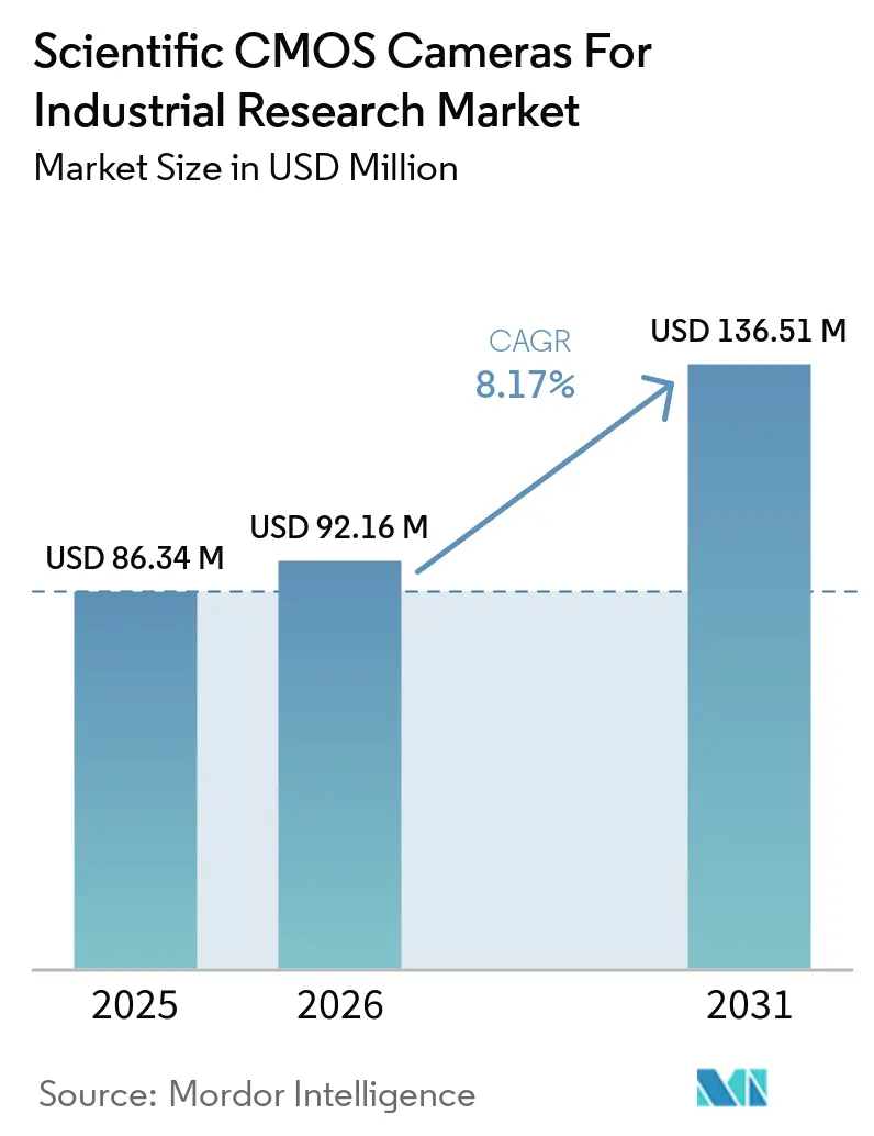
| Market Size (2026) | USD 92.16 Million |
| Market Size (2031) | USD 136.51 Million |
| Growth Rate (2026 - 2031) | 8.17 % |
| Fastest Growing Market | Asia-Pacific |
| Largest Market | Asia-Pacific |
| Market Concentration | Medium |
Major Players *Disclaimer: Major Players sorted in no particular order Image © Mordor Intelligence. Reuse requires attribution under CC BY 4.0. | |
Scientific CMOS Cameras For Industrial Research Market Analysis by Mordor Intelligence
The scientific CMOS cameras for industrial research market size is projected to expand from USD 86.34 million in 2025 and USD 92.16 million in 2026 to USD 136.51 million by 2031, registering a CAGR of 8.17% between 2026 to 2031. Laboratory-grade imaging is moving beyond specialist photonics laboratories into industrial research and development programs. Semiconductor analysis, battery imaging, and materials characterization are widening demand for high-performance platforms. These applications also favor back-illuminated, cooled, and multi-interface camera configurations, which carry higher selling prices than entry-level scientific imagers. Competition is becoming more demanding in the mid-priced range as Chinese suppliers expand from sensor supply into branded camera systems. Vendors can respond through cooling designs, application software, deep-ultraviolet sensor options, and closer relationships with original equipment manufacturers.
Key Report Takeaways
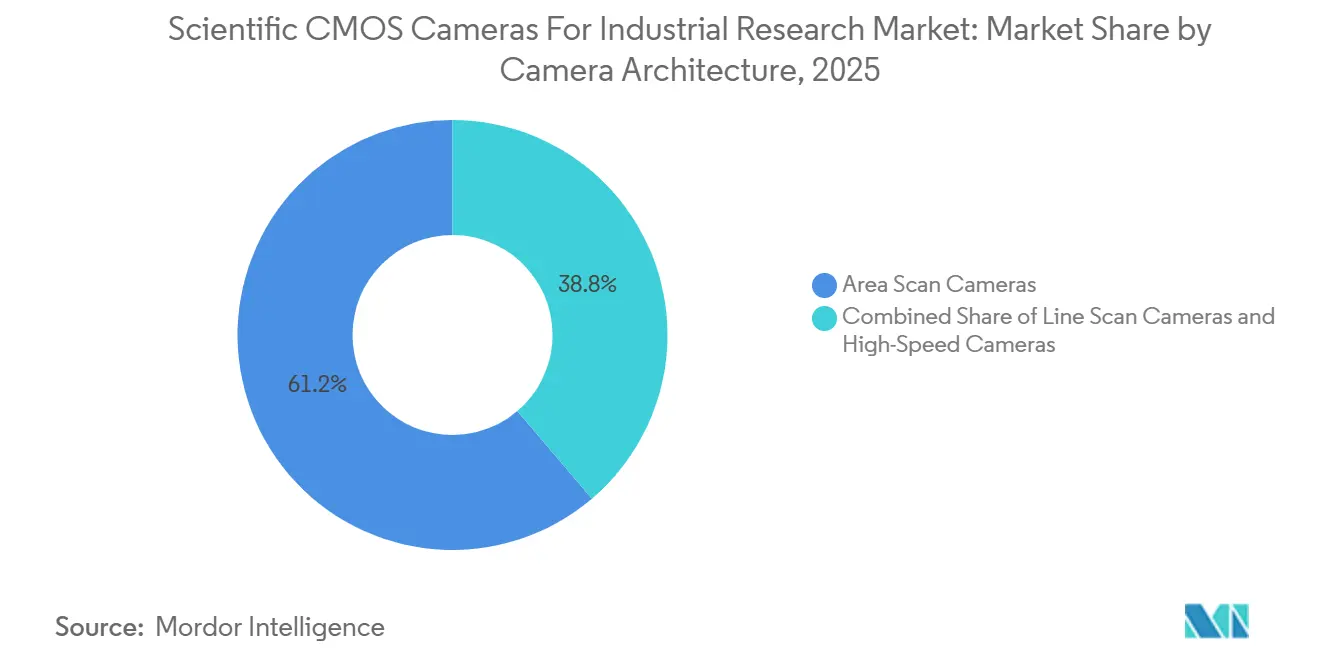
- By camera architecture, area scan cameras held 61.23% of the scientific CMOS cameras for industrial research market share in 2025, while high-speed cameras are projected to expand at a 9.39% CAGR through 2031.
- By imaging technology, scientific CMOS held 48.56% of the scientific CMOS cameras for industrial research market share in 2025, while back-illuminated scientific CMOS is projected to expand at an 8.91% CAGR through 2031.
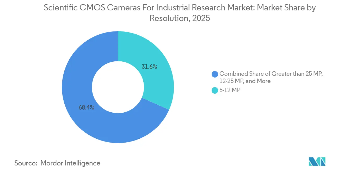
- By resolution, the 5-12 MP range accounted for 31.64% of the scientific CMOS cameras for industrial research market share in 2025 and is the fastest-expanding at an CAGR of 9.11% resolution class through 2031.
- By application, materials research and characterization held 22.97% of the scientific CMOS cameras for industrial research market share in 2025, while energy and battery research is projected to expand at a 9.09% CAGR through 2031.
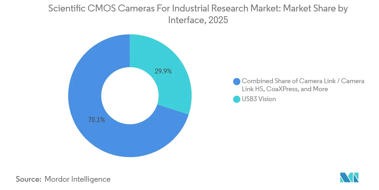
- By interface, USB3 Vision held 29.93% of the scientific CMOS cameras for industrial research market share in 2025, while CoaXPress is projected to expand at a 9.17% CAGR through 2031.
- By geography, Asia-Pacific held 34.38% of the scientific CMOS cameras for industrial research market share in 2025 and is projected to expand at an 8.89% CAGR through 2031.
Note: Market size and forecast figures in this report are generated using Mordor Intelligence’s proprietary estimation framework, updated with the latest available data and insights as of January 2026.
Market Trends and Insights
Drivers Impact Analysis of Scientific CMOS Cameras For Industrial Research Market*
| Driver | (~) % Impact on CAGR Forecast | Geographic Relevance | Impact Timeline |
|---|---|---|---|
| Mainstream Adoption of High-Speed Quantitative Imaging | +2.4% | Global, concentrated in North America, Japan, and Germany | Short term (≤ 2 years) |
| Back-Illuminated Sensor Efficiency in Photon-Starved Workflows | +1.9% | Global, strongest in Asia-Pacific and Europe | Medium term (2-4 years) |
| Growth of Live-Cell and High-Content Imaging | +1.5% | North America and Europe, with Asia-Pacific spillover | Medium term (2-4 years) |
| Expansion of Semiconductor and Photovoltaic Inspection | +1.1% | Asia-Pacific, especially South Korea, China, and Japan, with North America secondary | Short term (≤ 2 years) |
| OEM Integration of Compact Cooled Camera Platforms | +0.7% | Global, with early gains in Europe and North America | Medium term (2-4 years) |
| Demand for Synchronized Multimodal and Multidimensional Imaging | +0.5% | North America, Europe, and Japan | Long term (≥ 4 years) |
| Source: Mordor Intelligence | |||
Mainstream Adoption of High-Speed Quantitative Imaging
High-speed quantitative imaging is now used across materials testing, aerodynamics research, and battery development. This change extends the scientific CMOS cameras for industrial research market beyond specialist particle physics and plasma laboratories. A 2025 study reported an sCMOS-based light-sheet microscopy system that captured more than 1,000 volumes per second.[1] The result demonstrated millisecond-scale temporal resolution for a wider group of research workflows. Published protocols make advanced imaging methods easier to specify in equipment purchases. That shift can turn camera procurement from a discretionary decision into a required part of an experimental system.
A February 2026 paper described a global-shutter CMOS imager that sustained 1,141 frames per second at UHD resolution within a 5.5 W power envelope. The reported performance shows that frame rate and compact form factor can now be combined in one design. Industrial original equipment manufacturers can use that combination where space and power limits previously restricted camera selection. The scientific CMOS cameras for industrial research market therefore benefits from demand in adjacent uses that previously relied on lower-cost CCD or EMCCD systems. Faster acquisition also helps researchers observe short events in material changes and fluid behavior. Suppliers that pair camera hardware with stable acquisition tools are better placed to support these uses.
Back-Illuminated Sensor Efficiency in Photon-Starved Workflows
Back-illuminated sCMOS sensors can achieve peak quantum efficiency above 95% in the visible spectrum. This is a 15-20 percentage-point advantage over front-illuminated variants in the supplied analysis. Higher sensitivity supports shorter exposure times and stronger signal quality in low-light workflows. These workflows include single-molecule fluorescence and thin-film defect luminescence analysis. The scientific CMOS cameras for industrial research market benefits when these applications require more capable imaging systems. The performance difference also makes a back-illuminated design relevant for users replacing older detector technologies.
Hamamatsu Photonics launched the ORCA-Halo in May 2025 with 86% peak quantum efficiency, 9 MP resolution, and forced-air or water-cooling options.[2] The product targeted original equipment manufacturers and academic users needing high-sensitivity routine inspection. Back-illuminated cameras are also replacing EMCCD detectors in semiconductor emission microscopy. This expands the replacement opportunity beyond the core back-illuminated camera base. In July 2026, Hamamatsu began taking orders for the Solid Cold Emmi-X, which uses linear solid-state cooling rather than liquid nitrogen for continuous semiconductor laboratory operation. The system was priced at JPY 130 million pre-tax, USD 0.88 million per system, and shows the move toward maintenance-free, high-reliability platforms.
Growth of Live-Cell and High-Content Imaging
Live-cell and high-content imaging require low read noise, fast acquisition, broad field coverage, and reduced phototoxicity. Scientific CMOS platforms address these needs within a single camera architecture. A 2025 PhotoniX study used spinning-disk light-sheet microscopy with deep-learning restoration to image full mouse brains at single-neuron resolution.[3] The work used sCMOS detectors as the primary acquisition component. It shows why microscope manufacturers increasingly specify sCMOS sensors during platform design rather than treat cameras as interchangeable accessories. This practice strengthens long-term supply relationships in the scientific CMOS cameras for industrial research market.
High-content screening evaluates thousands of drug candidates in parallel. The method is moving from fixed-endpoint assays toward live-cell protocols that collect dynamic data. A 2025 Nature Communications study described real-time, high-throughput super-resolution microscopy using panoramic integration. Such workflows can require 50-100 frames per second for extended periods. This requirement places cameras within pharmaceutical automation infrastructure rather than at the edge of a laboratory workflow. Vendors that support dependable sustained acquisition can benefit as life-science systems become more automated.
Expansion of Semiconductor and Photovoltaic Inspection
Semiconductor production at nodes below 3 nm requires inspection systems that can work at deep-ultraviolet wavelengths. Conventional silicon CMOS sensors lose efficiency at 266 nm and 355 nm without specialized back-thinning and anti-reflection coatings. This requirement creates demand for sCMOS sensors designed for wafer defect detection. The scientific CMOS cameras for industrial research market gains from the upgrade cycles tied to new process nodes. These cycles affect both front-end inspection and back-end failure analysis. Camera vendors need sensor performance, interface bandwidth, and reliable system integration to address this requirement.
Tucsen Photonics launched the Gemini 8KTDI in March 2025 with a 1 MHz line rate at 8K resolution and a 100G CoaXPress-over-Fiber interface. The camera reported 63.9% quantum efficiency at 266 nm for deep-ultraviolet inspection. Gpixel announced its GLT5009BSI-DUV variant in August 2024 with quantum efficiency above 50% at 266 nm and above 30% at 200 nm. Heterojunction and perovskite photovoltaic manufacturing also needs electroluminescence and photoluminescence imaging at production scale. This creates demand for high-throughput area scan systems at price points below those of semiconductor-grade inspection cameras.
Restraints Impact Analysis of Scientific CMOS Cameras For Industrial Research Market*
| Restraint | (~) % Impact on CAGR Forecast | Geographic Relevance | Impact Timeline |
|---|---|---|---|
| High Acquisition Cost and Specialized Integration Requirements | -1.4% | Global, most acute in South America and the Middle East and Africa | Short term (≤ 2 years) |
| Limited Availability of Scientific Imaging Specialists | -0.8% | Global, most pronounced in emerging markets | Medium term (2-4 years) |
| Sensor and Semiconductor Supply-Chain Concentration | -0.6% | Global, with high risk in regions dependent on Asia-Pacific fabrication facilities | Medium term (2-4 years) |
| Data-Throughput, Storage, and Workflow Bottlenecks | -0.4% | Global, concentrated at high-resolution and high-frame-rate installations | Long term (≥ 4 years) |
| Source: Mordor Intelligence | |||
High Acquisition Cost and Specialized Integration Requirements
Premium cooled sCMOS systems routinely cost USD 30,000-80,000 per unit. Frame grabbers, high-bandwidth cables, and custom software can double the total purchase cost for an industrial research deployment. This cost is especially difficult for mid-sized research and development centers and contract research organizations. These users may not have dedicated budgets for scientific imaging infrastructure. Separate interface standards also add lifecycle costs because Camera Link HS, CoaXPress 2.0, and USB3 Vision require different frame grabbers and software stacks. The resulting complexity limits volume adoption in price-sensitive parts of the scientific CMOS cameras for industrial research market.
Excelitas Technologies launched the pco.pixelfly 10 bi CLHS in November 2025. The air-cooled 10.4 MP back-illuminated sCMOS camera was intended for original equipment manufacturers and laboratory users at a lower price point. Its design removes liquid-cooling complexity while retaining low-noise performance. This product response shows that suppliers recognize the cost barrier. It does not remove the need for compatible hardware, software, and specialized installation work. Standardized and lower-cost integration routes remain necessary for wider adoption.
Limited Availability of Scientific Imaging Specialists
Cooled sCMOS systems require knowledge of sensor physics, optical alignment, acquisition software, and data-pipeline management. These skills are concentrated among imaging scientists at large universities and national laboratories. Limited specialist availability can delay deployments and leave advanced camera capabilities underused. It can also increase the support cost faced by industrial users. The movement from CCD to sCMOS cameras introduced rolling-shutter artifacts, spatially variable noise, and new calibration requirements. This transition requires retraining as experienced CCD-era scientists retire.
Post-sale technical support is therefore an important competitive factor in the scientific CMOS cameras for industrial research market. Suppliers with application engineering teams can provide remote calibration and workflow integration services. These capabilities can support repeat purchases more effectively than a hardware-only offering. Specialist availability is particularly limited in parts of South America, Southeast Asia, and the Middle East and Africa. Procurement can remain constrained in these locations even when budgets are available. Training and remote support services can help suppliers address this constraint without changing the camera hardware itself.
*Our forecasts treat driver/restraint impacts as directional, not additive. The impact forecasts reflect baseline growth, mix effects, and variable interactions.
Scientific CMOS Cameras For Industrial Research Market Segment Analysis
By Camera Architecture:
Area Scan Platforms Anchor Volume While High-Speed Variants AccelerateArea scan cameras held 61.23% of the scientific CMOS cameras for industrial research market share in 2025. Their position reflects use in wide-field fluorescence microscopy, materials characterization, and semiconductor photoluminescence inspection. These applications need full-frame sensitivity and even illumination. They do not always need line-by-line acquisition speed. Area scan geometry is deeply established in scientific instruments, including life-science confocal systems and industrial metrology tools. This installed design base makes replacement by other formats difficult after an original equipment manufacturer has selected a sensor configuration. The scientific CMOS cameras for industrial research industry retains a broad volume base through these established uses.
Line scan cameras serve continuous inspection of printed electronics, solar cell ribbon, and battery electrode coating lines. They offer speed and spatial coverage that area sensors cannot provide in moving-web processes. High-speed cameras are projected to expand at a 9.39% CAGR through 2031. Demand comes from laser-material interaction studies, transient combustion analysis, and aerodynamics research. A 2025 Optica study reported a 25-camera multifocus array that captured three-dimensional volumes at more than 100 volumes per second. This type of system establishes a performance requirement for high-speed sCMOS cameras in dynamic experiments. The movement from dedicated ultrafast systems toward general-purpose scientific CMOS platforms supports this architecture's faster expansion.

By Imaging Technology:
Scientific CMOS Leads, Back-Illuminated Sensors Set the Benchmark for Low-Noise PerformanceScientific CMOS accounted for 48.56% of the scientific CMOS cameras for industrial research market share by imaging technology in 2025. It is widely used in standard fluorescence microscopy, quantitative phase imaging, and general industrial research and development. More than a decade of original equipment manufacturer integration supports its installed base. That installed base contributes to repeat-purchase cycles and ongoing volume demand. The technology offers a familiar platform for users that need a balance of sensitivity, speed, and field coverage. This position makes scientific CMOS the core imaging approach within the scientific CMOS cameras for industrial research industry.
Back-illuminated sCMOS is projected to expand at an 8.91% CAGR through 2031. It benefits from the move away from EMCCD and high-end CCD detectors in photon-starved imaging work. Oxford Instruments' Andor division launched the CB2 24B in January 2025 with a 24.5 MP back-illuminated global-shutter sensor. The design supports wide field coverage and motion-blur-free acquisition in high-content screening and manufacturing inspection. Global-shutter CMOS remains important where wafer and panel inspection systems must synchronize each pixel with pulsed laser illumination. Other imaging technologies, including hyperspectral CMOS derivatives, remain early-stage but relevant. Fraunhofer IPMS described a compact artificial intelligence-enabled hyperspectral camera using a standard two-dimensional CMOS sensor in 2026.
By Resolution:
Mid-Range Sensors Dominate Across ApplicationsThe 5-12 MP category accounted for 31.64% of the scientific CMOS cameras for industrial research market size in 2025. It is also the fastest-expanding resolution class through 2031 at an CAGR of 9.11%. This dual position reflects the fit between this resolution range and common sCMOS sensor formats. The range supports large-field fluorescence tiling and semiconductor photoluminescence mapping. It also keeps data rates manageable for USB3 Vision and GigE interfaces. This practical balance matters in laboratories that continue to use legacy computing infrastructure.
The 12-25 MP tier is gaining use as high-content workflows require greater field coverage. Cameras such as the Andor CB2 24B can reduce the need for mosaic acquisition and subsequent image stitching. Cameras below 2 MP continue in specialized spectroscopy and fiber-coupled applications. In these applications, the detector is secondary to the spectrometer. Resolutions above 25 MP remain limited outside space-qualified and aerial survey uses. Artificial intelligence-guided inspection tools are beginning to favor the 5-12 MP and 12-25 MP ranges. These tools combine high-resolution frames with on-edge inference and can gain more from pixel count than frame rate for static or slowly moving samples.
By Application:
Materials Characterization Leads While Energy Research Drives the Next CycleMaterials research and characterization accounted for 22.97% of the scientific CMOS cameras for industrial research market size in 2025. Academic consortia, national laboratories, and materials suppliers use these systems to assess thin-film quality, grain-boundary behavior, and surface defects. This work requires repeatable imaging of physical changes across samples. Semiconductor and electronics research and development is the next-largest application area. Deep-ultraviolet inspection needs can raise unit pricing in this segment. Suppliers with specialized anti-reflection coatings have a clear technical position in these systems.
Energy and battery research is projected to expand at a 9.09% CAGR through 2031. Operando imaging is becoming a standard characterization step in next-generation battery-cell development. A 2025 Journal of The Electrochemical Society article described sCMOS sensors as primary detectors for real-time tracking of dendrite nucleation and state-of-charge changes during cycling. Fraunhofer EMI reported an X-ray imaging system in August 2026 that captured 1,000 frames per second for in-operando battery-cell analysis. Aerospace and automotive research and development remains a stable application area shaped by defense and electric-vehicle budgets. Semiconductor equipment certification under SEMI F47 and component reliability expectations in aerospace inspection favor suppliers that can provide traceable calibration records.
By Interface:
USB3 Vision Holds the Installed Base While CoaXPress Gains Industrial MomentumUSB3 Vision held 29.93% of the scientific CMOS cameras for industrial research market share by interface in 2025. The standard is common in laboratory computing environments. Plug-and-play support with standard Windows and Linux software development kits lowers deployment time and information technology complexity. This makes USB3 Vision a practical choice for general research imaging. Its installed base gives users a familiar integration route. This advantage remains important where laboratories need capable systems without extensive infrastructure changes.
CoaXPress is projected to expand at a 9.17% CAGR through 2031. Demand is linked to the bandwidth needs of 8K and 16K time-delay-integration sCMOS cameras in semiconductor inspection and advanced manufacturing. CoaXPress 2.0 supports 12.5 Gbps per link through standard coaxial cable and can provide power delivery. This arrangement supports multi-camera inspection cells without dedicated power cables. GigE and 10GigE Vision remain relevant in factories that use shared Ethernet infrastructure to reduce cabling cost. Camera Link and Camera Link HS continue to support established life-science microscopy integrations. The anticipated CoaXPress v3.0 specification could maintain interface demand as sensor resolution rises.
Geography Analysis
APAC Scientific CMOS Cameras for Industrial Research Market
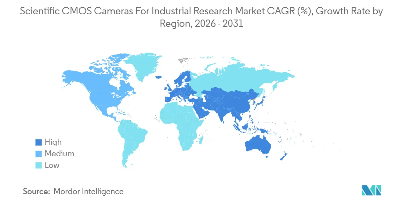
Asia-Pacific held 34.38% of the scientific CMOS cameras for industrial research market share in 2025 and is projected to expand at an 8.89% CAGR through 2031. China, Japan, South Korea, and Taiwan account for much of global wafer fabrication capacity. Each process-node transition from 3 nm to 2 nm and below requires updates in front-end defect detection and back-end failure analysis. These upgrades support recurring camera demand across semiconductor tool chains. Hamamatsu reported industrial-segment revenue of JPY 39.2 billion, USD 261 million, in the first half of fiscal year 2026. This was a 4.5% increase from the same period of fiscal year 2025 and reflected demand from semiconductor and advanced manufacturing customers.
Europe, North America and APAC Scientific CMOS Cameras for Industrial Research Market
India, South Korea's ASEAN supply-chain satellites, and Australia represent the next tier of regional demand. India and Australia are developing quantum, photonics, and related research capabilities. These locations can take a larger share of compact air-cooled sCMOS platforms in the latter part of the forecast period. North America and Europe remain established centers for scientific research imaging. North American demand is supported by research universities, National Institutes of Health-funded life-science programs, and semiconductor-equipment original equipment manufacturers. United States Department of Energy battery programs also create demand for operando imaging systems. The scientific CMOS cameras for industrial research market size in these regions is supported by applications that require high-value camera configurations.
EMEA and South America Scientific CMOS Cameras for Industrial Research Market
In Europe, Germany, the United Kingdom, and France host major photonics instrument manufacturers and public research infrastructure. Southern and Eastern Europe are emerging areas as European Union Horizon funding increases equipment spending. CEA and ESRF reported the first operando synchrotron imaging study of complete all-solid-state microbatteries in August 2026. The European Union Chips Act and related public commitments support domestic semiconductor-equipment development. South America, the Middle East, and Africa hold a smaller combined share but offer distinct sources of demand. Brazil is the main South American center, although imported equipment raises price sensitivity. Saudi Arabia and the United Arab Emirates are expanding university and semiconductor-adjacent facilities, while Africa remains concentrated in South African mining and materials research. Specialist shortages are strongest in these regions, which makes training and remote-support packages central to vendor access.
Competitive Landscape
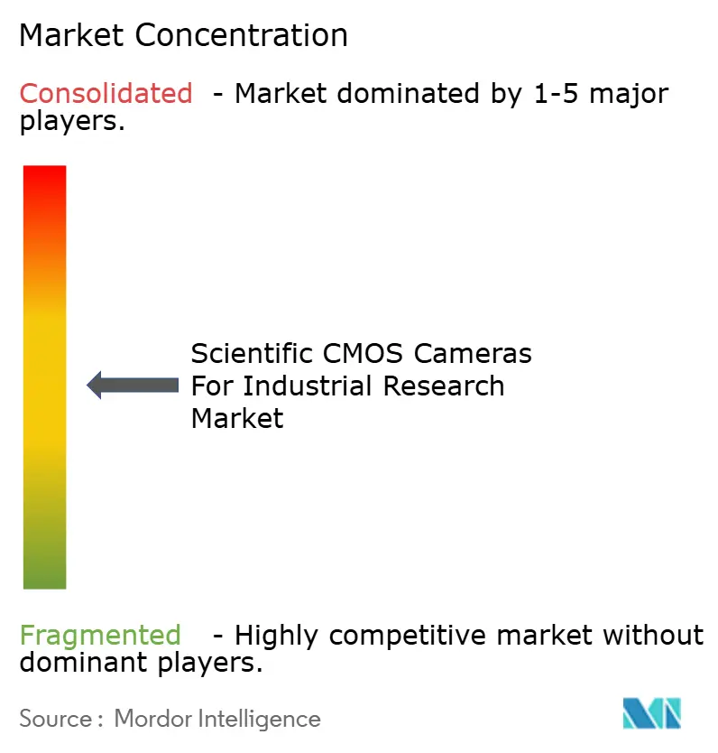
The scientific CMOS cameras for industrial research market has moderate concentration in the premium tier. Hamamatsu Photonics, Oxford Instruments through Andor, and Teledyne Technologies are leading suppliers in this tier. Proprietary sensor fabrication, original equipment manufacturer relationships, and application-specific platforms support their position. The sub-USD 10,000 range is more fragmented. XIMEA, PCO, IMPERX, Raptor Photonics, and Atik serve narrower applications where cooling design, interface compatibility, and existing installation bases determine the supplier choice. This difference between premium concentration and lower-priced fragmentation shapes the competitive position of the scientific CMOS cameras for industrial research industry.
Tucsen Photonics and Gpixel are moving from sensor intellectual property and volume supply into branded camera platforms. They compete in semiconductor inspection through price, lead time, and domestic supply-chain reliability. Gpixel announced the GLT5009BSI-DUV sensor with specialized deep-ultraviolet capability in August 2024. Its United States and international patent filings cover deep-ultraviolet anti-reflection architectures. This move shows an approach based on protected design capability rather than hardware manufacturing alone. Existing suppliers need to maintain differentiation through sensor performance and system support.
Leading companies are upgrading from front-illuminated designs to back-illuminated architectures. They are also reducing camera size for original equipment manufacturer integration and adding CoaXPress 2.0 alongside USB3 and Camera Link options. Hamamatsu's ORCA-Quest family is embedded in quantum-optics platforms, where replacement cycles can extend for 5-10 years. That installation base makes original equipment manufacturer channels a durable advantage. SinceVision launched the Solis BSI Series in November 2025 with claimed 0.5 e⁻ read noise and vacuum-sealed cooling. The product shows that newer suppliers can approach established back-illuminated platform specifications, while energy-storage research remains an opening for mid-tier vendors to build reference accounts.
Scientific CMOS Cameras For Industrial Research Industry Leaders
-
Hamamatsu Photonics K.K.
-
Oxford Instruments plc
-
Teledyne Technologies Incorporated
-
Excelitas Technologies Corp.
-
Thorlabs, Inc.
- *Disclaimer: Major Players sorted in no particular order
Scientific CMOS Cameras For Industrial Research Market Companies Covered in this Report
- Hamamatsu Photonics K.K.
- Oxford Instruments plc
- Teledyne Technologies Incorporated
- Excelitas Technologies Corp.
- Thorlabs, Inc.
- Gpixel NV
- XIMEA GmbH
- Diffraction Limited
- HORIBA, Ltd.
- Photonic Science and Engineering Limited
- Tucsen Photonics Co., Ltd.
- Raptor Photonics Limited
- IMPERX, Inc.
- Vieworks Co., Ltd.
- QImaging
- Atik Cameras Limited
- Spectral Instruments, Inc.
- Meiji Techno Co., Ltd.
- PCO AG
- SinceVision, Inc.
Recent Industry Developments in Scientific CMOS Cameras For Industrial Research Market
- August 2026: Fraunhofer Institute for High-Speed Dynamics (EMI) published results for an operando X-ray imaging system capable of capturing 1,000 frames per second inside live battery cells, developed in partnership with PowerCo (Volkswagen). The system integrates high-performance sCMOS detectors and reveals real-time gas formation, material displacement, and thermal dynamics, with a full commercial installation at PowerCo's Salzgitter site planned for 2028.
- August 2026: A consortium of CEA-Irig, CEA-Leti, and the European Synchrotron Radiation Facility (ESRF) reported the first operando X-ray monitoring of a complete all-solid-state microbattery, achieving micrometer-scale spatial resolution. The breakthrough establishes a direct demand anchor for ultra-high-frame-rate sCMOS cameras in synchrotron-adjacent research infrastructure.
- July 2026: Hamamatsu Photonics began taking orders for the Solid Cold Emmi-X camera, a liquid-nitrogen-free BSI emission analysis system priced at JPY 130 million pre-tax, USD 0.88 million per unit, targeting semiconductor failure analysis of advanced logic and high-density memory devices. Sales targets are 10 systems in year 1 and 15 in year 5, with a demonstration at IPFA2026 in Singapore.
- July 2026: Hamamatsu Photonics Europe launched active promotion of Fairchild Imaging CMOS sensor technologies across European customers following Hamamatsu's 2024 acquisition of Fairchild Imaging, expanding the group's addressable market to include X-ray, space-qualified, and medical-grade CMOS imaging with noise performance as low as 0.25 e⁻ RMS.
Global Scientific CMOS Cameras For Industrial Research Market Report Scope
The Scientific CMOS (sCMOS) Cameras for Industrial Research Market comprises high-performance imaging systems based on scientific complementary metal-oxide-semiconductor (sCMOS) sensor technology, designed to deliver high sensitivity, low noise, fast frame rates, wide dynamic range, and superior image resolution for advanced industrial research applications.
The Scientific CMOS Cameras for Industrial Research Market Report is Segmented by Camera Architecture (Area Scan Cameras, Line Scan Cameras, and High-Speed Cameras), Imaging Technology (Scientific CMOS (sCMOS), Back-Illuminated sCMOS (BSI), Global-Shutter CMOS, and Other Imaging Technologies), Resolution (Less than 2 MP, 2–5 MP, 5–12 MP, 12–25 MP, and Greater than 25 MP), Application (Materials Research and Characterization, Semiconductor and Electronics R&D, Photonics and Optics Research, Advanced Manufacturing Research, Energy and Battery Research, Aerospace and Automotive R&D, and Other Applications), Interface (USB3 Vision, GigE/10GigE Vision, Camera Link/Camera Link HS, CoaXPress, and Other Interfaces), and Geography (North America, South America, Europe, Asia-Pacific, and Middle East and Africa). The Market Forecasts are Provided in Terms of Value (USD).
Segmentation Overview
| Area Scan Cameras |
| Line Scan Cameras |
| High-Speed Cameras |
| Scientific CMOS (sCMOS) |
| Back-Illuminated sCMOS (BSI) |
| Global-Shutter CMOS |
| Other Imaging Technologies |
| Less than 2 MP |
| 2-5 MP |
| 5-12 MP |
| 12-25 MP |
| Greater than 25 MP |
| Materials Research and Characterization |
| Semiconductor and Electronics R&D |
| Photonics and Optics Research |
| Advanced Manufacturing Research |
| Energy and Battery Research |
| Aerospace and Automotive R&D |
| Other Applications |
| USB3 Vision |
| GigE / 10GigE Vision |
| Camera Link / Camera Link HS |
| CoaXPress |
| Other Interfaces |
| North America | United States | |
| Canada | ||
| Mexico | ||
| South America | Brazil | |
| Argentina | ||
| Rest of South America | ||
| Europe | Germany | |
| United Kingdom | ||
| France | ||
| Italy | ||
| Spain | ||
| Rest of Europe | ||
| Asia-Pacific | China | |
| Japan | ||
| India | ||
| South Korea | ||
| ASEAN | ||
| Rest of Asia-Pacific | ||
| Middle East and Africa | Middle East | Saudi Arabia |
| United Arab Emirates | ||
| Rest of the Middle East | ||
| Africa | South Africa | |
| Rest of Africa | ||
| By Camera Architecture | Area Scan Cameras | ||
| Line Scan Cameras | |||
| High-Speed Cameras | |||
| By Imaging Technology | Scientific CMOS (sCMOS) | ||
| Back-Illuminated sCMOS (BSI) | |||
| Global-Shutter CMOS | |||
| Other Imaging Technologies | |||
| By Resolution | Less than 2 MP | ||
| 2-5 MP | |||
| 5-12 MP | |||
| 12-25 MP | |||
| Greater than 25 MP | |||
| By Application | Materials Research and Characterization | ||
| Semiconductor and Electronics R&D | |||
| Photonics and Optics Research | |||
| Advanced Manufacturing Research | |||
| Energy and Battery Research | |||
| Aerospace and Automotive R&D | |||
| Other Applications | |||
| By Interface | USB3 Vision | ||
| GigE / 10GigE Vision | |||
| Camera Link / Camera Link HS | |||
| CoaXPress | |||
| Other Interfaces | |||
| By Geography | North America | United States | |
| Canada | |||
| Mexico | |||
| South America | Brazil | ||
| Argentina | |||
| Rest of South America | |||
| Europe | Germany | ||
| United Kingdom | |||
| France | |||
| Italy | |||
| Spain | |||
| Rest of Europe | |||
| Asia-Pacific | China | ||
| Japan | |||
| India | |||
| South Korea | |||
| ASEAN | |||
| Rest of Asia-Pacific | |||
| Middle East and Africa | Middle East | Saudi Arabia | |
| United Arab Emirates | |||
| Rest of the Middle East | |||
| Africa | South Africa | ||
| Rest of Africa | |||
Key Questions Answered in the Report
What is the 2026 size of the scientific CMOS cameras for industrial research market?
The scientific CMOS cameras for industrial research market was estimated at USD 92.16 million in 2026 and is projected to reach USD 136.51 million by 2031.
What is driving demand for scientific CMOS cameras in industrial research?
Demand is supported by high-speed quantitative imaging, low-light back-illuminated sensors, live-cell imaging, and semiconductor and photovoltaic inspection.
Which camera architecture holds the largest share?
Area scan cameras held 61.23% market share in 2025 because they are widely used in wide-field microscopy, materials research, and semiconductor inspection.
Which application is projected to expand fastest through 2031?
Energy and battery research is projected to expand at a 9.09% CAGR through 2031 as operando electrochemical imaging becomes more common.
Why is CoaXPress gaining use in scientific imaging systems?
CoaXPress supports the bandwidth requirements of 8K and 16K time-delay-integration cameras used in semiconductor inspection and manufacturing quality control.
Which region leads demand for scientific CMOS cameras for industrial research?
Asia-Pacific held 34.38% market share in 2025 and is projected to expand at an 8.89% CAGR through 2031, supported by semiconductor capacity expansion and research investment.