
Quartz and Glass Wafer Carrier Market Size and Share
Market Overview
| Study Period | 2021 - 2032 |
|---|---|
| Market Size (2027) | USD 334.59 Million |
| Market Size (2032) | USD 471.19 Million |
| Growth Rate (2027 - 2032) | 7.09 % |
| Fastest Growing Market | Asia-Pacific |
| Largest Market | North America |
| Market Concentration | Medium |
Major Players *Disclaimer: Major Players sorted in no particular order Image © Mordor Intelligence. Reuse requires attribution under CC BY 4.0. | |
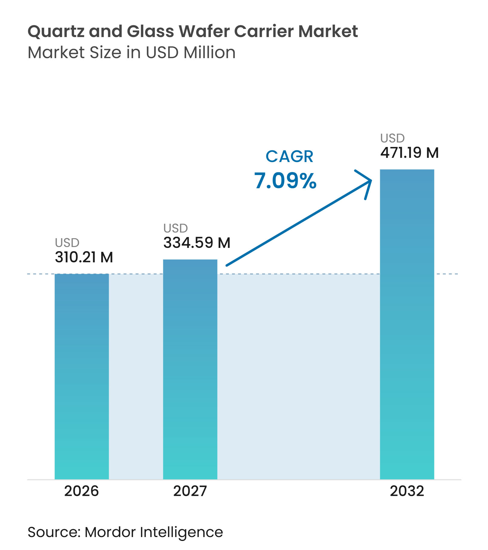
Quartz and Glass Wafer Carrier Market Analysis by Mordor Intelligence
The Quartz and Glass Wafer Carrier Market size is projected to expand from USD 310.21 million in 2026 and USD 332.20 million in 2027 to USD 471.19 million by 2032, registering a 7.09% CAGR over 2027-2032. Demand is tied to components that support wafer handling in thermal diffusion, chemical vapor deposition, and advanced packaging operations, where repeatability protects process quality and equipment uptime. Expansion of 300 mm front-end production increases demand for replacements of high-purity boats, tubes, and carriers that must perform reliably through repeated thermal cycles. Packaging programs that use fan-out and chiplet designs require flat, thermally stable glass carriers for thinning, bonding, deposition, and annealing. Power device production also creates demand for carriers that meet the tighter tolerances associated with silicon carbide and gallium nitride processing. Suppliers are therefore competing on material purity, dimensional consistency, traceability, and the ability to qualify products with semiconductor customers, rather than on price alone.
Key Report Takeaways
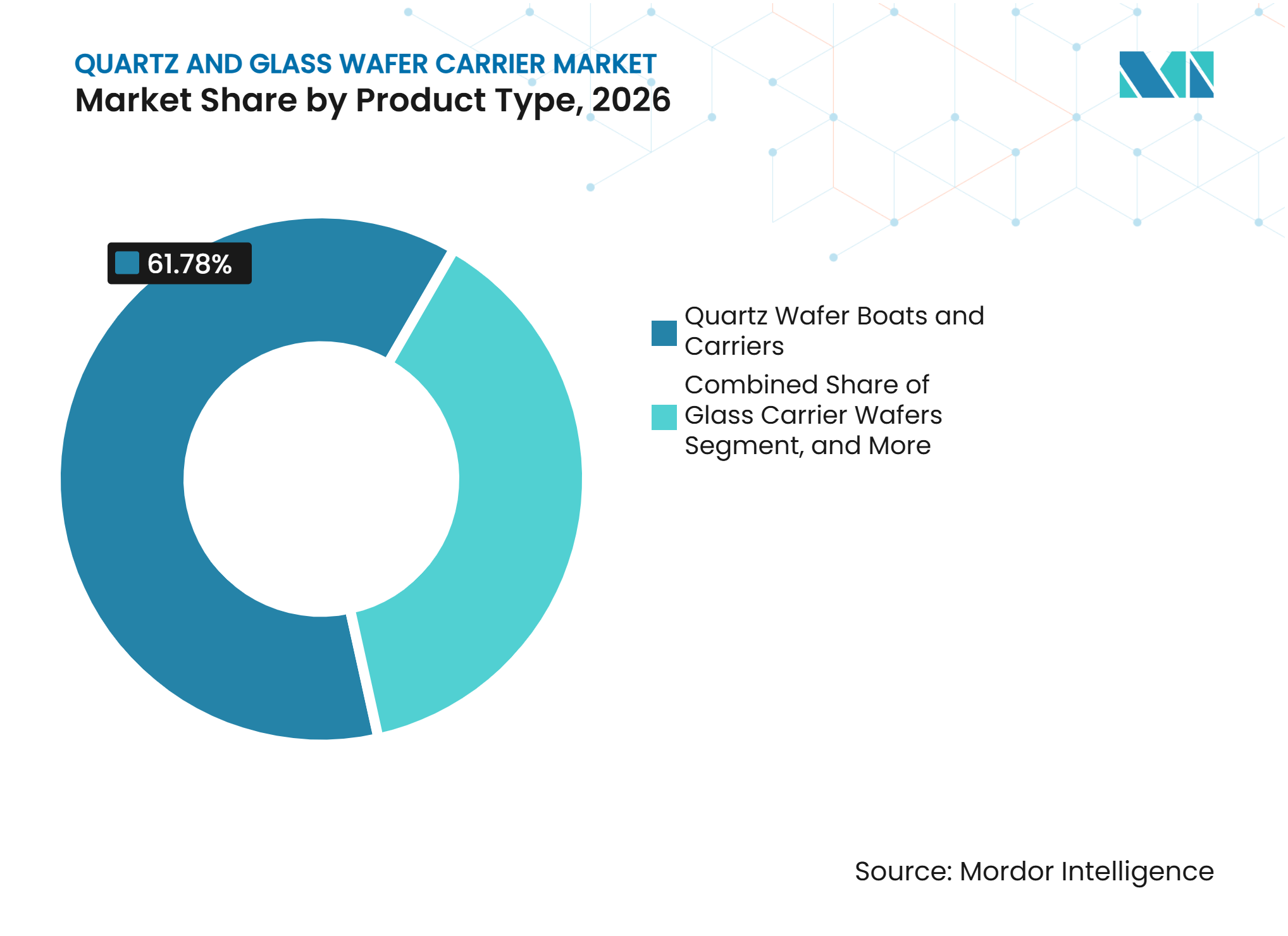
- By product type, quartz wafer boats and carriers held 61.78% of the quartz and glass wafer carrier market share in 2026, while glass carrier wafers are projected to expand at an 8.26% CAGR through 2032.
- By process application, LPCVD accounted for 26.59% of the Quartz and Glass Wafer Carrier Market size in 2026, while compound semiconductor processing is projected to record the highest CAGR at 9.92% through 2032.
- By wafer and carrier size, 300 mm carriers held 38.92% of the quartz and glass wafer carrier market revenue share in 2026, while panel-format carriers are expected to expand at an 8.39% CAGR through 2032.
- By end-use customer, IDMs accounted for 36.47% share in 2026, while compound semiconductor fabs are projected to advance at a 10.59% CAGR through 2032.
- By geography, Asia-Pacific held 67.98% of the quartz and glass wafer carrier market share in 2026 and is projected to register an 11.91% CAGR through 2032.
Note: Market numbers in this report are based on Mordor Intelligence's proprietary estimation framework, which combines nine months of actuals with Q4 projections for base year 2026.
Market Trends and Insights
Drivers Impact Analysis of Quartz and Glass Wafer Carrier Market*
| Driver | (~) % Impact on CAGR Forecast | Geographic Relevance | Impact Timeline |
|---|---|---|---|
| Growth in AI Accelerators and Advanced Memory Packaging | +2.1% | Global, concentrated in Taiwan and South Korea | Short term (≤ 2 years) |
| Expansion of Fan-Out Wafer-Level and Panel-Level Packaging | +1.8% | Asia-Pacific core, with spillover to North America | Short term (≤ 2 years) |
| Expansion of Compound Semiconductor Manufacturing | +1.5% | Global, led by China, United States, Europe, and East Asia | Medium term (2-4 years) |
| Increasing Adoption of Chiplet and Heterogeneous Integration | +1.2% | Global, primarily Asia-Pacific and North America | Medium term (2-4 years) |
| Sustained Demand for Quartzware in Legacy-Node Fabs | +0.8% | Asia-Pacific and North America | Long term (≥ 4 years) |
| Shift Toward High-Precision Synthetic Quartz Carriers | +0.6% | Japan, Germany, and United States | Long term (≥ 4 years) |
| Source: Mordor Intelligence | |||
Growth in AI Accelerators and Advanced Memory Packaging
AI accelerator production increases the number of thermal and deposition steps used in advanced semiconductor packaging, as component suppliers operate under tightly specified customer approval requirements. These steps require quartz components that can withstand repeated high-temperature processing without introducing contamination and protect sensitive wafer surfaces and deposited layers, where reliable operation matters throughout high-temperature and advanced packaging steps. Advanced memory packages also increase the importance of stable carrier surfaces during deposition, annealing, and wafer handling, particularly when several dies are integrated within a package, while meeting application-specific requirements that can differ by customer and toolset. The Quartz and Glass Wafer Carrier Market benefits because the value of qualified consumables rises with process complexity rather than only with wafer volumes. Customers in Taiwan and South Korea are particularly relevant because advanced foundry and memory operations are concentrated there, while maintaining the validation standards expected in semiconductor manufacturing. SCHOTT has positioned glass carrier products for advanced packaging, wafer thinning, and fan-out applications, reflecting the industry's response to these process requirements, while preserving the dimensional stability required in sensitive applications.
Expansion of Fan-Out Wafer-Level and Panel-Level Packaging
Fan-out packaging broadens the use of glass carriers because thin wafers require mechanical support during temporary bonding and processing. Panel-level production adds larger formats that need controlled flatness and closely managed thermal expansion across the full processing surface. This requirement creates a separate qualification path from conventional quartz boats used in furnace operations, because materials and mechanical behavior differ. The Quartz and Glass Wafer Carrier Market gains new opportunities as packaging firms adopt rectangular-panel processes alongside established round-wafer production. ASE has described 300 mm panel-level fan-out work that uses chip-last processing, showing how packaging development can alter carrier requirements.[1] Suppliers that can provide repeatable glass quality and application support are better placed to serve these programs.
Expansion of Compound Semiconductor Manufacturing
Silicon carbide and gallium nitride fabrication increases the need for carriers that meet specialized reactor and thermal-processing requirements, as component suppliers work within tightly specified customer approval requirements. The shift toward 200 mm silicon carbide wafers creates fresh qualification work for quartz parts and wafer-contact components, where reliable operation matters across high-temperature and advanced packaging steps. Compound semiconductor facilities also use equipment with process-specific dimensions, which limits interchangeability across customers, while meeting application-specific requirements that can differ by customer and toolset. The Quartz and Glass Wafer Carrier Market therefore has an opportunity to capture demand from power electronics and high-frequency device capacity additions. SEMI reports that power and compound semiconductor fabs remain an important area of capacity planning and equipment investment, while maintaining the validation standards expected in semiconductor manufacturing. Suppliers must combine material purity with reliable delivery because product performance depends on both technical specification and consistent batch quality.
Increasing Adoption of Chiplet and Heterogeneous Integration
Chiplet designs require several integration steps that place greater emphasis on wafer support and carrier stability. Hybrid bonding, wafer thinning, through-silicon via formation, and thermal treatment can expose carriers to demanding mechanical and thermal conditions. Glass carriers are relevant where thin or bowed substrates need support through repeated etch and deposition cycles. Research presented at the IEEE International Interconnect Technology Conference examined glass-carrier approaches for high-bow wafers used in heterogeneous integration.[2] The Quartz and Glass Wafer Carrier Market can benefit when suppliers demonstrate stable geometry across these process stages. Qualification requirements will remain demanding because packaging customers evaluate contamination, flatness, thermal behavior, and product life before approving a carrier.
Restraints Impact Analysis of Quartz and Glass Wafer Carrier Market*
| Restraint | (~) % Impact on CAGR Forecast | Geographic Relevance | Impact Timeline |
|---|---|---|---|
| High Manufacturing Costs and Entry Barriers | -1.5% | Global | Long term (≥ 4 years) |
| Established Supplier Relationships and Qualification Challenges | -1.0% | Global | Medium term (2-4 years) |
| Competition From Silicon Carriers | -0.8% | Advanced-node fabs globally | Medium term (2-4 years) |
| Extended Semiconductor Supplier Qualification Cycles | -0.6% | Global | Short term (≤ 2 years) |
| Source: Mordor Intelligence | |||
High Manufacturing Costs and Entry Barriers
High-purity quartz and specialty glass production requires raw material control, precision forming, clean finishing, and detailed verification, as component suppliers operate under tightly specified customer approval requirements. Complex furnace components may require multiple production stages before they meet semiconductor specifications, in which reliable operation matters across high-temperature and advanced packaging steps. These requirements increase capital needs and make it difficult for new suppliers to enter qualified production quickly, especially when customers require long validation programs and when application-specific requirements can differ by customer and toolset. The Quartz and Glass Wafer Carrier Market is affected because capacity additions can take years to move from equipment installation to customer approval. SCHOTT has stated that it is expanding glass-carrier capability for advanced packaging applications, which illustrates the industrial investment needed to address this demand while maintaining the validation standards expected in semiconductor manufacturing. High entry costs can support established suppliers, but they may also limit the speed at which supply responds to a rapid increase in customer orders.
Established Supplier Relationships and Qualification Challenges
Fabs use approved supplier lists for components that enter sensitive thermal and deposition processes. New suppliers must complete contamination testing, lifetime evaluation, dimensional checks, and in-process defect monitoring before entering routine procurement. Existing suppliers may retain an advantage during node transitions because their products have an established performance record under comparable operating conditions. This structure restricts immediate switching in the Quartz and Glass Wafer Carrier Market, even when another supplier offers competitive pricing or available capacity. The Quartz and Glass Wafer Carrier Market is therefore shaped by qualification depth as much as by manufacturing scale. Material traceability has also become a competitive requirement, and Heraeus Covantics describes traceable high-purity quartz and glass products for semiconductor applications.
*Our forecasts treat driver/restraint impacts as directional, not additive. The impact forecasts reflect baseline growth, mix effects, and variable interactions.
Quartz and Glass Wafer Carrier Market Segment Analysis
By Product Type:
Quartz Boats Anchor a Diversifying PortfolioQuartz wafer boats and carriers accounted for 61.78% of the Quartz and Glass Wafer Carrier Market share in 2026, as component suppliers work within tightly specified customer approval requirements. Their leading position reflects recurring use in thermal diffusion, oxidation, and LPCVD furnaces, where compatibility with installed equipment is essential, where reliable operation matters across high-temperature and advanced packaging steps. These processes remain relevant across advanced logic, memory, analog, and power-device production, creating demand across a broad range of device types, while meeting application-specific requirements that can differ by customer and toolset. Replacement demand is supported by the need to maintain material purity and dimensional performance in high-temperature applications, where component wear can affect process control. Quartz boats also serve mature-node facilities, where installed production equipment continues to require compatible consumables.
Glass carrier wafers are projected to register an 8.26% CAGR through 2032. Their use is associated with temporary bonding, wafer thinning, 3D integration, and fan-out packaging, which place different mechanical demands on support materials. Glass offers the flatness and thermal stability needed when thin silicon substrates move through several packaging steps. SCHOTT has showcased carrier wafers and panels for wafer thinning, 3D integrated circuits, and fan-out packaging.[3] Accessories such as end caps, handling fixtures, and separator rings remain necessary supporting products because they support safe handling and stable process operation.


By Process Application:
LPCVD Leads as Compound Processes AccelerateLPCVD accounted for 26.59% of the Quartz and Glass Wafer Carrier Market in 2026. Its position is linked to deposition processes used for polysilicon, silicon nitride, and dielectric layers. These applications span logic, memory, and power-device manufacturing, making the segment relevant across diverse semiconductor production lines. Quartz parts are valued in these environments because they offer adequate thermal resistance and low potential for contamination during demanding deposition sequences. Thermal diffusion and oxidation constitute another stable demand base, as mature and advanced fabs continue to use these steps.
Compound semiconductor processing is projected to record a 9.92% CAGR through 2032. Silicon carbide and gallium nitride processes need carriers and contact parts that align with customer-specific reactor configurations. This makes supplier qualification important because specifications may vary by device design and equipment set, even within the same broad device category. SEMI identifies power and compound fabs as a distinct manufacturing category, underlining their relevance to the semiconductor equipment ecosystem. Fan-out packaging, 3D integrated circuits, and through-silicon via processes drive further demand for carrier flatness and thermal compatibility.
By Wafer and Carrier Size:
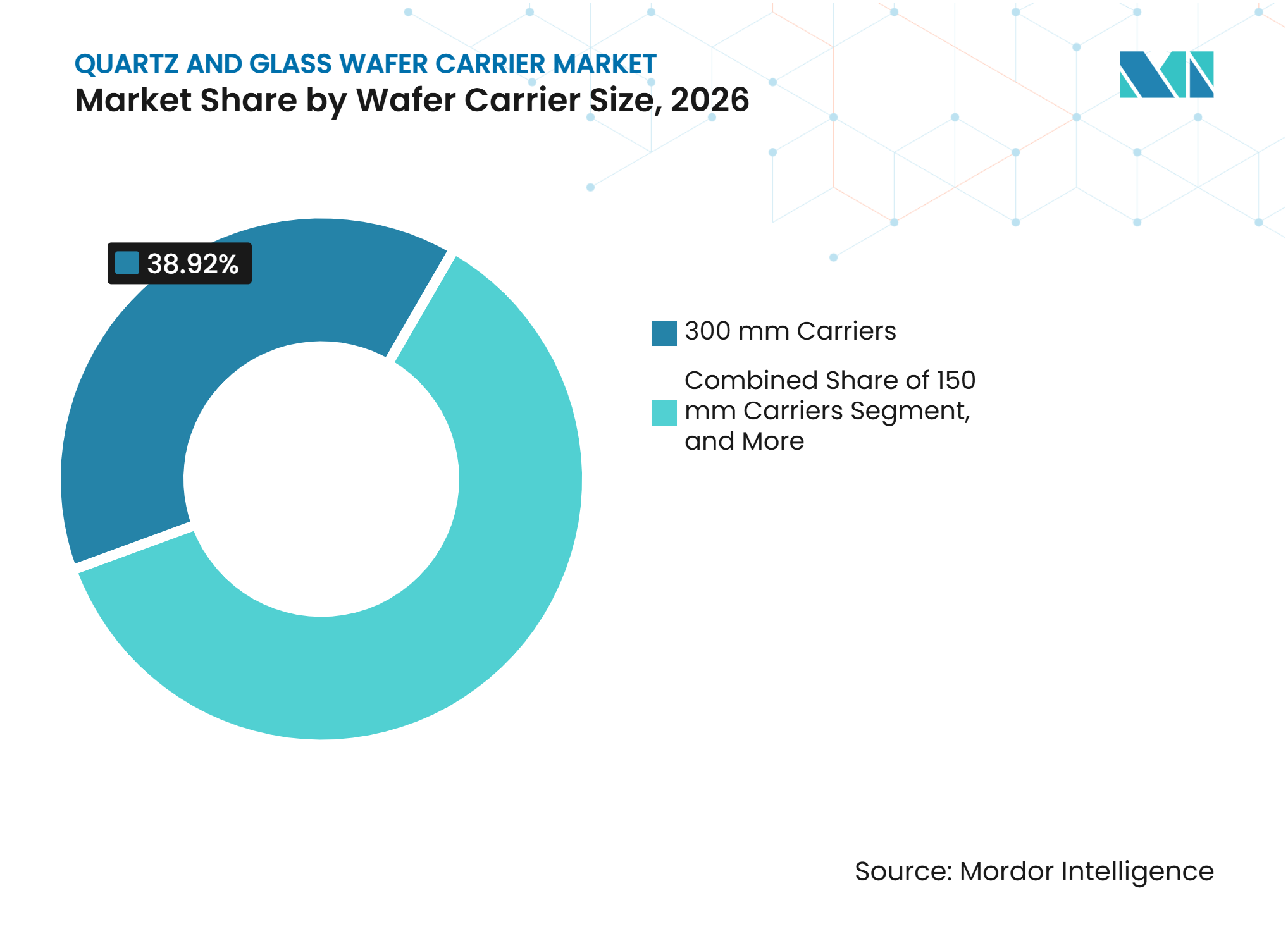
300 mm Formats Lead as Panel Formats AccelerateThe 300 mm segment held 38.92% of the Quartz and Glass Wafer Carrier Market share in 2026. It serves advanced logic, memory, and packaging operations that use the industry’s established large-wafer format. These carriers have demanding dimensional requirements because small deviations can affect wafer placement and process consistency across high-volume production tools. Synthetic high-purity grades are more important in advanced production settings that require tighter control of contamination and reliable lot-to-lot performance. The Quartz and Glass Wafer Carrier Market also relies on the 150 mm and 200 mm segments, which continue to support mature-node and power-semiconductor production.
Panel-format carriers are expected to expand at an 8.39% CAGR through 2032. Their momentum reflects the effort to increase packaging area beyond traditional round-wafer approaches. Larger panels require careful warpage management because thermal movement can affect alignment and yield across successive packaging stages. Scientific Reports has documented the relationship between carrier properties and warpage behavior in fan-out panel-level packaging.[4] This technical requirement favors suppliers that can maintain glass flatness, material consistency, and stable thermal performance at larger dimensions.
By End-Use Customer:
IDM Dominance Yields Ground to Emerging Fab TypesIDMs accounted for 36.47% of the Quartz and Glass Wafer Carrier Market share in 2026. Their demand is distributed across internal thermal processing, wafer fabrication, and advanced packaging operations, creating several recurring consumption points for these customers. This breadth can reduce exposure to changes in a single device category. IDMs also tend to use qualified supplier relationships across multiple component types and manufacturing sites. Their purchasing decisions emphasize predictable supply, established process performance, and technical support during equipment changes or process transitions.
Compound semiconductor fabs are projected to advance at a 10.59% CAGR through 2032. Their demand is linked to silicon carbide and gallium nitride devices used in power conversion and high-frequency applications. Foundries also remain important because advanced packaging services require both front-end quartzware and glass carriers for back-end processes. OSAT companies gain relevance as packaging programs move toward thinner wafers and larger panel formats. Research institutions and specialized device manufacturers remain small customers, but they can serve as early qualification sites for new glass compositions and carrier configurations.
Geography Analysis
Asia-Pacific
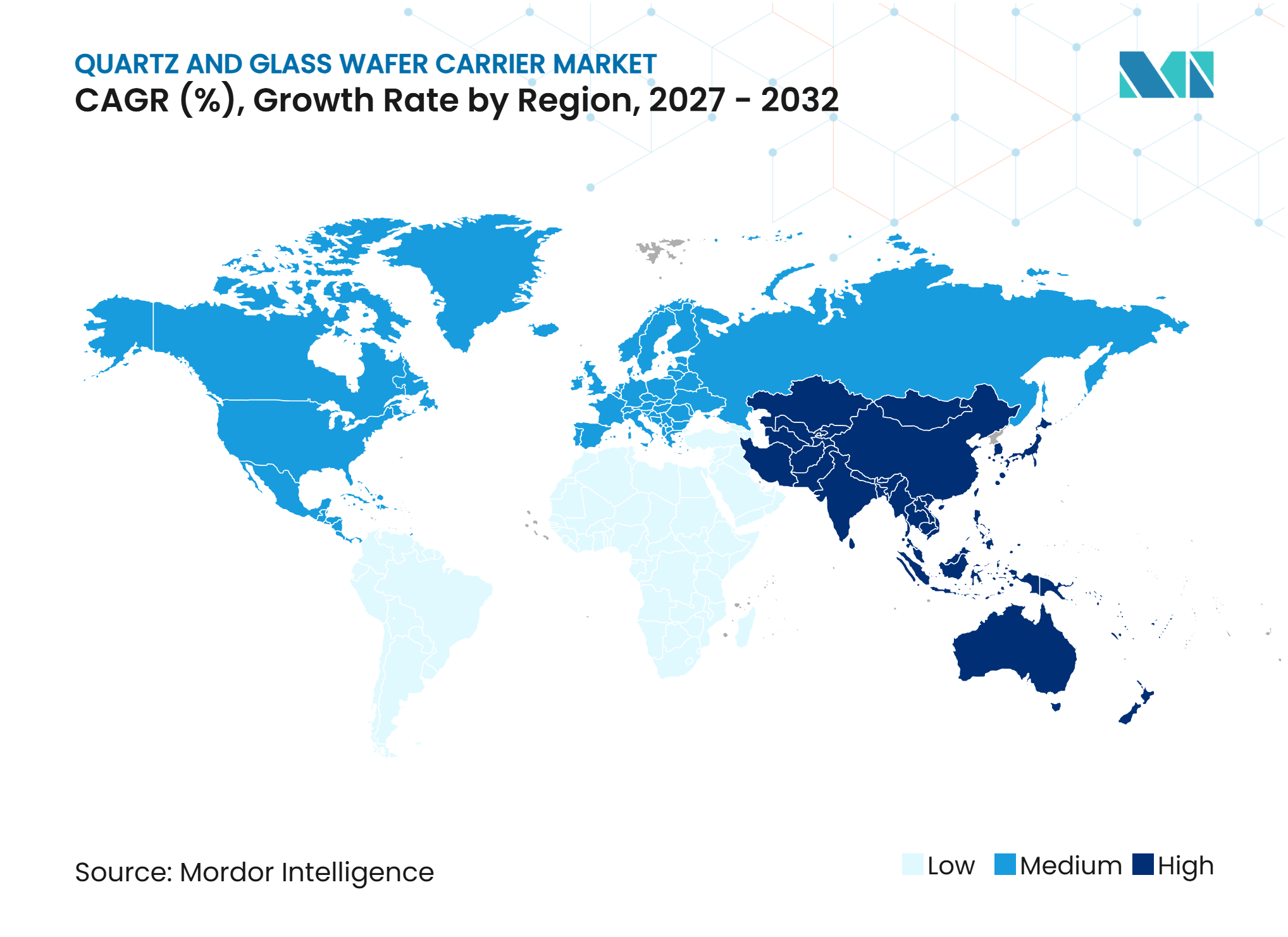
Asia-Pacific held 67.98% of the Quartz and Glass Wafer Carrier Market share in 2026 and is projected to record an 11.91% CAGR through 2032. The region combines a dense base of foundries, memory manufacturers, OSAT providers, and materials suppliers that support closely connected production networks. Taiwan supports demand through advanced logic and packaging activity, while South Korea adds memory and logic packaging requirements. Japan remains important for high-purity quartz and specialized glass manufacturing, supported by established expertise in high-specification material processing. The Quartz and Glass Wafer Carrier Market benefits from this regional concentration because component suppliers can work close to large fabrication and packaging customers. Advanced packaging programs also increase the need for qualified glass carriers alongside conventional quartzware.
North America
North America is seeing added demand from new front-end fab projects and related supplier investment. The United States CHIPS and Science Act supports semiconductor manufacturing capacity, which creates initial purchasing needs for process consumables and later replacement demand. Corning is investing USD 315 million in its Canton, New York facility, and federal support includes USD 32 million for the project. New 300 mm facilities need qualified quartz items during installation and recurring replacements after production begins, linking construction activity with continuing consumables demand. Customer proximity, delivery reliability, and domestic material capacity can therefore influence supplier selection.
Europe and Rest of the World
The Quartz and Glass Wafer Carrier Market in Europe has specialized demand from automotive and industrial semiconductor manufacturing, especially for power-device production. Germany is significant because SCHOTT supplies glass solutions for advanced semiconductor packaging and expanded its portfolio through the acquisition of QSIL GmbH. European policy support for semiconductor capacity can reinforce demand for process materials and specialized carriers. The Rest of the World includes Israel, Singapore, and Southeast Asian facilities that may gain importance as customers diversify supply chains. These locations have smaller current demand but may offer alternative procurement routes for qualified materials. Export controls and customer-specific material approvals will continue to shape sourcing decisions across these mixed geographies.
Competitive Landscape
Market Concentration
The Quartz and Glass Wafer Carrier Market includes established Japanese, German, Chinese, and other specialist manufacturers. Competition is based on certified purity, dimensional control, thermal stability, delivery performance, and the depth of customer qualification across specific manufacturing processes. Glass-carrier suppliers also differentiate through their ability to support thin-wafer handling and advanced packaging applications without compromising flatness or process stability. Supplier consolidation increased in 2025 when Heraeus combined its Conamic and Comvance businesses to create Heraeus Covantics. The company positions traceability from raw material through finished semiconductor products as a core capability.
SCHOTT completed the acquisition of QSIL GmbH in January 2025, strengthening its semiconductor materials portfolio. It also announced an accelerated expansion of its glass-carrier production capability at SEMICON Taiwan 2025. Heraeus Covantics opened a plant in Shenyang in March 2025 to produce high-purity and ultra-high-purity synthetic quartz products. These investments show that capacity, traceability, and product qualification remain central strategic priorities as customers seek dependable supply for advanced applications. Smaller and regional suppliers can compete in mature-node and mid-range applications, but advanced logic and memory customers maintain high technical and approval requirements.
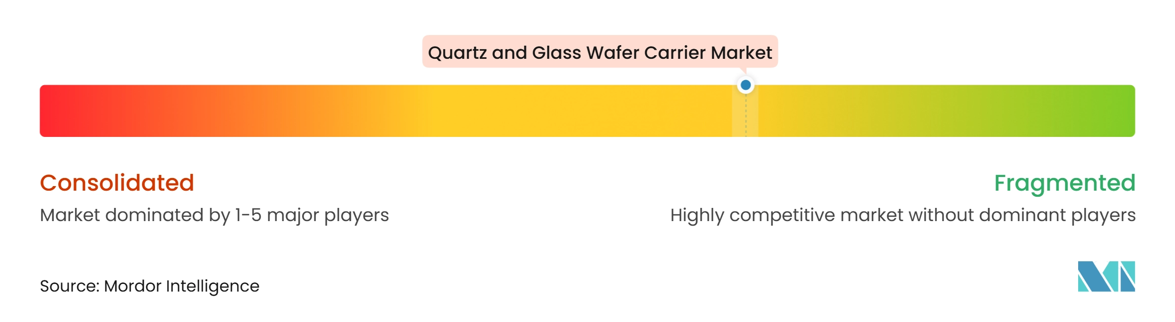
New opportunities in the Quartz and Glass Wafer Carrier Market are appearing in panel-format glass carriers and embedded glass substrates. These applications require suppliers to manage warpage, thermal expansion, and flatness across larger processing areas while meeting demanding handling and reliability expectations. The market remains concentrated in technically qualified suppliers, but the available top-player share does not support a precise market-wide concentration estimate across quartz and glass categories. Competitive outcomes will depend on the pace of packaging adoption, customer qualification results, and each supplier’s ability to scale without reducing material quality. Available eligible sources do not disclose a comparable combined market share for the leading suppliers across the full market.
Quartz and Glass Wafer Carrier Industry Leaders
-
Tosoh Quartz Inc.
-
Heraeus Conamic
-
Shin-Etsu Quartz Products
-
Hayward Quartz Technology
-
MARUWA Co., Ltd.
- *Disclaimer: Major Players sorted in no particular order
Quartz and Glass Wafer Carrier Market Companies Covered in this Report
- Tosoh Quartz Inc.
- Heraeus Conamic
- Shin-Etsu Quartz Products
- Hayward Quartz Technology
- Advanced Quartz Technology / DKEQ
- MARUWA Co., Ltd.
- Ferrotec Holdings Corporation
- Momentive Technologies
- QSIL SE
- Jiangsu Pacific Quartz Co., Ltd.
- Schunk Xycarb Technology
- SCHOTT AG
- Corning Incorporated
- AGC Inc.
- Ohara Corporation
- Plan Optik AG
- Nippon Electric Glass Co., Ltd.
- TOPPAN Holdings Inc.
- TECNISCO Ltd.
- Zhejiang Lante Optics Co., Ltd.
- Absolics Inc.
Recent Industry Developments in Quartz and Glass Wafer Carrier Market
- September 2026: At SEMICON Taiwan 2026, AUO Corporation and Corning jointly showcased a 510 × 515 mm glass-core substrate integrating Corning's semiconductor-grade glass with AUO's redistribution layer processes, targeting high-density interconnect and low-loss transmission requirements in AI server chips. AUO has committed NTD 8.6 billion (approximately USD 265 million) in capital expenditure covering through-glass via, RDL, and glass-core pilot lines; Chairman Paul Peng indicated that glass-core technology requires another two to three years to reach full maturity, positioning AUO-made glass panel carriers as a critical supply-chain link ahead of commercial scale-up.
- September 2026: SKC committed an additional KRW 92.1 billion (approximately USD 66.7 million) to its Absolics subsidiary for equipment upgrades aimed at improving glass-substrate production yields and quality, bringing SKC's total capital commitment to Absolics to KRW 373.1 billion (approximately USD 270 million). Absolics, which operates a glass-substrate plant in Covington, Georgia, is concurrently conducting semiconductor-package reliability evaluations with major U.S. semiconductor customers, with qualification completion expected to unlock mass-production orders.
- September 2026: Samsung Electro-Mechanics and Dongwoo Fine-Chem established GlaSSEM, a glass-core joint venture targeting glass-core substrate mass production in 2027. Samsung Electro-Mechanics is producing prototypes at its Sejong pilot line; the JV assigns substrate glass supply to Dongwoo Fine-Chem and packaging integration to Samsung Electro-Mechanics, creating a vertically coordinated supply chain that could reduce lead times for glass carrier and core substrate customers across AI and high-performance computing programs.
- July 2026: Intel and Lens Technology announced a strategic collaboration to advance glass-core-substrate advanced packaging, with industry observers expecting mass production to begin as early as the second half of 2027. In parallel, BOE deployed a fully automated glass-substrate pilot production line in the first half of 2026, completing development of 24-layer substrates exceeding 100 × 100 mm, and initiated customer validation testing with actual CPUs and GPUs, targeting an investment decision for a mass-production line by the first half of 2027.
Global Quartz and Glass Wafer Carrier Market Report Scope
The quartz and glass wafer carrier market comprises high-purity quartz, fused silica, borosilicate, and other specialty glass carriers, boats, cassettes, and holders used to support, position, transport, and process semiconductor wafers during fabrication and advanced packaging. These carriers provide thermal stability, chemical resistance, low contamination, and precise wafer spacing in applications such as diffusion, oxidation, annealing, CVD, lithography, wafer thinning, and temporary bonding.
The Quartz and Glass Wafer Carrier Market Report is Segmented by Product Type (Quartz Wafer Boats and Carriers, Glass Carrier Wafers, and Carrier Accessories), Process Application (Thermal Diffusion, Thermal Oxidation, Low-Pressure Chemical Vapor Deposition (LPCVD), Annealing, Wafer Thinning, Fan-Out Wafer-Level and Panel-Level Packaging (FO-WLP/FOPLP), 3D IC and Through-Silicon Via (TSV) Processing, and Compound Semiconductor Processing (SiC and GaN)), Wafer / Carrier Size (150 mm Carriers, 200 mm Carriers, 300 mm Carriers, and Panel-Format Carriers), End-Use Customer (Integrated Device Manufacturers (IDMs), Pure-Play Foundries, Outsourced Semiconductor Assembly and Test (OSAT) Companies, Compound Semiconductor Fabs, and Others End-Use Customer [MEMS, Specialty Device Manufacturers, and Research Institutions]), and Geography (North America, Europe, Asia-Pacific, and Rest of the World). The Market Forecasts are Provided in Terms of Value (USD).
Segmentation Overview
| Quartz Wafer Boats and Carriers |
| Glass Carrier Wafers |
| Carrier Accessories |
| Thermal Diffusion |
| Thermal Oxidation |
| Low-Pressure Chemical Vapor Deposition (LPCVD) |
| Annealing |
| Wafer Thinning |
| Fan-Out Wafer-Level and Panel-Level Packaging (FO-WLP/FOPLP) |
| 3D IC and Through-Silicon Via (TSV) Processing |
| Compound Semiconductor Processing (SiC and GaN) |
| 150 mm Carriers |
| 200 mm Carriers |
| 300 mm Carriers |
| Panel-Format Carriers |
| Integrated Device Manufacturers (IDMs) |
| Pure-Play Foundries |
| Outsourced Semiconductor Assembly and Test (OSAT) Companies |
| Compound Semiconductor Fabs |
| Others (MEMS, Specialty Device Manufacturers, and Research Institutions) |
| North America | United States |
| Canada | |
| Mexico | |
| Europe | Germany |
| United Kingdom | |
| France | |
| Italy | |
| Rest of Europe | |
| Asia-Pacific | China |
| Japan | |
| South Korea | |
| Taiwan | |
| India | |
| Rest of Asia-Pacific | |
| Rest of the World |
| By Product Type | Quartz Wafer Boats and Carriers | |
| Glass Carrier Wafers | ||
| Carrier Accessories | ||
| By Process Application | Thermal Diffusion | |
| Thermal Oxidation | ||
| Low-Pressure Chemical Vapor Deposition (LPCVD) | ||
| Annealing | ||
| Wafer Thinning | ||
| Fan-Out Wafer-Level and Panel-Level Packaging (FO-WLP/FOPLP) | ||
| 3D IC and Through-Silicon Via (TSV) Processing | ||
| Compound Semiconductor Processing (SiC and GaN) | ||
| By Wafer / Carrier Size | 150 mm Carriers | |
| 200 mm Carriers | ||
| 300 mm Carriers | ||
| Panel-Format Carriers | ||
| By End-Use Customer | Integrated Device Manufacturers (IDMs) | |
| Pure-Play Foundries | ||
| Outsourced Semiconductor Assembly and Test (OSAT) Companies | ||
| Compound Semiconductor Fabs | ||
| Others (MEMS, Specialty Device Manufacturers, and Research Institutions) | ||
| By Geography | North America | United States |
| Canada | ||
| Mexico | ||
| Europe | Germany | |
| United Kingdom | ||
| France | ||
| Italy | ||
| Rest of Europe | ||
| Asia-Pacific | China | |
| Japan | ||
| South Korea | ||
| Taiwan | ||
| India | ||
| Rest of Asia-Pacific | ||
| Rest of the World | ||
Key Questions Answered in the Report
What is the size of the Quartz and Glass Wafer Carrier Market?
The Quartz and Glass Wafer Carrier Market size is projected to expand from USD 310.21 million in 2026 and USD 332.20 million in 2027 to USD 471.19 million by 2032, registering a 7.09% CAGR over 2027-2032.
Which product category leads quartz and glass wafer carrier demand?
Quartz wafer boats and carriers lead the product category with 61.78% share in 2026, supported by recurring use in thermal processing and by customer requirements for clean, durable furnace components. Their installed base across diffusion, oxidation, and LPCVD operations supports continuing replacement needs.
Why are glass carrier wafers becoming more important?
Glass carrier wafers are projected to expand at an 8.26% CAGR as wafer thinning, temporary bonding, and fan-out packaging become more widely used in advanced packaging lines that require stable temporary support during processing. Their importance rises when thin substrates need controlled flatness through several thermal and mechanical steps.
Which process application has the highest share?
LPCVD holds the largest process application share at 26.59% in 2026 because it is widely used in logic, memory, and power-device deposition processes that continue to depend on thermally stable quartz components. Thermal diffusion and oxidation also maintain a steady base of quartzware consumption across established semiconductor process flows.
Which end-use customer is expected to expand fastest?
Compound semiconductor fabs are projected to record a 10.59% CAGR through 2032 as silicon carbide and gallium nitride production expands across power and high-frequency device applications. These facilities often require customer-specific carrier dimensions and materials that align with specialized reactor configurations.
Which region has the strongest position in wafer carrier demand?
Asia-Pacific holds 67.98% share in 2026 and is projected to record an 11.91% CAGR through 2032, supported by its concentration of fabs, packaging operations, and specialized materials suppliers. Taiwan, South Korea, Japan, and China collectively provide a dense customer base for both conventional quartzware and emerging glass carriers.