PCB X-Ray Inspection Systems Market Size and Share
Market Overview
| Study Period | 2020 - 2031 |
|---|---|
| Market Size (2026) | USD 2.86 Billion |
| Market Size (2031) | USD 4.46 Billion |
| Growth Rate (2026 - 2031) | 9.29 % |
| Fastest Growing Market | Asia-Pacific |
| Largest Market | Asia-Pacific |
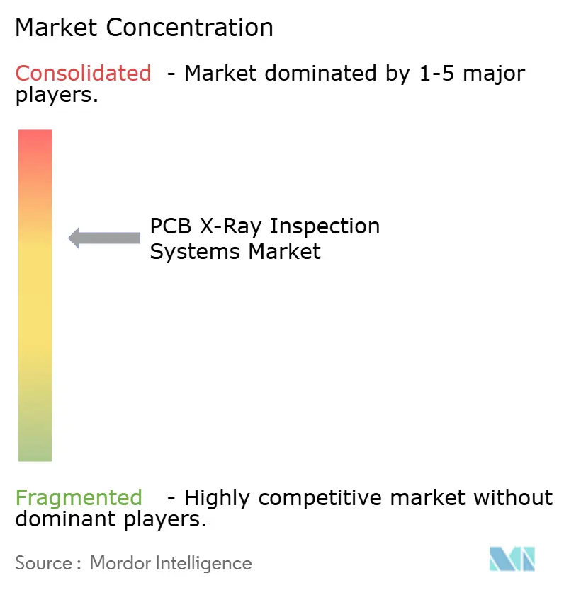
| Market Concentration | Medium |
Major Players *Disclaimer: Major Players sorted in no particular order Image © Mordor Intelligence. Reuse requires attribution under CC BY 4.0. | |
PCB X-Ray Inspection Systems Market Analysis by Mordor Intelligence
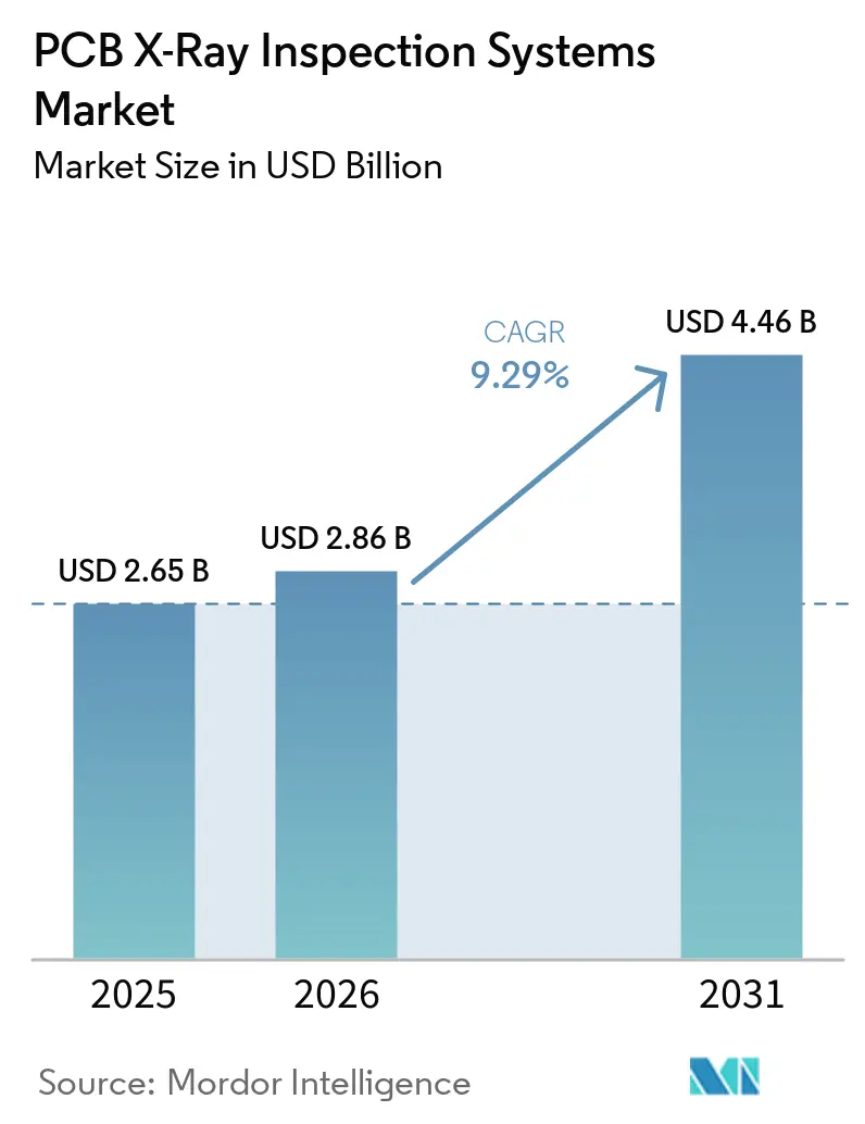
The PCB X-ray inspection systems market size was USD 2.65 billion in 2025, and USD 2.86 billion in 2026, and is forecast to reach USD 4.46 billion by 2031, registering a CAGR of 9.29% between 2026 and 2031. Demand is tied to the need to inspect concealed solder joints and internal structures in denser electronic assemblies. Optical methods cannot verify these features once component packages cover the joints. Smaller board layouts, electric vehicle power electronics, and software-based defect classification are broadening the role of automated X-ray inspection beyond traditional solder-joint screening. Asia-Pacific accounted for 48.63% of revenue in 2025 because China, South Korea, Japan, and Southeast Asia remain major electronics manufacturing locations. Vendors are responding by combining imaging systems with production-line software, while manufacturers are seeking systems that can support quality control and process improvement.
Key Report Takeaways
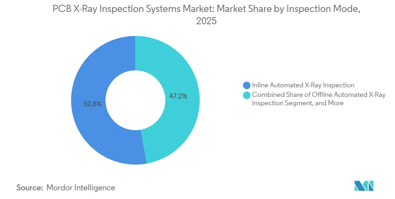
- By inspection mode, inline automated X-ray inspection held 52.84% of revenue in the PCB X-ray inspection systems market in 2025, while offline automated X-ray inspection is projected to expand at a CAGR of 12.46% through 2031.
- By imaging dimension, 2D X-ray inspection accounted for 57.36% of revenue in 2025, while 3D computed tomography inspection is projected to grow at a CAGR of 11.74% through 2031.
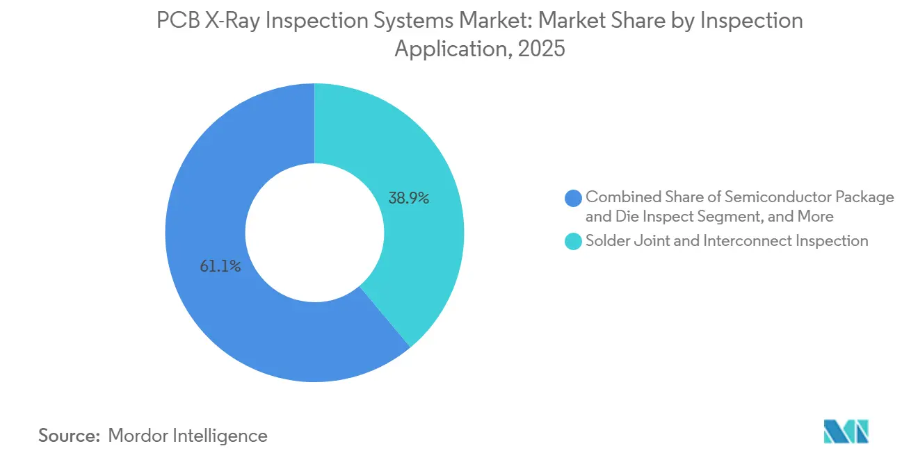
- By inspection application, solder joint and interconnect inspection held 38.92% of revenue in 2025, while semiconductor package and die inspection is expected to expand at a CAGR of 11.56% through 2031.
- By end-user industry, consumer electronics held 36.47% of the PCB X-ray inspection systems market revenue in 2025, while automotive electronics is projected to record a CAGR of 11.83% through 2031.
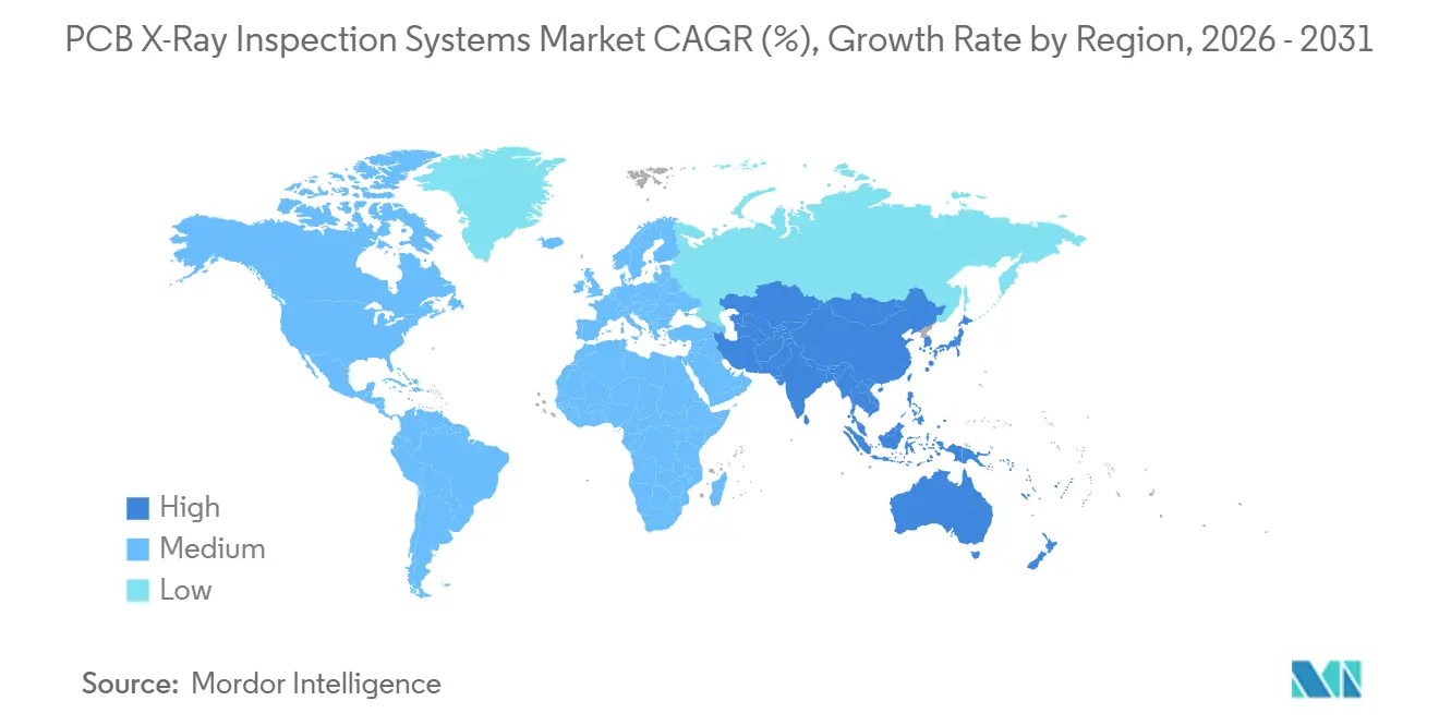
- By geography, Asia-Pacific accounted for 48.63% of the PCB X-ray inspection systems market revenue in 2025 and is expected to grow at a CAGR of 12.12% through 2031.
Note: Market size and forecast figures in this report are generated using Mordor Intelligence’s proprietary estimation framework, updated with the latest available data and insights as of January 2026.
Global PCB X-Ray Inspection Systems Market Trends and Insights
Drivers Impact Analysis*
| DRIVER | (~) % IMPACT ON CAGR FORECAST | GEOGRAPHIC RELEVANCE | IMPACT TIMELINE |
|---|---|---|---|
| Rising Miniaturization and Higher Component Densities | +2.5% | Global, most pronounced in Asia-Pacific and North America | Short term (≤ 2 years) |
| Growth in Automotive Electronics and Electric Vehicles | +2% | North America, Europe, and China | Medium term (2-4 years) |
| AI-Enabled Defect Classification and Reduced False Calls | +1.5% | Global, with early-mover activity in Asia-Pacific and North America | Medium term (2-4 years) |
| Expansion of Industry 4.0 and Connected Manufacturing Lines | +1.2% | Europe, North America, and advanced Asia-Pacific clusters | Medium term (2-4 years) |
| Proliferation of Advanced Packaging and Chiplet Architectures | +0.9% | Asia-Pacific, including Taiwan, South Korea, and Japan, and North America | Long term (≥ 4 years) |
| Expansion of High-Reliability Electronics Manufacturing in Asia-Pacific | +0.7% | Asia-Pacific, with spillover to South and Southeast Asia | Medium term (2-4 years) |
| Source: Mordor Intelligence | |||
Rising Miniaturization and Higher Component Densities
Smaller PCB layouts are increasing the use of PCB X-ray inspection systems market systems for internal quality checks. This PCB X-ray inspection systems market demand rises when assembly designs leave critical joints concealed beneath packages. Ball-grid array, quad-flat no-lead, and land-grid array packages conceal their solder connections beneath the component body. This makes non-destructive X-ray inspection necessary where optical equipment cannot view the joint. Demand becomes more acute as package pitches move toward 0.3 mm and below. Buyers of power modules are also asking for measured void percentages rather than pass or fail results. This favors 3D CT systems that can report void volume and support more detailed supplier requirements.
Growth in Automotive Electronics and Electric Vehicles
Automotive electronics is shifting automated X-ray inspection from a routine assembly check toward safety-related verification. The PCB X-ray inspection systems market therefore serves both supplier quality records and production-line controls. ADAS sensor modules, battery-management PCBs, and SiC inverter modules require consistent solder quality at high throughput. OMRON introduced the VT-X850 3D CT automated X-ray inspection system for power modules, e-axle assemblies, and inverters used in electric vehicle drivetrains.[1]OMRON Corporation, “OMRON VT-X850 AXI: 3D CT Automated X-ray Inspection System for EV Production Environments,” ETEK Europe, etek-europe.com. IATF 16949:2016 requires documented statistical process control for automotive joining processes, and inspection data can support that documentation. European vehicle makers can specify these controls, while many tier-2 suppliers operate in Southeast Asia. This places additional demand on electronics factories in ASEAN production clusters.
AI-Enabled Defect Classification and Reduced False Calls
False calls add operator time and can expose boards to needless rework. Automated classification can separate actual defects from acceptable process variation at a faster rate than manual review. The PCB X-ray inspection systems market is benefiting as buyers seek more dependable defect decisions without adding review staff. Viscom introduced vAI ProVision at Productronica 2025 to generate and optimize 3D automated X-ray inspection programs with limited manual work.[2]Viscom SE, “Viscom Introduces AI-Powered Fast Program Generation vAI ProVision at productronica 2025,” Viscom, viscom.com. ViTrox reported that its V810Ai QX1 Smart 3D AXI system reached up to 95% accuracy in autonomous defect buy-off using its AI VVTS feature. A 2025 peer-reviewed study of a GAN-YOLOv8n model for SMT resistor AXI images reported 92.9% mean average precision at an intersection-over-union threshold of 0.5. Such results support greater use of automated review in lower-risk inspection settings.
Expansion of Industry 4.0 and Connected Manufacturing Lines
Connected manufacturing is changing how factories evaluate automated X-ray inspection investments. The PCB X-ray inspection systems market is increasingly tied to systems that produce usable process data rather than isolated defect images. An inspection system can send information to manufacturing execution systems and guide upstream process adjustments. These adjustments can include stencil apertures, reflow profiles, and solder-paste volume targets. Lumafield reported in 2026 that 77% of manufacturers still used manual visual inspection, while nearly half devoted up to 10% of production labor hours to manual checks. IPC-CFX-2591 and IPC-HERMES-9852 enable inspection outputs to move between automated X-ray inspection equipment and upstream SMT systems. EMS providers serving smart-factory customers can therefore use connected inspection to improve yields as well as contain defects.
Restraints Impact Analysis*
| RESTRAINT | (~) % IMPACT ON CAGR FORECAST | GEOGRAPHIC RELEVANCE | IMPACT TIMELINE |
|---|---|---|---|
| High Initial Capital Investment and Long Payback Periods | -1.5% | Global, most acute in South and Southeast Asia and South America | Short term (≤ 2 years) |
| Shortage of Skilled AXI and CT Programming Personnel | -0.9% | Global, most severe in emerging electronics manufacturing clusters | Medium term (2-4 years) |
| Integration Complexity Across Legacy SMT Lines | -0.6% | Europe and North America, where the installed base is older | Medium term (2-4 years) |
| Radiation Safety, Calibration, and Compliance Costs | -0.4% | Global, with stricter enforcement in the European Union, North America, and Japan | Long term (≥ 4 years) |
| Source: Mordor Intelligence | |||
High Initial Capital Investment and Long Payback Periods
Full-featured 3D CT systems cost from USD 300,000 to USD 1 million. These outlays can place the payback period beyond the planning horizon of mid-sized manufacturers and subcontractors. A manufacturer may need to choose between a shared high-capability system and several lower-capability units. Lumafield reported that inspection-cost concerns remained a leading reason for retaining manual programs, despite defect escapes and rework costs. Large OEMs and EMS providers can deploy advanced systems, while many smaller facilities remain underpenetrated. Modular, subscription-based, and lower-capital systems may address this gap without requiring full CT capability.
Shortage of Skilled AXI and CT Programming Personnel
3D CT recipe development requires knowledge of X-ray physics, image reconstruction artifacts, and component failure modes. These skills are limited in many regions and are especially scarce in growing manufacturing centers in India, Vietnam, and Mexico. Shortages can delay upgrades for smaller factories that cannot support dedicated inspection engineers. They also concentrate on advanced automated X-ray inspection capability among larger tier-1 operators. OMRON announced plans to integrate its 3D CT systems with NVIDIA Omniverse and Metropolis AI libraries in 2026 to reduce reliance on specialist defect-judgment work. Systems that simplify programming can lower a practical barrier to wider adoption.
*Our forecasts treat driver/restraint impacts as directional, not additive. The impact forecasts reflect baseline growth, mix effects, and variable interactions.
Segment Analysis
By Inspection Mode: Offline Systems Gain Ground in High-Mix, Low-Volume Manufacturing
Inline automated X-ray inspection held 52.84% of 2025 revenue, reflecting its role in high-volume consumer electronics and automotive assembly. These systems provide defect feedback at conveyor speed for factories operating continuous production schedules. Offline automated X-ray inspection is projected to expand at a CAGR of 12.46% through 2031. Contract manufacturers serving aerospace, medical, and defense customers use offline systems when flexibility and high resolution are more important than line throughput. Manual and benchtop equipment remains relevant for prototype evaluation, failure analysis, research and development, and job-shop work. Lumafield launched the Mars in-line arrayed X-ray system in July 2026 with 2D and 2.5D inspection at speeds of up to 760 mm/s.
The PCB X-ray inspection systems market size for inline equipment reflects demand for integration into high-throughput production lines. The PCB X-ray inspection systems market also includes offline systems for high-mix programs that require flexible inspection outside those lines. Dynamic planar CT acquisition is narrowing the historic trade-off between inline speed and offline resolution. This could enable inline CT use in applications that previously relied on batch sampling. Suppliers that offer dual-mode capability can serve both production needs with fewer system compromises. Pure offline specialists may face pressure as these capabilities become available in broader product portfolios.



By Imaging Dimension: 3D CT Expands into Semiconductor Applications
2D X-ray inspection accounted for 57.36% of 2025 revenue because it remains cost-effective for standard PCB solder-joint checks. The PCB X-ray inspection systems market share held by 2D systems reflects their ability to resolve many planar defects without CT processing. 3D computed tomography inspection is projected to grow at a CAGR of 11.74% through 2031. Automotive power electronics needs measured void information, while semiconductor producers need to inspect stacked die interconnects. Rayence expanded its Flash Series detector platform in March 2026 to support inline inspection and 3D CT on AI chips and HBM. The platform offered a 49.5 µm pixel size and up to 70 frames per second.
2.5D X-ray inspection remains a middle option between planar imaging and full CT. It suits BGA void mapping and through-silicon-via analysis, where angled images add depth information. The PCB X-ray inspection systems market is moving toward greater capability differences among suppliers. Comet Yxlon enhanced its FF35 CT in 2026 with a 160 kV nanofocus tube for advanced semiconductor-package inspection. Suppliers with microfocus and nanofocus source technology can differentiate in advanced packaging work. Vendors focused chiefly on throughput and system price may face more pressure where 3D CT becomes a standard tender requirement.
By Inspection Application: Semiconductor Packaging Pulls Inspection Upstream
Solder joint and interconnect inspection accounted for 38.92% of 2025 inspection-application revenue. The segment remains important because BGA, QFN, and LGA joints cannot be verified by optical equipment alone. IPC-A-610 criteria for concealed joints can increasingly be supported with automated X-ray inspection data. Semiconductor package and die inspection is projected to grow at a CAGR of 11.56% through 2031. Advanced packages use 2.5D interposers, 3D stacked dies, and chiplet modules that require inspection at wafer and die-attach stages. ZEISS states that its NLX system supports in-line 3D X-ray laminography at the 300 mm wafer level for TSVs, microbumps, and stacked dies.[3]ZEISS SMT, “NLX: In-line 3D X-ray Laminography at 300 mm Wafer Level,” ZEISS, zeiss.com.
The PCB X-ray inspection systems market size for semiconductor applications is supported by inspection needs that occur before final assembly. Through-hole, via, and internal-structure inspection serve aerospace and power-electronics work where internal geometry is important. Structural-defect and foreign-material detection also support specialized quality programs. Component presence and placement checks can move from optical tools to X-ray systems when shadowing makes visual confirmation unreliable. Nidec Advance Technology and Techno Horizon signed a March 2026 agreement to develop a system for AI-server multilayer PCB back-drill inspection. This work shows how specific assembly designs can create new inspection uses.
By End-User Industry: Automotive Electronics Changes Demand Patterns
Consumer electronics held 36.47% of 2025 end-user revenue because of the large production volumes for smartphones, tablets, wearables, and connected-home devices. Automotive electronics is projected to expand at a CAGR of 11.83% through 2031. Electric drivetrain systems and ADAS integration are driving this demand. Automotive buyers need void percentages measured against acceptance criteria rather than a simple visual outcome. IPC-7095D commonly uses a 25% limit for BGA voiding in the cited application context. This requirement favors 3D CT over conventional 2D imaging in complex power modules.
Consumer electronics remained the largest end-user revenue contributor in 2025 because of the large production volumes for smartphones, tablets, wearables, and connected-home devices. Industrial and energy electronics are also growing uses for power converters, motor drives, and renewable-energy inverters. The PCB X-ray inspection systems market is also relevant to aerospace, defense, and medical electronics, which form a smaller but high-value customer group. AS9100D and ISO 13485 documentation needs make inspection records part of an audit trail for these applications. EMS providers are investing in inspection-as-a-service to serve OEM customers that cannot justify their own equipment. This approach can extend X-ray inspection access beyond direct OEM installations.
Geography Analysis
Asia-Pacific accounted for 48.63% of automated X-ray inspection revenue in 2025 and is projected to record a CAGR of 12.12% through 2031. The PCB X-ray inspection systems market in the region combines a large electronics production base with ongoing equipment upgrades. China, South Korea, and Japan support demand from semiconductor packaging and automotive electronics. Vietnam, Thailand, and Malaysia are entering a period of investment as production shifts from China’s coastal manufacturing areas. Regional vendors can compete through local application support and pricing. ViTrox, headquartered in Penang, illustrates the presence of locally based suppliers in this environment.
North American demand in the PCB X-ray inspection systems market is increasingly tied to AI accelerators, high-performance computing processors, memory packaging, and battery-cell manufacturing. These applications can require inline CT inspection and specialized semiconductor inspection. Nordson Test and Inspection opened a Center of Excellence in Phoenix in August 2026 to provide demonstrations and training for its inspection platforms. Viscom reported EUR 55.715 million in H1 2026 order intake, equivalent to USD 61.3 million at the reported average H1 2026 exchange rate, and identified North America as a strong demand region. Europe is supported by vehicle makers and tier-1 suppliers in Germany, France, and Italy. ZEISS launched the OMNIA GC 220-180 in July 2025 for automated 2D inspection of large automotive aluminum castings.
South America, the Middle East, and Africa remain earlier-stage PCB X-ray inspection systems markets. The PCB X-ray inspection systems market in these areas is supported by distinct automotive, industrialization, and maintenance requirements. Brazil has the region’s clearest opportunity because of automotive electronics and export-focused suppliers. The United Arab Emirates and Saudi Arabia are building electronics capacity through industrialization programs. Africa’s manufacturing base remains limited, so near-term use is focused on imported equipment for mining, oil and gas, and telecommunications electronics maintenance. India is gaining attention as local electronics output expands. Koh Young opened a branch office in Noida during 2026, but its cited activity concerned optical inspection solutions rather than commercial automated X-ray inspection systems.

Competitive Landscape
The PCB X-ray inspection systems market is moderately consolidated among large suppliers and fragmented across the middle tier. ViTrox Corporation Berhad, Nordson Corporation, and Viscom SE together held 27% of global revenue in 2025. Suppliers compete on resolution, CT speed, software integration, application coverage, and service presence. Their portfolios can focus on SMT inspection, semiconductor work, or multiple materials and use cases. OMRON’s reported 2026 work to integrate 3D CT systems with NVIDIA software shows how suppliers are seeking to add software-based differentiation. A U.S. patent for an AI-assisted dual-indicator X-ray method also points to increased intellectual-property activity in automated decision support.[4]United States Patent and Trademark Office, “Systems and Methods for Automated X-ray Inspection, US Patent 12298258,” United States Patent and Trademark Office, exa.ai.
The PCB X-ray inspection systems market has an opportunity in lower-cost modular systems for mid-sized manufacturers. These customers may not support the cost of conventional CT equipment. Lumafield introduced Mars in July 2026 as a cloud-connected arrayed 2D and 2.5D system for full production inspection. Another opportunity is inspection of X-ray-sensitive DRAM, HBM, and advanced-node logic devices. These components can require low-dose source and detector designs because full CT protocols may not be suitable. Nidec Advance Technology and Techno Horizon’s development agreement addresses a specialized requirement for automated AI-server PCB back-drill inspection.
Safety certification and regulatory compliance can limit entry for new suppliers. IEC 61010-1 requirements and national radiation-safety rules favor vendors with established compliance capabilities. Larger providers can also provide training and local applications support alongside the equipment. Nordson’s Phoenix facility is one example of investment in demonstration and customer training. Viscom’s vAI ProVision is another example, as it reduces inspection-program setup work for 3D systems. These moves place greater value on software, support, and application knowledge in the PCB X-ray inspection systems market.
PCB X-Ray Inspection Systems Industry Leaders
Viscom SE
Nordson Corporation
Comet Yxlon GmbH
Nikon Metrology, Inc.
Waygate Technologies GmbH
- *Disclaimer: Major Players sorted in no particular order

Recent Industry Developments
- August 2026: Nordson Test and Inspection opened a purpose-built Centre of Excellence in Phoenix, Arizona, housing its full AXI, optical, and acoustic inspection portfolio alongside WaferSense semiconductor metrology sensors. The facility provides customers full demonstration and training capability before capital commitment, supporting informed pre-purchase evaluation in the semiconductor and SMT inspection markets.
- July 2026: Lumafield launched Mars, a high-speed in-line arrayed X-ray system offering 100% production inspection at up to 760 mm/s, available in 2D and 2.5D configurations with cloud-connected Voyager software for AI-driven automated decisions and real-time process monitoring. The launch was underpinned by Lumafield's 2026 Cost of Quality Report, which found that 77% of manufacturers still relied on manual visual inspection.
- March 2026: Nidec Advance Technology and Techno Horizon signed a joint development contract to build an AXI system for automated back-drill inspection of AI-server and datacenter multilayer PCBs, targeting total mass-production inspection speed with automated OK/defect judgment for stab-length measurement.
- March 2026: Rayence expanded its Flash Series CMOS X-ray detector platform for semiconductor AXI and 3D CT applications, achieving 49.5 µm pixel size and up to 70 frames per second to support inline inspection of AI chips and HBM at scale, with long-term supply agreements established with global top-tier AXI and CT system manufacturers.


Global PCB X-Ray Inspection Systems Market Report Scope
The PCB X-ray inspection systems market comprises automated X-ray imaging and computed tomography (CT) equipment used to detect internal defects, measure dimensional accuracy, and verify assembly quality in printed circuit boards (PCBs) and electronic assemblies. These systems employ 2D/3D X-ray imaging, real-time radiography, and AI-powered image analysis to identify solder joint voids, component misalignment, hidden cracks, delamination, and short circuits beneath surface layers without destructive testing, enabling manufacturers to maintain yield rates, reduce rework, and ensure reliability compliance for high-density interconnect (HDI) PCBs, automotive electronics, aerospace systems, and consumer devices where internal structural integrity is critical to performance and safety.
The PCB X-Ray Inspection Systems Market Report is Segmented by Inspection Mode (Inline Automated X-Ray Inspection, Offline Automated X-Ray Inspection, and Manual and Benchtop X-Ray Inspection), Imaging Dimension (2D X-Ray Inspection, 2.5D X-Ray Inspection, and 3D Computed Tomography Inspection), Inspection Application (Solder Joint and Interconnect Inspection, Through-Hole, Via, and Internal Structure Inspection, Semiconductor Package and Die Inspection, Component Presence, Placement, and Verification, and Structural Defect and Foreign-Material Detection), End-User Industry (Consumer Electronics, Automotive Electronics, Industrial and Energy Electronics, Aerospace and Defense Electronics, Medical Electronics, Telecommunications and Networking Equipment, Electronics Manufacturing Services Providers, and Other End-User Industries), and Geography. The Market Forecasts are Provided in Terms of Value (USD).
| Inline Automated X-Ray Inspection |
| Offline Automated X-Ray Inspection |
| Manual and Benchtop X-Ray Inspection |
| 2D X-Ray Inspection |
| 2.5D X-Ray Inspection |
| 3D Computed Tomography Inspection |
| Solder Joint and Interconnect Inspection |
| Through-Hole, Via, and Internal Structure Inspection |
| Semiconductor Package and Die Inspection |
| Component Presence, Placement, and Verification |
| Structural Defect and Foreign-Material Detection |
| Consumer Electronics |
| Automotive Electronics |
| Industrial and Energy Electronics |
| Aerospace and Defense Electronics |
| Medical Electronics |
| Telecommunications and Networking Equipment |
| Electronics Manufacturing Services Providers |
| Other End-User Industries |
| North America | United States | |
| Canada | ||
| Mexico | ||
| South America | Brazil | |
| Argentina | ||
| Rest of South America | ||
| Europe | Germany | |
| United Kingdom | ||
| France | ||
| Italy | ||
| Spain | ||
| Rest of Europe | ||
| Asia-Pacific | China | |
| Japan | ||
| India | ||
| South Korea | ||
| ASEAN | ||
| Rest of Asia-Pacific | ||
| Middle East and Africa | Middle East | Saudi Arabia |
| United Arab Emirates | ||
| Turkey | ||
| Rest of the Middle East | ||
| Africa | South Africa | |
| Nigeria | ||
| Rest of Africa | ||
| By Inspection Mode | Inline Automated X-Ray Inspection | ||
| Offline Automated X-Ray Inspection | |||
| Manual and Benchtop X-Ray Inspection | |||
| By Imaging Dimension | 2D X-Ray Inspection | ||
| 2.5D X-Ray Inspection | |||
| 3D Computed Tomography Inspection | |||
| By Inspection Application | Solder Joint and Interconnect Inspection | ||
| Through-Hole, Via, and Internal Structure Inspection | |||
| Semiconductor Package and Die Inspection | |||
| Component Presence, Placement, and Verification | |||
| Structural Defect and Foreign-Material Detection | |||
| By End-User Industry | Consumer Electronics | ||
| Automotive Electronics | |||
| Industrial and Energy Electronics | |||
| Aerospace and Defense Electronics | |||
| Medical Electronics | |||
| Telecommunications and Networking Equipment | |||
| Electronics Manufacturing Services Providers | |||
| Other End-User Industries | |||
| By Geography | North America | United States | |
| Canada | |||
| Mexico | |||
| South America | Brazil | ||
| Argentina | |||
| Rest of South America | |||
| Europe | Germany | ||
| United Kingdom | |||
| France | |||
| Italy | |||
| Spain | |||
| Rest of Europe | |||
| Asia-Pacific | China | ||
| Japan | |||
| India | |||
| South Korea | |||
| ASEAN | |||
| Rest of Asia-Pacific | |||
| Middle East and Africa | Middle East | Saudi Arabia | |
| United Arab Emirates | |||
| Turkey | |||
| Rest of the Middle East | |||
| Africa | South Africa | ||
| Nigeria | |||
| Rest of Africa | |||


Key Questions Answered in the Report
What is the automated X-ray inspection market size?
The PCB X-ray inspection systems market size was USD 2.65 billion in 2025, and USD 2.86 billion in 2026, and is forecast to reach USD 4.46 billion by 2031, registering a CAGR of 9.29% between 2026 and 2031.
What is driving automated X-ray inspection adoption?
Denser electronic assemblies, concealed solder joints, electric vehicle power modules, and connected manufacturing lines are expanding use of X-ray inspection.
Which inspection mode is growing fastest?
Offline automated X-ray inspection is projected to grow at a CAGR of 12.46% through 2031, supported by high-mix and low-volume manufacturing needs.
Why is 3D CT becoming more important for electronics inspection?
3D CT can measure voids and inspect stacked die structures that are difficult to assess with conventional 2D imaging.
Which end-user application has the strongest growth outlook?
Automotive electronics is projected to grow at a CAGR of 11.83% through 2031, supported by EV power electronics and ADAS systems.
Which region leads demand for automated X-ray inspection?
Asia-Pacific held 48.63% of revenue in 2025 and is projected to grow at a CAGR of 12.12% through 2031.
Page last updated on: