
Size and Share of North America Solder Materials Market In Semiconductor Industry
Market Overview
| Study Period | 2021 - 2032 |
|---|---|
| Forecast Data Period | 2027 - 2032 |
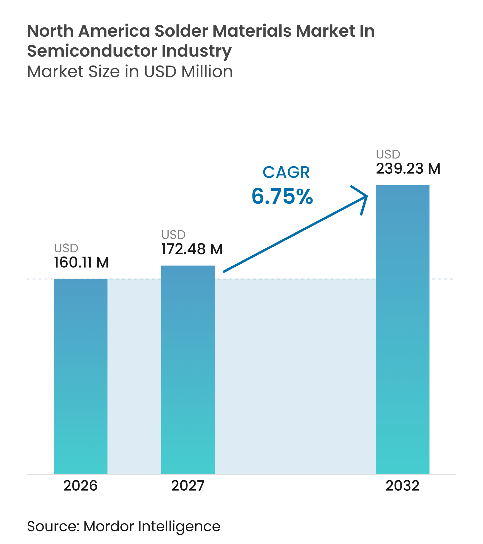
| Base Year Market Size (2026) | USD 160.11 Million |
| Market Size (2027) | USD 172.48 Million |
| Market Size (2032) | USD 239.23 Million |
| Growth Rate (2027 - 2032) | 6.75 % |
| Market Concentration | Medium |
Major Players *Disclaimer: Major Players sorted in no particular order Image © Mordor Intelligence. Reuse requires attribution under CC BY 4.0. | |
Analysis of North America Solder Materials Market In Semiconductor Industry by Mordor Intelligence
The North America solder materials market in semiconductor industry size is projected to expand from USD 160.11 million in 2026 to USD 239.23 million by 2032, registering a CAGR of 6.75% between 2027 to 2032. Demand is being shaped by denser semiconductor packages, which require more interconnects and tighter control of voiding, pitch, and alloy performance. Advanced packaging, high-performance computing, and power devices are raising the material requirements for paste, balls, preforms, and fluxes. Domestic manufacturing investment is also increasing the value of local qualification, technical support, and dual sourcing. Suppliers that combine alloy design with application engineering are better placed to serve facilities that must meet supply-chain and quality requirements. In the North America solder materials market in semiconductor industry, raw-material prices and the shift toward alternative interconnect technologies remain material constraints.
Key Report Takeaways
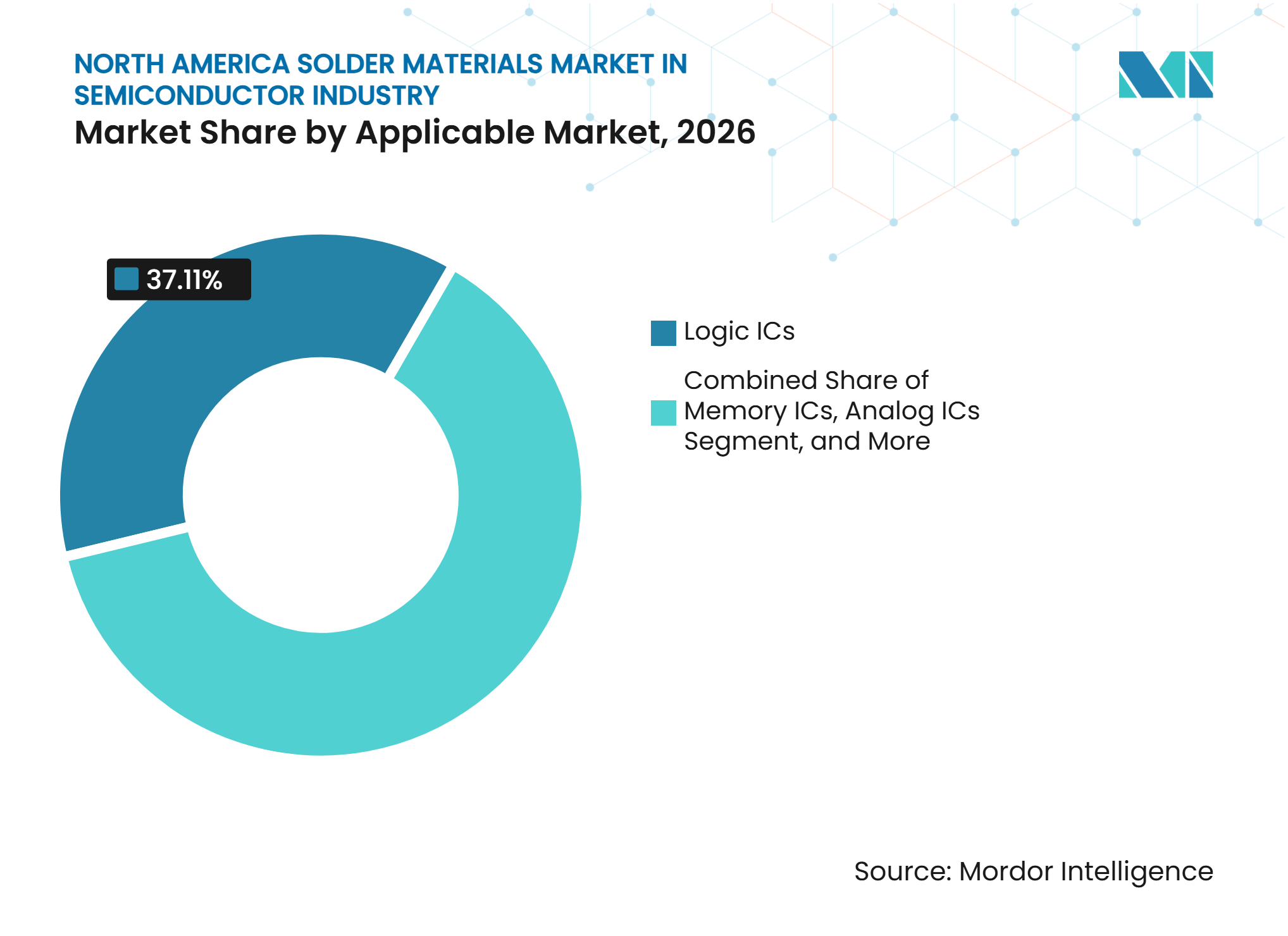
- By applicable market, logic ICs held 37.11% of the North America solder materials market in semiconductor industry share in 2026 and are projected to expand at a 7.11% CAGR through 2032.
- By product form, solder paste accounted for 33.12% of the North America solder materials market share in 2026, while solder preforms are expected to expand at a 7.23% CAGR through 2032.
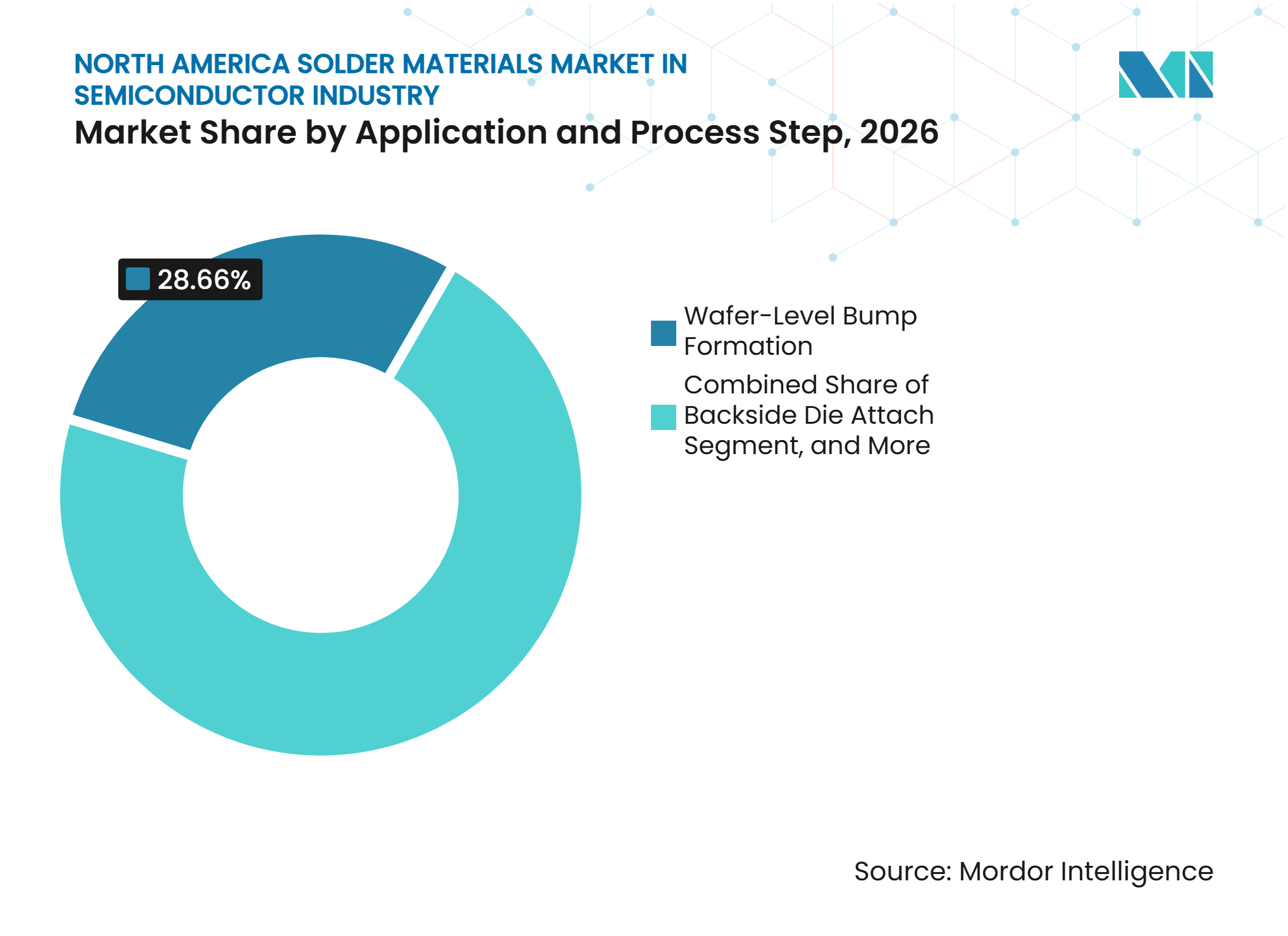
- By application and process step, wafer-level bump formation commanded 28.66% of the North America solder materials market size in 2026 and is projected to advance at a 7.42% CAGR through 2032.
- By geography, the United States held 84.33% of market value in 2026, while Mexico is expected to expand at a 7.33% CAGR through 2032.
Note: Market numbers in this report are based on Mordor Intelligence's proprietary estimation framework, which combines nine months of actuals with Q4 projections for base year 2026.
Market Trends and Insights
Drivers Impact Analysis of North America Solder Materials Market In Semiconductor Industry*
| Driver | (~) % Impact on CAGR Forecast | Geographic Relevance | Impact Timeline |
|---|---|---|---|
| Rising Advanced Packaging and Heterogeneous Integration Demand | +2.0% | Global, concentrated in the United States, Arizona, Texas, Ohio, and New York | Medium term (2-4 years) |
| Growing AI, High-Performance Computing, and Data-Center Semiconductor Production | +1.5% | United States and Canada, with spillover to Mexico | Short term (≤ 2 years) |
| Increasing Automotive Electrification and Power Semiconductor Content | +1.1% | United States and Mexico automotive Tier 1 clusters | Medium term (2-4 years) |
| North American Semiconductor Manufacturing and Packaging Localization | +0.9% | United States and Mexico, with early gains in Arizona, Texas, and Jalisco | Long term (≥ 4 years) |
| Growth of Low-Temperature and Low-Carbon Soldering Processes | +0.5% | Global, led by North American OSAT and IDM facilities | Medium term (2-4 years) |
| Rising Demand for Ultra-Fine-Pitch and Low-Voiding Interconnect Materials | +0.4% | United States, with spillover to Canadian photonics clusters in Ontario and Quebec | Long term (≥ 4 years) |
| Source: Mordor Intelligence | |||
Rising Advanced Packaging and Heterogeneous Integration Demand
Advanced packaging is increasing the number and density of interconnect layers used in a completed device, particularly where separate dies are combined within a single package to improve computing performance and use available manufacturing capacity more efficiently. This change makes voiding control, pitch consistency, wetting behavior, and thermal reliability more important for solder paste, microbumps, and solder balls because an individual weak joint can affect electrical and thermal performance across a larger assembly. A 2025 study of fine-pitch Cu microbump assemblies found that solder selection, pitch scaling, and substrate material influence predicted thermal-fatigue performance, which means alloy selection must be treated as part of package design rather than a late production decision.[1]
The findings support continued demand for improved formulations as package geometry becomes more demanding and as manufacturers seek stable performance through repeated temperature changes. A 2025 IEEE study showed that fine-powder stencil printing can reduce wafer-level microbumping process steps to 4-5, compared with 8-9 steps for electroplating, while supporting a production route that can be evaluated alongside established package workflows.[2] This process benefit supports solder paste use in wafer-level assembly, even as some die-to-die interfaces adopt other interconnect methods, because BGA and CSP tiers still rely on proven soldered connections.
Growing AI, High-Performance Computing, and Data-Center Semiconductor Production
AI and high-performance computing systems use increasingly complex semiconductor packages and printed circuit boards, which increases the number of points where materials must perform consistently. Those systems raise demand for solder joints at the wafer, package, and board levels, rather than concentrating material use in only 1 stage of assembly. Higher-bandwidth memory stacks add interconnect density and increase the importance of fine-pitch assembly materials, since package construction depends on repeatable joint formation and controlled thermal behavior.
The North America solder materials market in semiconductor industry therefore benefits from demand for microbump paste, flip-chip fluxes, and BGA solder balls in systems that combine compute, memory, networking, and power functions. Suppliers must maintain tight powder-size control and stable flux behavior to meet these application requirements, especially where customers are reducing pitch and raising expectations for process yield. The resulting opportunity favors firms that can support process development, failure analysis, material selection, and production transfer during lengthy customer qualification cycles.
Increasing Automotive Electrification and Power Semiconductor Content
SiC and GaN power devices operate under demanding thermal conditions in traction inverters, charging equipment, industrial drives, and other systems where reliable heat removal is essential. Conventional Sn-Ag-Cu materials have limitations in the highest-temperature die-attach uses, where designers require materials that preserve joint integrity throughout power cycling. A 2025 IET publication describes die-attach material requirements for high-temperature power module packaging and identifies the need for alternatives in these environments, including approaches that address the thermal and mechanical demands of advanced power modules.[3] This creates demand for reinforced solder preforms and specialized materials that deliver controlled bondline thickness, lower voiding, and more reliable thermal pathways between die and substrate.
The North America solder materials market in semiconductor industry also benefits when automotive suppliers qualify alternative alloys across production lines, because these approvals can extend to multiple related programs. Established suppliers retain an advantage because automotive programs require extensive reliability validation, documentation, stable process support, and established quality pathways before a new material can move into regular production.
North American Semiconductor Manufacturing and Packaging Localization
Manufacturing localization is creating demand for solder materials that can be qualified within regional semiconductor supply chains and supported by nearby technical teams. The U.S. Government Accountability Office reported that 19 companies had received USD 30.9 billion in CHIPS incentives for 40 projects as of July 2025, a project base that includes capacity requiring downstream assembly, packaging, and materials support. These investments matter for solder suppliers because fabrication capacity and packaging capacity create a sustained need for materials that meet customer process requirements and security expectations.
In October 2026, GlobalFoundries was selected to operate 2 new 300 mm fabs in Malta, New York, under an initiative providing up to USD 21 billion in funding, while reallocating USD 955 million to advanced packaging, silicon photonics, and silicon-germanium programs. Regional sourcing can reduce qualification risk, simplify technical support, and improve supply continuity for facilities with traceability and supply-chain requirements. Mexico complements this trend through policies that seek to develop semiconductor assembly, testing, and packaging activity and connect its manufacturing base to the wider North American supply chain.
Restraints Impact Analysis of North America Solder Materials Market In Semiconductor Industry*
| Restraint | (~) % Impact on CAGR Forecast | Geographic Relevance | Impact Timeline |
|---|---|---|---|
| Tin, Silver, Indium, and Copper Price Volatility | -1.3% | Global, with highest exposure in the United States and Canada | Short term (≤ 2 years) |
| Higher Reflow Temperatures and Qualification Costs for Lead-Free Materials | -0.8% | United States and Mexico automotive-grade and military-aerospace assembly lines | Medium term (2-4 years) |
| Reliability Risks in Fine-Pitch and High-Current-Density Packages | -0.5% | United States advanced-packaging OSATs and IDMs | Medium term (2-4 years) |
| Increasing Substitution by Copper Pillars, Hybrid Bonding, and Sintered Materials | -0.4% | United States, with spillover to Canada in photonics | Long term (≥ 4 years) |
| Source: Mordor Intelligence | |||
Tin, Silver, Indium, and Copper Price Volatility
Solder producers remain exposed to the prices of tin, silver, indium, and copper because these materials form a large part of alloy cost and are needed in different combinations across their product portfolios. A typical SAC305 alloy contains 96.5% tin, 3% silver, and 0.5% copper by weight, leaving manufacturers directly exposed to shifts in the cost of each metal. Changes in metal prices can disrupt contract pricing, complicate inventory decisions, and compress margins when order volumes are strongest, particularly when customers expect fixed delivery schedules.
Material costs may also delay customer decisions to switch alloys because new options require technical testing, process trials, and formal qualification before they can be used broadly. Suppliers have responded with lower-silver formulations that seek to reduce exposure without changing process performance, but customers must still assess printability, wetting, joint reliability, and reflow compatibility. The North America solder materials market in semiconductor industry will continue to require flexible sourcing, carefully managed inventories, and disciplined price management as customers seek supply continuity without compromising approved process parameters.
Higher Reflow Temperatures and Qualification Costs for Lead-Free Materials
Lead-free SAC alloys require higher peak reflow temperatures than traditional Sn-Pb alloys, which changes the thermal conditions that manufacturers must manage on their production lines. The higher temperatures can increase energy use, substrate warpage risk, and intermetallic compound growth in fine-pitch designs, particularly when assemblies contain large packages or thermally sensitive components. Automotive and other high-reliability applications require extended qualification, which can keep new material suppliers out of approved vendor lists even when they offer a potentially attractive price or performance feature.
IPC J-STD-001 provides workmanship requirements for electronics assemblies and adds training, process-control, and recertification requirements for manufacturers that must demonstrate consistent soldering practices. AEC-Q200 requirements also reinforce the evidence needed for passive-component reliability in automotive electronic systems, which adds to the documentation needed around materials and assembly conditions. These compliance factors favor suppliers that already have process data, application support, and customer references in place.
*Our forecasts treat driver/restraint impacts as directional, not additive. The impact forecasts reflect baseline growth, mix effects, and variable interactions.
North America Solder Materials Market In Semiconductor Industry Segment Analysis
By Applicable Market:
Logic ICs Lead Demand Across Packaging TiersLogic ICs held 37.11% of the North America solder materials market in semiconductor industry market share in 2026 and are projected to advance at a 7.11% CAGR through 2032. AI accelerators, GPUs, networking ASICs, and conventional logic devices together require wafer-level and package-level interconnect materials. Leading-edge logic packages use large numbers of microbumps and require fine solder paste in wafer-level processing. They also use BGA solder balls at the package-to-board interface. Memory ICs remain an important secondary source of demand as stacked memory packages require dense and reliable joints. The requirements of memory packaging raise the relevance of low-temperature materials and controlled interconnect formation.
Compound semiconductors and power devices require materials that withstand thermal and mechanical stress in automotive and industrial applications. Analog ICs, sensors, MEMS, RF devices, and optical devices serve smaller but technically distinct applications. Optical and photonic packages can require indium-based and gold-tin materials where hermetic sealing and bondline precision are important. Sensors and MEMS packaging relies on low-voiding pastes and controlled-collapse attachment to protect sensitive structures. These differing requirements prevent a single material from serving every device category. The common demand pattern across the North America solder materials market in semiconductor industry is rising interconnect density, which raises material content and the need for specialized formulations.


By Product Form:
Solder Paste Leads While Preforms Gain MomentumSolder paste accounted for 33.12% of the North America solder materials market size in 2026 because it is widely used in stencil-print wafer bumping, flip-chip, and surface-mount processes. Its use across logic, memory, and compound semiconductor assembly gives the form a broad installed base. Smaller component geometries are moving material requirements from Type 4 toward Type 6, Type 7, and Type 8 powders. This transition places greater importance on particle-size distribution, oxygen control, and flux rheology. The 2025 IEEE microbumping study demonstrated consistent stencil release and uniform bump formation at a 140 μm pitch. Solder balls and spheres also retain a substantial role in BGA, CSP, and wafer-level chip-scale packaging.
Solder preforms are projected to expand at a 7.23% CAGR through 2032, supported by power semiconductor packages that require controlled bondlines and low voiding. The product form is relevant where thermal management and joint reliability are central to device performance. Reinforced preforms can provide an alternative to paste in selected power-module applications. Solder wire, fluxes, and separately sold powder address rework, selective soldering, and specialist material needs. These categories contribute to portfolio breadth even when their relative sales are smaller. Broad product portfolios give suppliers more opportunities to support customers across several assembly steps in the North America solder materials industry.
By Application and Process Step:
Wafer-Level Bumping Sets the PaceWafer-level bump formation represented 28.66% of the North America solder materials market share in 2026 and is projected to record a 7.42% CAGR through 2032. The process requires fine powders that print consistently at narrow pitch and create uniform bump geometries. The 2025 IEEE work reported coplanarity within 10 μm during 12-hour printing runs for 140 μm pitch bumping. This evidence supports the use of stencil printing as a practical route for fine-pitch bumping. It also reinforces the value of process control for material suppliers serving advanced packaging operations.
Die-to-substrate interconnection remains important for mainstream GPU, networking ASIC, and mobile processor packages. Package-to-board interconnection uses BGA and CSP ball attach, which generates recurring demand for solder balls. Backside die attach and package sealing serve power modules, optoelectronic products, and hermetic packages. Sintered silver and transient liquid phase sintering materials compete most directly in high-temperature die attach where conventional solder cannot meet reliability needs. Customers introducing chiplet packages often must validate paste, flux, balls, and preforms together, which creates a benefit for suppliers that can provide coordinated support across the North America solder materials market in semiconductor industry.

Geography Analysis
United States
The United States held 84.33% of the North America solder materials market in semiconductor industry market share in 2026. Its position reflects the concentration of fabless design firms, integrated device manufacturers, advanced packaging providers, and semiconductor investment in Arizona, Texas, Ohio, and New York, where new capacity requires connected networks of material suppliers and technical service providers. The GAO recorded USD 30.9 billion in CHIPS incentives awarded to 19 companies for 40 projects as of July 2025, providing a clear indication of the scale of semiconductor investment that can influence demand for packaging inputs. Those projects create demand for packaging materials in facilities that must demonstrate secure and dependable supply chains, reliable process records, and ongoing application support. GlobalFoundries’ October 2026 program in New York added 2 planned 300 mm fabs and redirected USD 955 million toward advanced packaging and related technologies, which further connects fabrication investment with material demand. Domestic and dual-sourced materials can gain an advantage when customers need technical support, qualification records, supply-chain assurance, and responsive problem solving close to their production operations. IPC J-STD-001 remains an important compliance influence for electronics assembly workmanship in this market.
Mexico
Mexico is projected to expand at a 7.33% CAGR through 2032, the fastest rate in the North America solder materials market in semiconductor industry. Its location next to U.S. manufacturing operations supports shorter logistics routes, closer coordination with North American design and assembly teams, and more practical management of cross-border material flows. The OECD describes Mexico’s policy focus on developing a semiconductor ecosystem, including assembly, testing, and packaging capabilities that can link domestic manufacturing operations with regional customers. Baja California, Jalisco, and central Mexico are relevant corridors for manufacturing infrastructure and technical workforce development, where expanding capability can support increasingly precise soldering and inspection processes. In January 2026, NanoPulse and InnovaBienestar de México signed an agreement under the Kutsari initiative covering workforce development, RandD, and advanced packaging ecosystem building. USMCA supply-chain arrangements support cross-border material flows and can improve the case for regional supplier qualification when customers need dependable access to qualified materials. Mexico can provide production experience for formulations before their use in more tightly controlled U.S. programs, making it a relevant operating base for suppliers serving the North America solder materials market in semiconductor industry.
Canada and Regional Specialization
Canada contributes a smaller but distinct part of the regional market through compound semiconductors and advanced photonics. The North America solder materials market size in Canada is therefore shaped more by specialty applications than by high-volume logic assembly. For the North America solder materials market in semiconductor industry, this specialization supports demand for materials with close process control rather than for commodity volumes. The National Research Council of Canada operates the Canadian Photonics Fabrication Centre, an indium phosphide foundry supporting photonics applications. In July 2025, the National Research Council, the Compound Semiconductor Applications Catapult, and C2MI agreed to collaborate on semiconductor supply chains for 3 years. The partnership is relevant to photonics packaging that can require low-temperature or indium-rich solders. In March 2025, the Government of Canada committed support for Teledyne DALSA’s Bromont facility to convert from 150 mm to 200 mm wafers, with expected efficiency improvement of 40%. This expansion supports wafer-level material demand while Canada’s specialty gas capabilities add supply-chain resilience to the North American ecosystem.
Competitive Landscape
Market Concentration
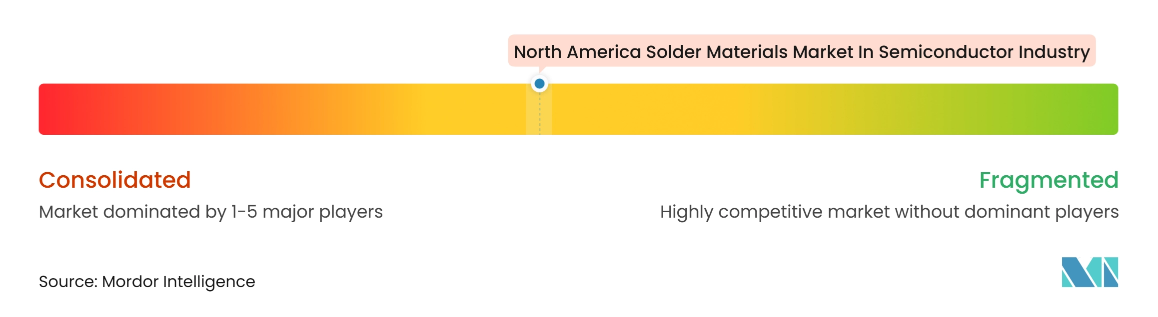
The North America solder materials market in semiconductor industry is moderately consolidated among suppliers with broad alloy portfolios, in-house flux chemistry, and established qualification data. Regional and application-specific specialists compete through fine-powder capability, microball production, and cost-focused alloys. Competition is strongest in Type 6 to Type 8 powders and sub-100 μm balls used in chiplet and wafer-level packaging. These formats require controlled atomization, narrow particle distributions, and low-alpha performance. The same requirements limit the number of suppliers that can credibly serve high-reliability applications. Sintered silver and copper pastes also compete in high-temperature power-module die attach. That pressure encourages conventional solder suppliers to add sintering products or reinforce preform offerings.
The market is shifting from formulation-only competition to a combination of material supply and process support. Application engineering, failure analysis, and recycling services can improve customer retention during multi-year qualification periods. Compliance with IPC J-STD-001 and automotive quality requirements raises the entry barrier for unqualified suppliers. In February 2025, Heraeus Electronics, MacDermid Alpha Electronics Solutions, and Henkel concluded German litigation concerning Innolot alloy technology against Senju Group. The outcome illustrates the importance of intellectual property in premium, lead-free alloy development. Suppliers are also offering lower-silver, bismuth-free, halogen-free, and ultra-fine-powder materials to address cost, process, and reliability needs.
Company product launches show how suppliers are responding to specific packaging issues. In September 2026, Indium Corporation introduced Indium12.9HF, a no-clean, halogen-free solder paste for ultra-fine-feature printing. In June 2026, MacDermid Alpha Electronics Solutions launched ALPHA OM-377 for ultra-fine feature printing in high-volume production. MacDermid Alpha also presented expanded sintering and reinforced preform offerings for power-module reliability in June 2026. Recycled-tin and halogen-free formulations are becoming part of product strategy alongside thermal and electrical performance. The North America solder materials market in semiconductor industry remains open to specialists, but larger platforms have an advantage where customers need coordinated validation across multiple assembly stages.
Leaders of North America Solder Materials Market In Semiconductor Industry
-
MacDermid Alpha Electronics Solutions
-
Indium Corporation
-
Senju Metal Industry Co., Ltd.
-
AIM Solder
-
Henkel AG and Co. KGaA
- *Disclaimer: Major Players sorted in no particular order
North America Solder Materials Market In Semiconductor Industry Companies Covered in this Report
- AIM Solder
- Alpha Assembly Solutions, MacDermid Alpha Electronics Solutions
- Ames Goldsmith Corporation
- Balver Zinn GmbH and Co. KG
- DUKSAN Hi-Metal Co., Ltd.
- FCT Solder
- Harima Chemicals Group, Inc.
- Heraeus Electronics
- Henkel AG and Co. KGaA
- Indium Corporation
- Illinois Tool Works Inc., Kester
- KOKI Company Limited
- MacDermid Alpha Electronics Solutions
- Materion Corporation
- MK Electron Co., Ltd.
- Nihon Superior Co., Ltd.
- Qualitek International, Inc.
- Senju Metal Industry Co., Ltd.
- Shenmao Technology Inc.
- Tamura Corporation
- TANAKA Holdings Co., Ltd.
Recent Industry Developments in North America Solder Materials Market In Semiconductor Industry
- October 2026: GlobalFoundries was selected as technology provider for 2 new 300 mm semiconductor fabs at its Malta, New York, site under a U.S.-Japan initiative providing up to USD 21 billion in funding. GF simultaneously reallocated USD 955 million of its existing CHIPS Act award toward advanced packaging, silicon photonics, and silicon-germanium at its New York and Vermont facilities. The project is expected to create 27,000 construction and ecosystem jobs, directly anchoring downstream demand for solder materials in domestic advanced-packaging programs.
- October 2026: Indium Corporation announced the launch of Indium12.9HF, a no-clean, halogen-free solder paste engineered for ultra-fine-feature printing to 01005 and 008004 component sizes. The formulation offers high oxidation resistance and low voiding at BGA, CSP, LGA, and QFN pad sizes as small as 175 μm, targeting advanced semiconductor packaging customers demanding finer-pitch interconnect materials.
- September 2026: Indium Corporation presented its DFLT bismuth-free, indium-containing low-temperature solder at IMAPS Symposium 2026, targeting large BGA assemblies in AI server and high-performance computing applications. The dual-powder system achieves peak reflow temperatures as low as 210°C while delivering drop-shock and electromigration performance comparable to or exceeding SAC305, addressing warpage challenges critical to next-generation AI chip packaging.
- June 2026: MacDermid Alpha Electronics Solutions launched ALPHA OM-377, a no-clean, halogen-free solder paste designed for ultra-fine feature printing to 008004 component sizes in high-volume production. The product seeks to reduce head-in-pillow and non-wet open defects to support first-pass yield improvement in densely integrated electronics assemblies.
Scope of Report on North America Solder Materials Market In Semiconductor Industry
The North America Solder Materials Market in Semiconductor Industry Market encompasses the production and supply of specialized solder materials used in semiconductor assembly, packaging, and interconnection processes. These materials enable reliable electrical connections, thermal management, and mechanical bonding between semiconductor dies, substrates, and electronic components. The market covers solder-based solutions supporting advanced packaging technologies, high-density interconnections, and miniaturized semiconductor devices. Growing demand for high-performance chips, increasing semiconductor packaging complexity, and advancements in electronic manufacturing technologies drive the adoption of solder materials across the global semiconductor industry.
The North America Solder Materials Market in Semiconductor Industry Report is Segmented by Applicable Market (Logic ICs, Memory ICs, Compound Semiconductors and Power Devices, Analog ICs, Sensors, MEMS and RF Devices, and Optical and Photonic Devices), Product Form (Solder Paste, Solder Balls and Spheres, Solder Preforms, Solder Wire, Solder Fluxes, Standalone, and Solder Powder, Externally Sold), Application and Process Step(Wafer-Level Bump Formation, Die-to-Substrate Interconnection, Conventional Flip-Chip, Package-to-Board Interconnection, BGA and CSP Ball Attach, Backside Die Attach, and Package Sealing and Component Attachment), and Geography (United States, Canada, and Mexico). The Market Forecasts are Provided in Terms of Value (USD). The Market Forecasts are Provided in Terms of Value (USD).
Segmentation Overview
| Logic ICs |
| Memory ICs |
| Compound Semiconductors and Power Devices |
| Analog ICs |
| Sensors, MEMS and RF Devices |
| Optical and Photonic Devices |
| Solder Paste |
| Solder Balls and Spheres |
| Solder Preforms |
| Solder Wire |
| Solder Fluxes, Standalone |
| Solder Powder, Externally Sold |
| Wafer-Level Bump Formation |
| Die-to-Substrate Interconnection, Conventional Flip-Chip |
| Package-to-Board Interconnection, BGA and CSP Ball Attach |
| Backside Die Attach |
| Package Sealing and Component Attachment |
| United States |
| Canada |
| Mexico |
| By Applicable Market | Logic ICs |
| Memory ICs | |
| Compound Semiconductors and Power Devices | |
| Analog ICs | |
| Sensors, MEMS and RF Devices | |
| Optical and Photonic Devices | |
| By Product Form | Solder Paste |
| Solder Balls and Spheres | |
| Solder Preforms | |
| Solder Wire | |
| Solder Fluxes, Standalone | |
| Solder Powder, Externally Sold | |
| By Application and Process Step | Wafer-Level Bump Formation |
| Die-to-Substrate Interconnection, Conventional Flip-Chip | |
| Package-to-Board Interconnection, BGA and CSP Ball Attach | |
| Backside Die Attach | |
| Package Sealing and Component Attachment | |
| By Geography | United States |
| Canada | |
| Mexico |
Key Questions Answered in the Report
What is the size of the North America solder materials market in semiconductor industry?
The market is projected to expand from USD 160.11 million in 2026 to USD 239.23 million by 2032, at a 6.75% CAGR from 2027 to 2032.
Which semiconductor category leads demand for solder materials in North America?
Logic ICs lead with a 37.11% share in 2026 and are projected to advance at a 7.11% CAGR through 2032.
Which solder material form is expected to expand the fastest?
Solder preforms are expected to expand at a 7.23% CAGR through 2032, supported by power semiconductor packaging needs.
Why is wafer-level bumping important for solder material suppliers?
Wafer-level bump formation held 28.66% of market value in 2026 and is projected to advance at a 7.42% CAGR through 2032.
Which country is expected to record the fastest regional expansion?
Mexico is projected to record a 7.33% CAGR through 2032, supported by regional assembly, testing, and packaging activity.
What factors can limit demand for solder materials in semiconductor packaging?
Metal-price volatility, lead-free qualification requirements, fine-pitch reliability risks, and substitution by copper pillars, hybrid bonding, and sintered materials can limit demand.