
North America IC Design Services Market Size and Share
Market Overview
| Study Period | 2021 - 2032 |
|---|---|
| Forecast Data Period | 2027 - 2032 |
| Base Year Market Size (2026) | USD 4.66 Billion |
| Market Size (2027) | USD 5.75 Billion |
| Market Size (2032) | USD 8.95 Billion |
| Growth Rate (2027 - 2032) | 9.25 % |
| Market Concentration | Low |
Major Players *Disclaimer: Major Players sorted in no particular order Image © Mordor Intelligence. Reuse requires attribution under CC BY 4.0. | |
North America IC Design Services Market Analysis by Mordor Intelligence
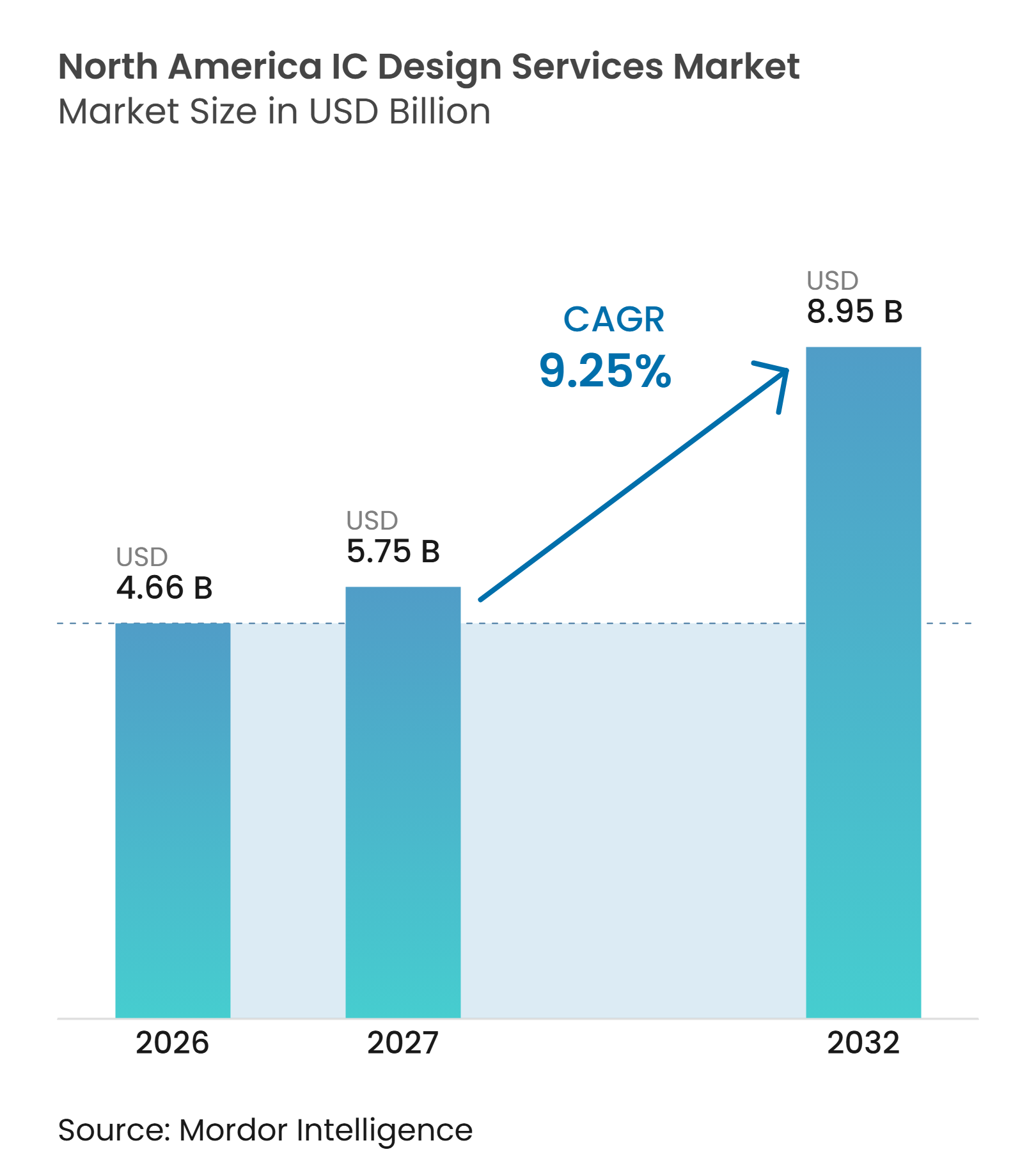
The North America IC design services market size is projected to expand from USD 4.66 billion in 2026 and USD 5.75 billion in 2027 to USD 8.95 billion by 2032, registering a CAGR of 9.25% between 2027 and 2032. The North America IC design services market is being shaped by customers that need purpose-built silicon for artificial intelligence workloads, automotive electronics, and defense systems. New domestic fabrication capacity is increasing the need for design programs that can use those facilities effectively. Large customers are placing more value on partners that can combine architecture, verification, physical design, packaging coordination, and production support. The North America IC design services market also faces pressure from a limited supply of experienced engineers and higher costs for advanced design tools. These conditions favor providers with established foundry relationships, experienced technical teams, and secure design workflows.
Key Report Takeaways
-
By service type, Digital IC Design Services held 29.13% of the regional IC design services market share in 2026, while Design Verification Services is projected to expand at a 10.64% CAGR through 2032.
-
By end-user application, AI, HPC, and Data Centers accounted for 32.84% of the regional IC design services market size in 2026 and were also the fastest-growing applications.
-
By design complexity, Mature Nodes (8nm-28nm) held a 43.27% share in 2026, while Advanced Nodes (≤7nm) are projected to expand at a 9.86% CAGR through 2032.
-
By geography, the United States held an 81.42% share in 2026, while Mexico is projected to expand at a 9.91% CAGR through 2032.
Note: Market numbers in this report are based on Mordor Intelligence's proprietary estimation framework, which combines nine months of actuals with Q4 projections for base year 2026.
Market Trends and Insights
Drivers Impact Analysis of North America IC Design Services Market*
| Driver | (~) % Impact on CAGR Forecast | Geographic Relevance | Impact Timeline |
|---|---|---|---|
| Domestic Semiconductor Manufacturing Expansion and CHIPS Act Incentives | +2.5% | United States, with spillover to Canada and Mexico | Long term (≥ 4 years) |
| AI Accelerators and Custom ASIC Adoption by Hyperscalers | +2.1% | United States core, with global customer demand flows | Short term (≤ 2 years) |
| Outsourcing of Semiconductor Engineering Services | +1.3% | United States and Canada | Medium term (2-4 years) |
| Rising Semiconductor Content in Automotive Applications | +0.9% | United States and Mexico, with spillover to Canada | Medium term (2-4 years) |
| Defense Modernization and Secure Semiconductor Architectures | +0.6% | United States | Short term (≤ 2 years) |
| Chiplet Architectures and Advanced Packaging Adoption | +0.5% | United States core and North America broadly | Long term (≥ 4 years) |
| Source: Mordor Intelligence | |||
Domestic Semiconductor Manufacturing Expansion and CHIPS Act Incentives
The North America IC design services market is benefiting from semiconductor capacity projects supported by the CHIPS and Science Act framework. Investments by TSMC, Intel, and Samsung in Arizona, Ohio, Oregon, and Texas create a larger domestic base for chip programs and design support. Each advanced fabrication site needs a pipeline of customer designs to use capacity efficiently, which creates demand before wafer production reaches full scale. Natcast introduced a design enablement gateway and silicon aggregation service that can help early-stage companies access advanced-node tape-out capacity. California's DREAMS initiative also deployed Synopsys Cloud, which offers unlimited software licensing for defense-adjacent programs, improving access to qualified design tools. The CHIPS Program Office's shift to portfolio management in 2026 increases the importance of compliance and delivery performance for firms serving funded recipients.
AI Accelerators and Custom ASIC Adoption by Hyperscalers
Hyperscalers are moving toward internally specified AI silicon, which is changing the type of work requested from the North America IC design services market. These programs need close coordination across logic design, verification, physical implementation, packaging, and manufacturing. OpenAI and Broadcom developed the Jalapeño inference accelerator from design through manufacturing tape-out in 9 months, using AI models to accelerate optimization. That delivery period raises customer expectations for firms whose conventional programs can take 18 to 24 months. Providers with AI-supported electronic design automation workflows and dedicated customer engineering teams are better placed to respond. This work also creates durable engagements because accelerator programs require ongoing design changes, validation, and production coordination.
Outsourcing Of Semiconductor Engineering Services
The North America IC design services market is supported by clients that need specialist engineering capacity faster than internal hiring can provide. Fabless companies and integrated device manufacturers can outsource physical design, verification, and IP integration while keeping architecture and differentiated intellectual property in-house. This model is useful when several programs must advance simultaneously. L&T Technology Services signed a USD 100 million multiyear agreement in September 2025 with a US-based industrial equipment manufacturer serving the semiconductor value chain.[1] The agreement covered new product development, sustenance engineering, value engineering, and platform automation. The contract supports the case for full-cycle partners rather than narrow point-service providers.
Rising Semiconductor Content In Automotive Applications
Automotive electrification and software-defined vehicle programs are expanding the range of semiconductor design work required by vehicle manufacturers and their suppliers. Electric vehicles need power management ICs, battery management chips, and traction inverter controllers. Software-defined vehicles also require radar system-on-chips, centralized domain controllers, and processors capable of supporting advanced driver assistance functions. HCLTech supported a global automotive semiconductor company with a radar system-on-chip program from RTL design through physical implementation and ISO 26262 functional safety sign-off. ASICLAND also signed a June 2025 agreement with a US integrated device manufacturer to target automotive semiconductor demand. The North America IC design services industry benefits as vehicle programs move toward more complex designs at 5nm and below.
Restraints Impact Analysis of North America IC Design Services Market*
| Restraint | (~) Impact on CAGR Forecast | Geographic Relevance | Impact Timeline |
|---|---|---|---|
| High Engineering Labor Costs and Talent Competition | -1.3% | United States, extending to Canada | Long term (≥ 4 years) |
| High EDA Licensing Costs and Advanced Node Complexity | -0.9% | United States core and broader North America | Medium term (2-4 years) |
| Export Controls and Cross-Border Technology Restrictions | -0.6% | United States, with spillover to Canada and Mexico | Short term (≤ 2 years) |
| Shortage of Specialized Semiconductor Design Engineers | -0.5% | United States and Canada | Long term (≥ 4 years) |
| Source: Mordor Intelligence | |||
High Engineering Labor Costs And Talent Competition
The supply of experienced semiconductor engineers remains a constraint on the North America IC design services market. Experienced verification, physical design, and analog engineers are costly, especially for advanced-node programs. Design service providers must meet shorter delivery schedules while managing higher compensation costs. This can reduce margins when customers seek fixed-price or tightly scoped work. It also creates direct competition between service firms and their own clients for the same engineering talent. Synopsys identifies the shortage of skilled semiconductor engineers as a continuing challenge for design organizations and points to training and workforce development approaches as part of the response.
High EDA Licensing Costs And Advanced Node Complexity
Advanced-node work requires qualified electronic design automation tools, process design kits, and specialized technical expertise. These requirements can make it difficult for mid-sized providers to compete for leading-edge programs. Costs rise further when projects need AI-assisted physical implementation tools and larger verification environments. The resulting expense favors firms that can spread tool investments across several large customer programs. Smaller providers may instead focus on analog, mixed-signal, mature-node, or vertical-specific work. The North America IC design services market therefore has a practical barrier between firms that can deliver turnkey advanced-node projects and firms that specialize in narrower services.
*Our forecasts treat driver/restraint impacts as directional, not additive. The impact forecasts reflect baseline growth, mix effects, and variable interactions.
North America IC Design Services Market Segment Analysis
By Service Type:
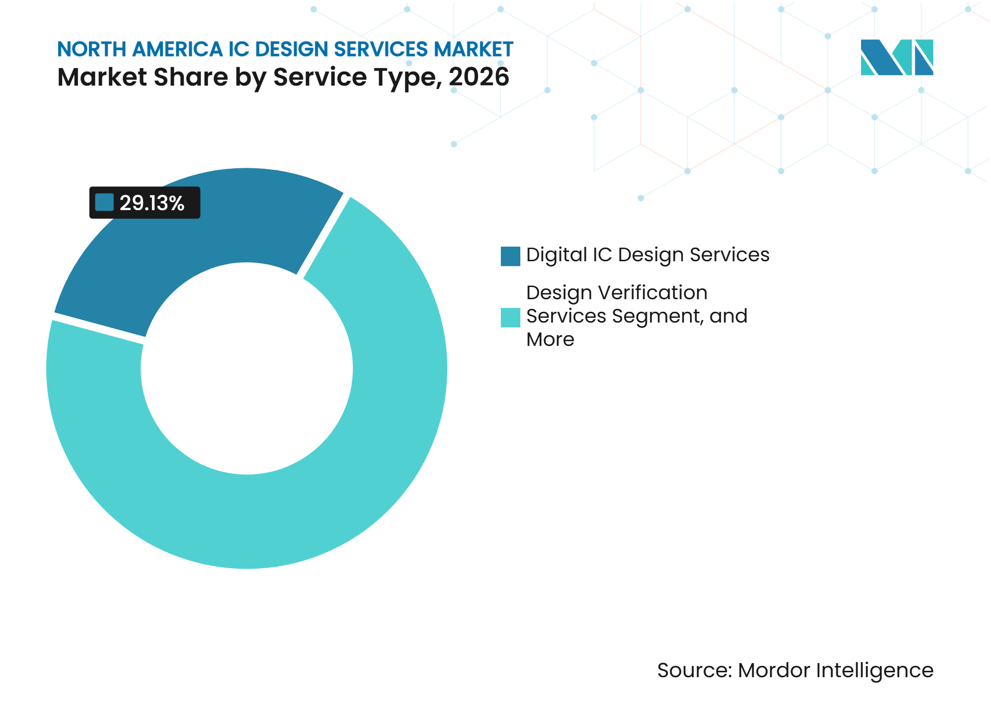
Verification Demand Outpaces Traditional Design SegmentsDigital IC Design Services held 29.13% of the North America IC design services market share in 2026. The segment is supported by the region's concentration of fabless system-on-chip and processor developers. These customers need RTL design teams that can work with advanced electronic design automation flows. Digital design also remains central to processor, networking, and accelerator programs with large transistor counts. Physical design and layout providers contribute to chiplet integration and advanced packaging programs. IP development and design support help customers reuse validated subsystems across multiple products.
Design Verification Services is projected to expand at a 10.64% CAGR through 2032. Verification has become more important because design errors at leading-edge nodes can require an expensive silicon re-spin. The work includes functional coverage, simulation, and testing of edge cases before tape-out. Its value increases even when RTL headcount is stable because validation requirements increase with design complexity. Analog mixed-signal services remain important for automotive, industrial, power management, and medical applications. ISO 26262 and IEC 60601 requirements can raise the value of teams with proven domain experience.



By End-User Application:
AI And HPC Set The Trajectory For The Broader MarketAI, HPC, and Data Centers accounted for 32.84% of the North America IC design services market size in 2026. Custom AI accelerator programs require work across architecture, implementation, packaging, and foundry coordination. These projects commonly extend from architecture definition to production tape-out over 2 to 3 years. Their duration gives service providers more stable work than short consumer-electronics design contracts. The need for high bandwidth, power efficiency, and specialized compute also raises the technical requirements for each program. This application is both the largest and fastest-growing end-user segment in the supplied data.
Automotive is the next major demand area, as it requires radar system-on-chips, battery-management chips, and domain-controller ASICs. ISO 26262 functional safety requirements make complete design and validation capability important in automotive programs. Consumer electronics work is increasingly focused on differentiated premium devices such as smartwear, AR/VR silicon, and edge AI processors. Industrial, telecom, and networking customers continue to require power-efficient and thermally robust integrated circuits at mature nodes. Defense and aerospace programs can command premium pricing because they need domestic traceability under the DMEA framework. Medical and healthcare customers favor teams with analog capability and experience with FDA-compliant design workflows.
By Design Complexity:
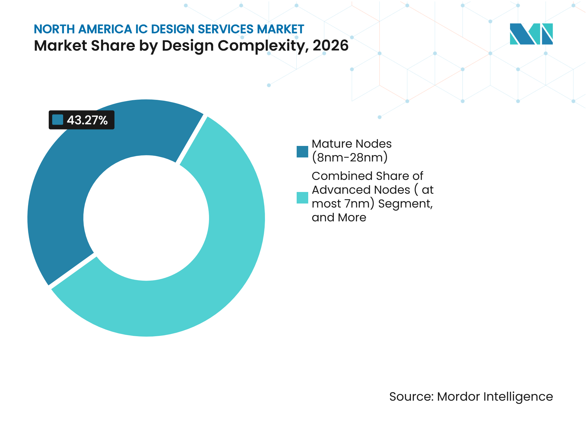
Advanced Nodes Redefine Design Cost EconomicsMature Nodes (8nm-28nm) held 43.27% of the North America IC design services market share in 2026. Automotive, industrial, medical, and legacy wireless applications continue to use these process technologies. Mature processes offer higher yield predictability and lower design risk than leading-edge nodes. This supports more consistent delivery schedules for design service engagements. These nodes also remain suitable for products where cost, availability, and long qualification cycles matter more than maximum density. Their relevance preserves work for firms with expertise outside the most advanced process generations.
Advanced Nodes (≤7nm) are projected to expand at a 9.86% CAGR through 2032. AI accelerators, high-performance computing, and high-bandwidth networking programs need the density and energy efficiency these nodes can provide. CSIS reported that developing a leading-edge 2nm chip costs 2.4 times as much as developing a 7nm design. This cost narrows the pool of service providers capable of funding the required engineering, tools, and design infrastructure. Legacy Nodes (>28nm) still serve cost-sensitive IoT, analog sensor, and power-management products where supply continuity is important. Foundry ecosystem qualifications from TSMC, Samsung, and Intel Foundry can add an additional barrier to entry through tool qualification and process design kit sign-off.

Geography Analysis
United States
The United States held 81.42% of the regional IC design services market share in 2026. Silicon Valley, Austin, San Diego, and the Research Triangle are home to dense clusters of fabless companies, cloud operators, electronic design automation vendors, and defense electronics programs. The CHIPS Program Office's 2026 shift to portfolio management has strengthened the focus on delivery and compliance among organizations supporting funded projects. TSMC's Arizona operations, Intel facilities in Ohio and Oregon, and Samsung's Texas complex create a broader domestic base for design engagements. High-assurance automotive and defense work favors providers that can demonstrate ISO 26262, DO-254, or DMEA Trusted IC-compliant workflows. ForwardEdge ASIC received DMEA Trusted IC vendor accreditation in February 2026, confirming 100% domestically traceable ASIC and FPGA design capability. Natcast's design enablement gateway can also widen access to advanced-node tape-out for new chip companies
Mexico
Mexico is projected to expand at a 9.91% CAGR through 2032 within the North America IC design services market. Its role is supported by North American supply chain integration under the USMCA and related semiconductor initiatives. The Secretariat of Science, Humanities, Technology and Innovation launched the Kutsari Project in February 2025, including a National Center for Semiconductor Design in Jalisco, Puebla, and Sonora. The program targets designs for automotive, household appliance, and medical device applications by 2027.[2] Intel, Infineon, Skyworks Solutions, and Texas Instruments have manufacturing operations in Mexico, creating an anchor base for future local design demand. Engineering talent remains a structural constraint even though TecNM semiconductor diploma programs enrolled more than 5,000 students in an English-for-semiconductors course. The local supply of qualified IC design engineers must deepen for the country to sustain rapid scaling.
Canada And Regional Integration
Canada contributes specialized capability in photonics IC design, quantum hardware research, and AI chip architecture. The North America IC design services market can draw on these specialist areas as customer requirements widen. CMC Microsystems and the University of Toronto support design prototyping and links between academic research and industrial users. The Wilson Center described a “Designed in North America” approach that links Canadian engineering capabilities with U.S. and Mexican assets. This regional structure can help companies coordinate design, fabrication, assembly, testing, and packaging across North America. Canada's relatively lower engineering costs compared with major U.S. hubs can support nearshore verification and physical-design capacity. The regional IC design services market size is supported by this distribution of engineering and manufacturing capabilities across the region. Photonics and quantum design niches offer areas for differentiation, although their commercial scale is expected to develop over a longer period. The regional model depends on practical workforce coordination, secure data handling, and compatible supply-chain rules.
Competitive Landscape
Market Concentration
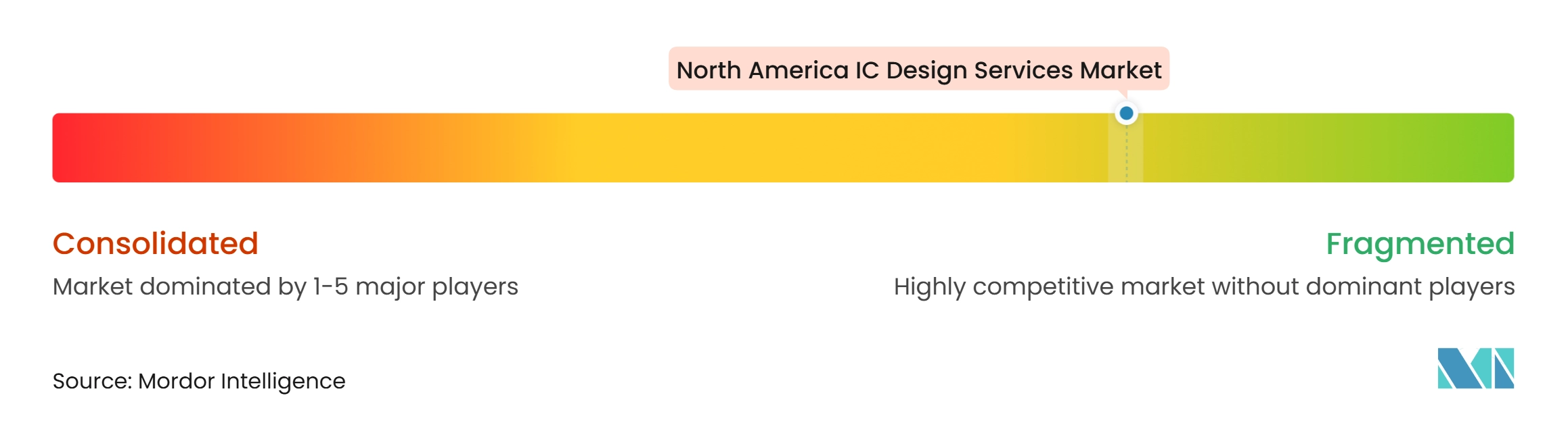
The North America IC design services market is fragmented, with a mix of tier-2 and tier-3 providers. The North America IC design services market rewards providers that can combine technical depth with dependable delivery. Taiwan-based companies including Global Unichip, Alchip Technologies, and Faraday Technology hold leading positions in turnkey advanced-node work. Their strength comes from close relationships with foundries and experience with complex AI chip programs. Indian engineering services providers such as HCLTech, L&T Technology Services, eInfochips, and Tessolve compete for mid-market work with full-cycle engineering teams. Tessolve reports that it deploys 1,250 IC design engineers across nodes from 2nm to 180nm. Competition increasingly depends on the ability to integrate design, verification, packaging, and manufacturing support into a single delivery model.
Secure domestic design is a clear area of competition in defense applications. Arteris, BAE Systems, and SiFive received an additional USD 3.3 million in October 2026 through the Trusted and Assured Microelectronics program to develop repeatable security-assurance methods for third-party silicon IP. The program raises the evidence and traceability requirements for companies serving defense system-on-chip work. eInfochips demonstrated an end-to-end turnkey ASIC flow in October 2026, covering design, fabrication, packaging, and silicon bring-up.[3] It also joined the Samsung Advanced Foundry Ecosystem as a Virtual Design Partner in February 2025. These moves show how foundry access and complete delivery capability are becoming practical differentiators.
Opportunities remain in traceable defense designs, analog and mixed-signal work for vehicle electrification, and chiplet support for customers moving from monolithic designs to multi-die systems. SEMIFIVE's cumulative Q3 2025 order intake exceeded KRW 125.7 billion (USD 87.1 million), above its full-year 2024 total. The company later signed a KRW 18 billion (USD 12.5 million) AI NPU turnkey design contract in March 2026 for Samsung Foundry's 4nm SF4X process. Socionext introduced RTL-configurable Flexlets in October 2025 for UCIe, UALink, PCIe Gen7, and 2.5D/3D packaging across 5nm to 2nm nodes. Firms that can use AI-assisted design flows may shorten tape-out cycles, but they must also manage higher tool and engineering costs. Providers without comparable technical depth may remain focused on mature-node or specialist applications.
North America IC Design Services Industry Leaders
-
Alchip Technologies, Ltd.
-
Global Unichip Corp. (GUC)
-
eInfochips (an Arrow Electronics company)
-
HCL Technologies Limited
-
Cadence Design Systems, Inc.
- *Disclaimer: Major Players sorted in no particular order
North America IC Design Services Market Companies Covered in this Report
- Global Unichip Corporation
- Alchip Technologies Limited
- Faraday Technology Corporation
- VeriSilicon Microelectronics (Shanghai) Co., Ltd.
- SEMIFIVE Co., Ltd.
- CoAsia SEMI Co., Ltd.
- Sondrel Limited
- EnSilica plc
- Racyics GmbH
- ICsense NV
- E-Infochips Private Limited
- HCL Technologies Limited
- L&T Technology Services Limited
- MosChip Technologies Limited
- Tessolve Semiconductor Private Limited
- Cadence Design Systems, Inc.
- Capgemini SE
- Wipro Limited
- Tata Elxsi Limited
- Cyient Limited
- ACL Digital Private Limited
Recent Industry Developments in North America IC Design Services Market
- October 2026: eInfochips, an Arrow Electronics company, demonstrated end-to-end turnkey ASIC design capability through the development, fabrication, packaging, and silicon bring-up of a test chip at its San Jose facility, reinforcing its role as a full-lifecycle custom-silicon provider for automotive, industrial, and semiconductor programs.
- October 2026: Arteris, in collaboration with BAE Systems and SiFive, received an additional USD 3.3 million in funding through the US Department of Defense's Trusted and Assured Microelectronics (T&AM) program to develop repeatable, evidence-based methodologies for verifying the secure integration of third-party silicon IP into mission-critical SoC designs.
- August 2026: L&T Technology Services (LTTS) secured a five-year, USD 75 million engagement from a leading global technology enterprise for end-to-end product engineering, software development, testing, validation, and sustenance engineering, with a dedicated Engineering Center to be established for the client's digital functions.
- March 2026: SEMIFIVE signed a KRW 18 billion (USD 12.5 million) AI NPU turnkey design contract with an AI semiconductor fabless company, covering a high-performance neural processing unit on Samsung Foundry's advanced 4nm SF4X process. The contract is a follow-on program with the same client, reflecting SEMIFIVE's growing position as a specialized AI chip design house serving advanced-node compute programs.
North America IC Design Services Market Report Scope
The North America IC Design Services Market comprises revenue generated by companies providing outsourced and specialized integrated circuit (IC) design and engineering services to semiconductor companies, fabless firms, integrated device manufacturers (IDMs), OEMs, and other technology developers. The market encompasses the design and development of analog, digital, and analog mixed-signal (AMS) integrated circuits, as well as physical design and layout, design verification, IP development, and associated design support services.
The North America IC Design Services Market Report is Segmented by Service Type (Analog IC Design Services, Digital IC Design Services, Analog Mixed-Signal (AMS) IC Design Services, Physical Design and Layout Services, Design Verification Services, IP Development and Design Support Services, and Other Service Types), End-User Application (Automotive, AI, HPC, and Data Centers, Consumer Electronics, Industrial, Defense and Aerospace, Medical and Healthcare, Telecom and Networking, and Other End-User Applications), Design Complexity (Advanced Nodes (≤7nm), Mature Nodes (8nm–28nm), and Legacy Nodes (Above 28nm)), and Geography (United States, Canada, and Mexico). The Market Forecasts are Provided in Terms of Value (USD).
Segmentation Overview
| Analog IC Design Services |
| Digital IC Design Services |
| Analog Mixed-Signal (AMS) IC Design Services |
| Physical Design and Layout Services |
| Design Verification Services |
| IP Development and Design Support Services |
| Other Service Types |
| Automotive |
| AI, HPC, and Data Centers |
| Consumer Electronics |
| Industrial |
| Defense and Aerospace |
| Medical and Healthcare |
| Telecom and Networking |
| Other End-User Applications |
| Advanced Nodes (≤7nm) |
| Mature Nodes (8nm–28nm) |
| Legacy Nodes (Above 28nm) |
| United States |
| Canada |
| Mexico |
| By Service Type | Analog IC Design Services |
| Digital IC Design Services | |
| Analog Mixed-Signal (AMS) IC Design Services | |
| Physical Design and Layout Services | |
| Design Verification Services | |
| IP Development and Design Support Services | |
| Other Service Types | |
| By End-User Application | Automotive |
| AI, HPC, and Data Centers | |
| Consumer Electronics | |
| Industrial | |
| Defense and Aerospace | |
| Medical and Healthcare | |
| Telecom and Networking | |
| Other End-User Applications | |
| By Design Complexity | Advanced Nodes (≤7nm) |
| Mature Nodes (8nm–28nm) | |
| Legacy Nodes (Above 28nm) | |
| By Country | United States |
| Canada | |
| Mexico |
Key Questions Answered in the Report
What is the North America IC design services market size?
The North America IC design services market size is projected to increase from USD 4.66 billion in 2026 and USD 5.75 billion in 2027 to USD 8.95 billion by 2032.
What is driving demand for IC design services in North America?
Demand is supported by custom AI accelerators, new domestic semiconductor capacity, outsourced engineering work, and rising semiconductor content in vehicles.
Which IC design service holds the largest share in North America?
Digital IC Design Services held 29.13% share in 2026, while Design Verification Services is projected to record the highest CAGR at 10.64% through 2032.
Which application uses the most IC design services?
AI, HPC and Data Centers accounted for 32.84% share in 2026 and was also the fastest-growing end-user application in the supplied data.
Why are advanced-node design programs difficult for smaller providers?
Advanced-node work requires costly qualified tools, foundry process support, complex verification, and engineering teams with proven leading-edge experience.
Which country is expanding fastest in North American IC design services?
Mexico is projected to expand at a 9.91% CAGR through 2032, supported by semiconductor ecosystem initiatives and regional supply-chain integration.