
Size and Share of Molybdenum Market For Semiconductor Materials
Market Overview
| Study Period | 2022 - 2032 |
|---|---|
| Market Size (2027) | USD 443.88 Million |
| Market Size (2032) | USD 638.14 Million |
| Growth Rate (2027 - 2032) | 7.53 % |
| Fastest Growing Market | Asia-Pacific |
| Largest Market | Asia-Pacific |
| Market Concentration | Medium |
Major Players *Disclaimer: Major Players sorted in no particular order Image © Mordor Intelligence. Reuse requires attribution under CC BY 4.0. | |
Analysis of Molybdenum Market For Semiconductor Materials by Mordor Intelligence
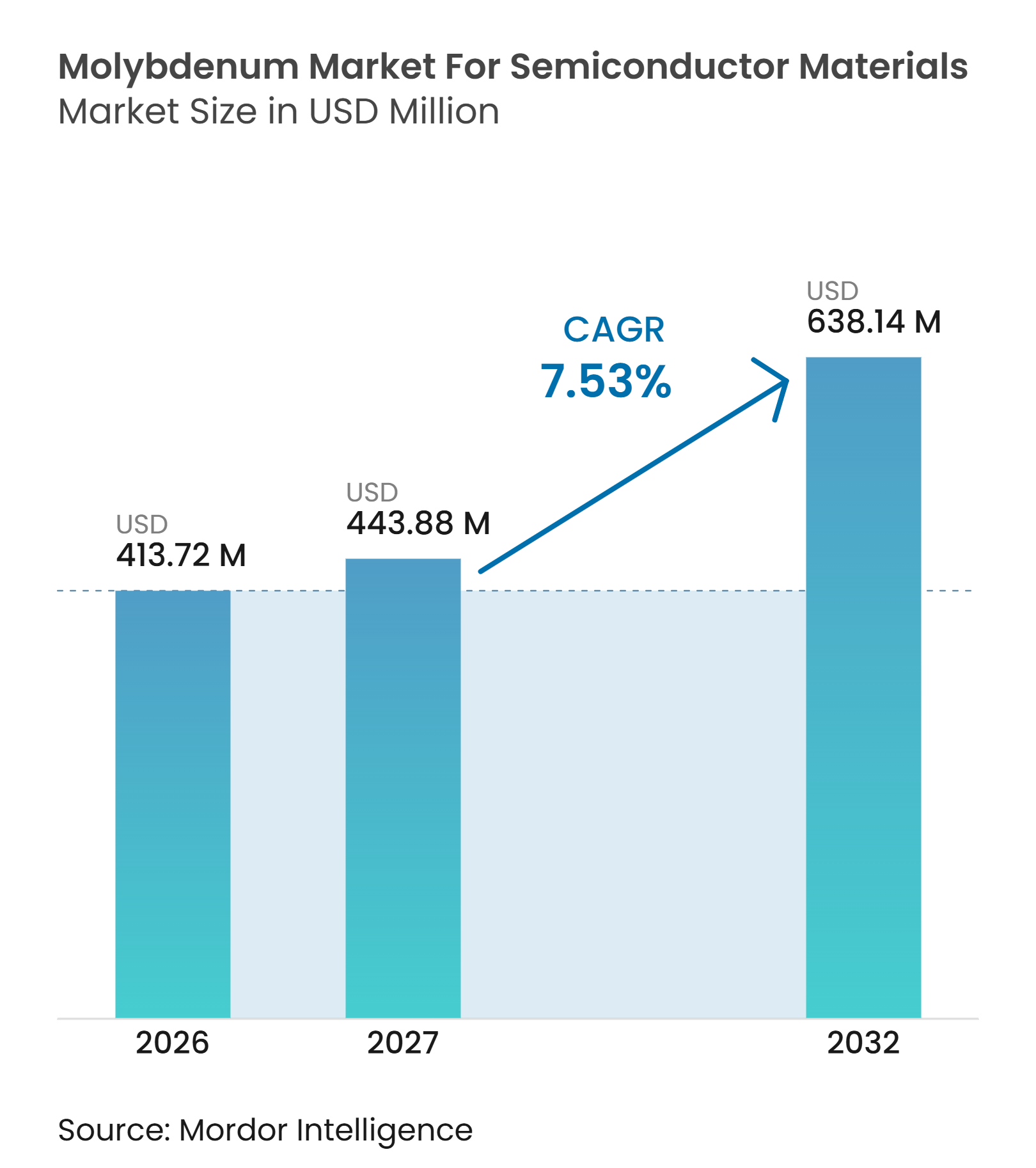
The Molybdenum Market for Semiconductor Materials Industry size was valued at USD 413.72 million in 2026 and is estimated to grow from USD 443.88 million in 2027 to reach USD 638.14 million by 2032, at a CAGR of 7.53% during the forecast period (2027-2032). The molybdenum market for semiconductor materials is supported by new leading-edge logic and memory fabrication capacity, which increases recurring use of sputtering targets and deposition precursors. Demand is also shifting toward molybdenum, where shrinking dimensions make tungsten less suitable for contacts and word lines. Higher purity requirements are raising the value of qualified material and strengthening established suppliers’ positions. Supply strategies increasingly focus on regional production and second-source qualification because export licensing and customer approval requirements can limit material availability. The molybdenum market for semiconductor materials also gains a separate demand channel from advanced packaging, where chiplets, fan-out packaging, and 3D integration require materials for redistribution layers and thermal management.
Key Report Takeaways
- By product type, molybdenum sputtering targets held 52.11% of the molybdenum market for semiconductor materials share in 2026, while molybdenum compounds and precursors are forecast to advance at an 8.12% CAGR through 2032.
- By application, wafer fabrication held 38.53% of the molybdenum market for semiconductor materials share in 2026, while semiconductor packaging is forecast to advance at an 8.34% CAGR through 2032.
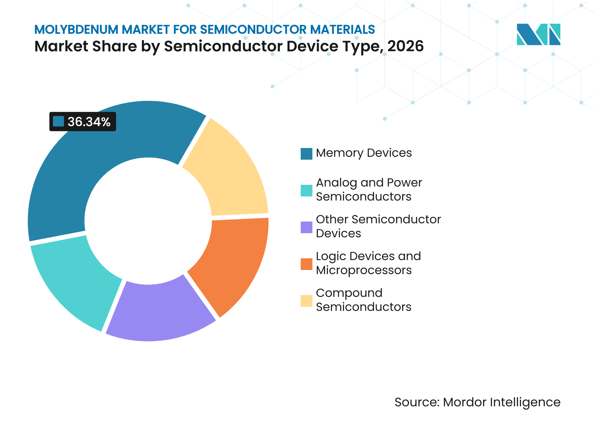
- By semiconductor device type, memory devices held 36.34% of the molybdenum market for semiconductor materials share in 2026 and are forecast to advance at an 8.68% CAGR through 2032.
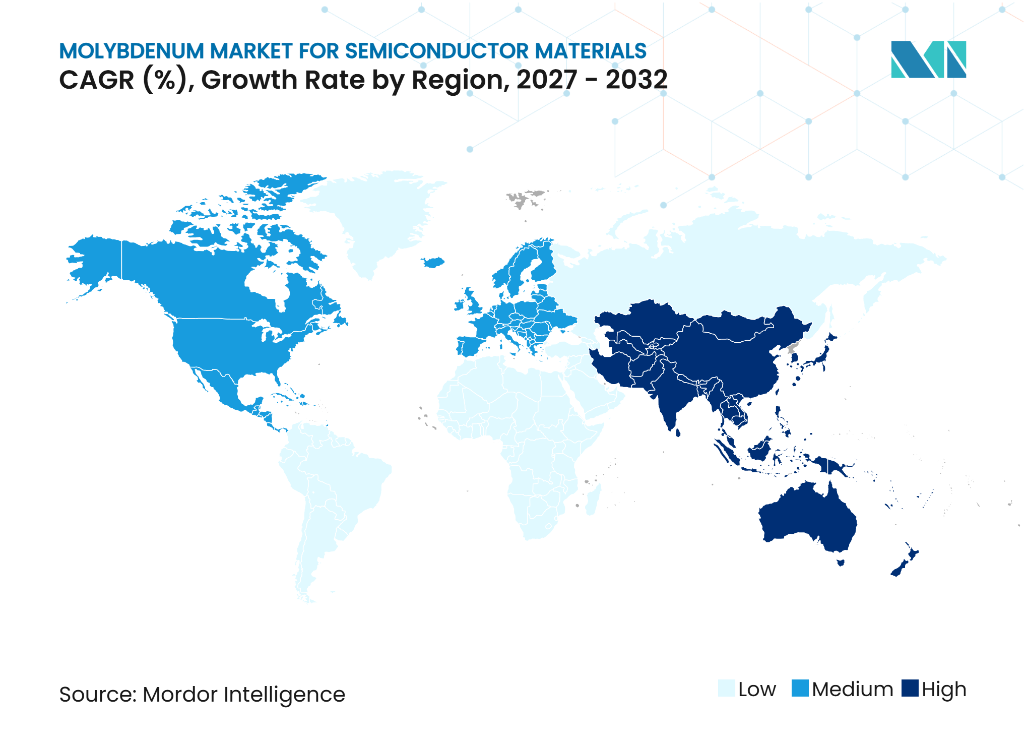
- By geography, Asia-Pacific held 54.67% of the molybdenum market for semiconductor materials share in 2026 and is forecast to advance at an 8.55% CAGR through 2032.
Note: Market numbers in this report are based on Mordor Intelligence's proprietary estimation framework, which combines nine months of actuals with Q4 projections for base year 2026.
Market Trends and Insights
Drivers Impact Analysis of Molybdenum Market For Semiconductor Materials*
| Driver | (~) % Impact on CAGR Forecast | Geographic Relevance | Impact Timeline |
|---|---|---|---|
| Advanced Logic and Memory-Fab Expansion | +2.8% | Global, led by APAC and North America | Short term (≤ 2 years) |
| Transition from Tungsten to Molybdenum in Scaled Contacts and Wordlines | +2.3% | APAC core (Taiwan, South Korea, Japan), North America | Medium term (2-4 years) |
| Rising Purity and Particle-Control Requirements in Semiconductor PVD | +0.9% | Global | Short term (≤ 2 years) |
| Qualification-Led Demand for Regional and Multi-Sourced Target Supply | +0.7% | North America and EU, spillover to APAC | Medium term (2-4 years) |
| Molybdenum Consumption Increase from Barrierless Metallization and Backside Power Research | +0.5% | APAC core, North America | Long term (≥ 4 years) |
| Source: Mordor Intelligence | |||
Advanced Logic and Memory-Fab Expansion
The molybdenum market for semiconductor materials benefits from a large expansion in logic and memory manufacturing capacity. The Semiconductor Industry Association projected that U.S. chipmaking capacity would grow 203% between 2022 and 2032, the highest projected rate globally. Each new 300 mm fab line requires recurring deposition materials, including molybdenum targets, powder, and thin-film precursors. Target replacement is linked to deposition hours, which gives established producers a recurring source of demand after a fab enters production. The European Chips Act also supported public and private investment across the semiconductor value chain, sustaining demand for equipment and specialty materials. In Japan, the Ministry of Economy, Trade and Industry approved JX Advanced Metals Corporation’s supply assurance plan in July 2025 with maximum support of JPY 2.2 billion (approximately USD 14.7 million) in investment, under the Economic Security Promotion Act[1].
Transition from Tungsten to Molybdenum in Scaled Contacts and Wordlines
The molybdenum market for semiconductor materials gains momentum as chipmakers assess alternatives to tungsten at smaller geometries. Molybdenum has a bulk resistivity of 5.34 μΩ·cm, compared with 5.6 μΩ·cm for tungsten, and this difference becomes more important as surface and grain-boundary effects increase at nanoscale dimensions. Kioxia reported that a molybdenum word-line approach reduced pitch by 7.3% while maintaining resistance-capacitance (RC) performance and increased bit density by 16.3%. This substitution supports demand for sputtering targets used in physical vapor deposition and precursors used in chemical vapor deposition and atomic layer deposition. JX Advanced Metals Corporation completed the mass-production ramp of a 6N-purity molybdenum dioxide dichloride line at its Ibaraki Office in March 2026. The fluorine-free precursor route can also address reliability concerns associated with tungsten hexafluoride, which makes molybdenum relevant to both performance and process integration.
Rising Purity and Particle-Control Requirements in Semiconductor PVD
The molybdenum market for semiconductor materials is shaped by strict purity and particle-control requirements at advanced nodes. Plansee SE states that its semiconductor-grade molybdenum targets meet a minimum purity of 99.995%, or 4N5. At sub-10 nm dimensions, particles and metallic contaminants can cause defects that place high-value wafer output at risk. This raises the importance of audit history, material traceability, and stable production processes in supplier selection. Materion Corporation stated in its third-quarter 2025 earnings call that demand for its atomic layer deposition molybdenum portfolio was strong because of its performance in smaller-node chips, while high-performance memory application sales rose more than 30% year to date excluding China. Semiconductor Equipment and Materials International (SEMI) material purity and particle-cleanliness expectations therefore support pricing discipline among suppliers that have already passed fab qualification.
Molybdenum Consumption Increase from Barrierless Metallization and Backside Power Research
The molybdenum market for semiconductor materials has a longer-term opportunity in barrierless metallization and backside power research. Molybdenum can reduce the need for separate barrier layers in some contact structures, which may simplify deposition sequences. Research cited by the International Molybdenum Association reported that a barrierless hybrid molybdenum scheme reduced overall contact resistance by 56% compared with a conventional copper dual-damascene design. Such designs remain dependent on process qualification and device reliability results. Their adoption would require both high-purity source materials and deposition chemistry suited to tightly controlled film properties. The opportunity is therefore linked to technical progress at leading logic and memory nodes rather than broad, immediate replacement across all semiconductor production.
Restraints Impact Analysis of Molybdenum Market For Semiconductor Materials*
| Restraint | (~) % Impact on CAGR Forecast | Geographic Relevance | Impact Timeline |
|---|---|---|---|
| High Qualification Costs and Long Customer Approval Cycles | -1.0% | Global | Medium term (2-4 years) |
| Concentration of High-Purity Feedstock and Specialized Processing Capacity | -0.9% | Global, most acute in APAC and North America | Long term (≥ 4 years) |
| Oxidation, Precursor Stability, and Film-Integration Risks at Advanced Nodes | -0.6% | APAC core, North America | Short term (≤ 2 years) |
| Source: Mordor Intelligence | |||
High Qualification Costs and Long Customer Approval Cycles
Supplier qualification limits the speed at which the molybdenum market for semiconductor materials can add new sources of supply. A leading-edge fab evaluates a new sputtering target supplier through production splits, electrical parametric testing, full reliability stress, and final approval from process integration teams. This process has typically taken 12 to 24 months. The timeframe can delay conversion of customer interest into material revenue. It can also discourage customers from switching suppliers even when an alternative offers a price or purity advantage. Incumbents retain an advantage because changes to an approved material can trigger another qualification cycle.
Concentration of High-Purity Feedstock and Specialized Processing Capacity
High-purity feedstock and specialized processing capacity remain constraints for the molybdenum market for semiconductor materials. China’s Ministry of Commerce imposed export controls in February 2025 on molybdenum alloys containing more than 97% molybdenum by weight and on related production technologies, requiring export licenses[2]. Downstream suppliers need specialized sintering, rolling, and grain-control capabilities to meet semiconductor-grade microstructure requirements. This limits the speed at which capacity can respond to a disruption or demand increase. The European Union’s Critical Raw Materials Act adds supply-chain monitoring and documentation obligations for strategic materials, affecting procurement practices for closely related refractory-metal supply chains. These conditions can increase lead-time risk and complicate supply planning for fabs.
*Our forecasts treat driver/restraint impacts as directional, not additive. The impact forecasts reflect baseline growth, mix effects, and variable interactions.
Molybdenum Market For Semiconductor Materials Segment Analysis
By Product Type:
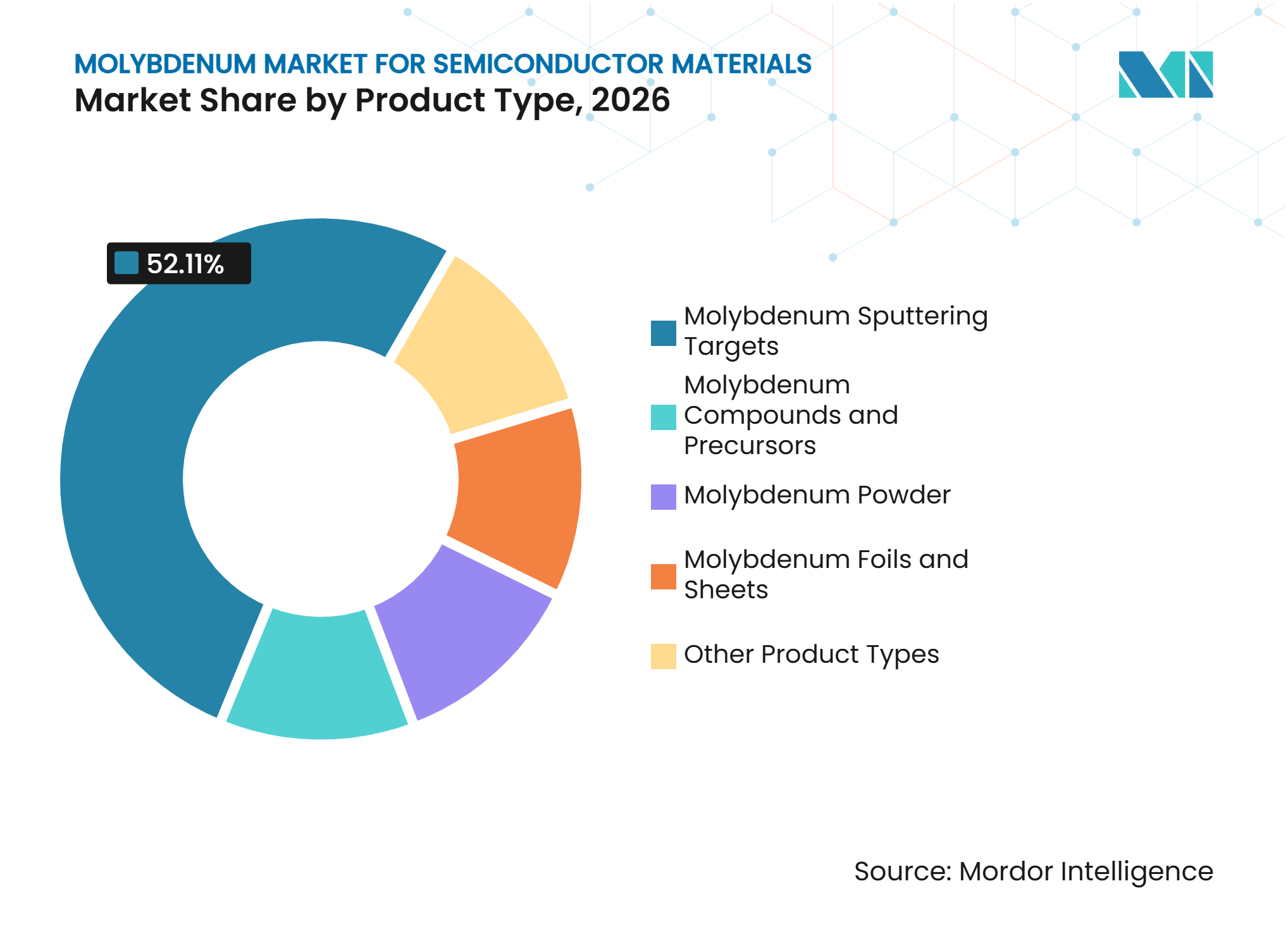
Molybdenum Sputtering Targets Lead, While Molybdenum Compounds and Precursors ExpandMolybdenum sputtering targets held 52.11% of the molybdenum market for semiconductor materials in 2026. Their position reflects the extensive use of physical vapor deposition in front-end wafer fabrication for memory and logic chips. Tighter specifications for transition-metal layers increase requirements for purity and grain control. Molybdenum powder provides feedstock for target manufacturing and ceramic metallization. Molybdenum foils and sheets support uses such as metallization in power-device packaging, while other product types serve specialized equipment and research applications.
Molybdenum compounds and precursors are projected to advance at an 8.12% CAGR through 2032. Their growth is tied to chemical vapor deposition and atomic layer deposition routes for word-line and contact applications. JX Advanced Metals Corporation began shipments from a 6N-purity molybdenum dioxide dichloride mass-production line at Ibaraki in March 2026. Materion Corporation reported that high-performance memory application sales for its portfolio rose more than 30% year-to-date in the third quarter of 2025, excluding China. Fluorine-free chemistry can reduce post-deposition cleaning needs and support yield. SEMI-related purity and particle-control expectations favor audited suppliers with stable, certified supply chains.


By Application:
Wafer Fabrication Holds Revenue, While Semiconductor Packaging ExpandsWafer fabrication held 38.53% of the molybdenum market for semiconductor materials in 2026. Front-end fabs consume physical vapor deposition targets on a recurring basis as target material is depleted during production. Fab utilization has a strong influence on demand because targets are replaced throughout a technology generation’s production life. This gives wafer fabrication a comparatively steady demand profile. The application also benefits from capacity additions in advanced memory and logic. Other applications include research tools, microelectromechanical systems production, and specialty coatings.
Semiconductor packaging is projected to advance at an 8.34% CAGR through 2032. Advanced packaging uses molybdenum in redistribution layers, thermal spreaders, and back-end barrier films. Chiplets, heterogeneous integration, fan-out wafer-level packaging, and 3D integrated circuits are expanding the technical role of packaging. Packaging needs can differ from front-end wafer needs because larger-area and complex geometries may be required. The U.S. Department of Commerce announced final awards of up to USD 1.4 billion in January 2025 for domestic advanced packaging capabilities. This investment supports a separate future demand channel for specialty molybdenum formats.
By Semiconductor Device Type:
Memory Devices Lead Demand and GrowthMemory devices held 36.34% of the molybdenum market for semiconductor materials in 2026. Their use of molybdenum is closely linked to the scaling requirements of 3D NAND and dynamic random-access memory. As films become thinner in stacked memory structures, the resistivity performance of the word-line metal becomes increasingly important. Molybdenum can offer an alternative where tungsten faces nanoscale resistivity limits. Memory manufacturers are targeting 300-plus-layer 3D NAND structures, which can increase the importance of suitable word-line materials. This relationship supports the segment’s role in semiconductor materials demand.
Memory devices are projected to advance at an 8.68% CAGR through 2032. The segment combines high material use with a technical rationale for further molybdenum integration. Logic devices and microprocessors also use molybdenum in contacts and local interconnect layers, particularly for gate-all-around development. Analog and power semiconductors use the material in thermal management components and packaging substrates. Compound semiconductors use molybdenum in barrier layers for microelectromechanical systems and radio-frequency filter applications. Other semiconductor devices account for demand from specialized and emerging applications.
Geography Analysis
Asia-Pacific: Dense Fabrication Capacity Supports Demand
Asia-Pacific held 54.67% of the molybdenum market for semiconductor materials in 2026 and is projected to advance at an 8.55% CAGR through 2032. Taiwan, South Korea, Japan, and China contain dense wafer fabrication clusters and have active capacity-expansion programs. Japan’s Ministry of Economy, Trade and Industry had approved 31 semiconductor supply assurance plans by October 2026, covering materials, parts, and equipment manufacturers under the Economic Security Promotion Act. South Korea’s memory production base creates demand for sputtering targets and precursors as 3D NAND and dynamic random-access memory nodes advance. In China, domestic production efforts are reshaping sourcing decisions for sputtering targets. Regional procurement also responds to export licensing requirements that affect refractory-metal supply chains. The concentration of leading fabs means customer qualification and material consistency are central competitive factors across the region.
North America: Public Funding Supports Local Supply Development
The United States is expanding local semiconductor capacity through the Creating Helpful Incentives to Produce Semiconductors (CHIPS) and Science Act. The Semiconductor Industry Association projected 203% growth in U.S. chipmaking capacity between 2022 and 2032. This expansion increases demand for sputtering targets and precursor chemistry near new fab sites. JX Advanced Metals Corporation opened a Mesa, Arizona facility in November 2024 to serve customers in North America, supporting shorter supply routes for materials users. Elmet Technologies operates U.S. manufacturing locations and identifies its vertically integrated tungsten and molybdenum capability as relevant to semiconductor customers. The molybdenum market for semiconductor materials in the region also receives support from domestic advanced-packaging investment. Compliance with grant conditions and local procurement preferences can make traceability and regional supply capability more important during vendor qualification.
Europe and Other Regions: Specialized Production and Emerging Manufacturing Activity
Europe is an important production base for high-purity molybdenum targets even though it has less wafer capacity than Asia-Pacific. Plansee SE supplies semiconductor-grade molybdenum targets with a stated minimum purity of 99.995% from its Austrian operations. The European Chips Act seeks to strengthen the region’s semiconductor ecosystem, while the Critical Raw Materials Act adds documentation and supply-chain compliance factors for strategic materials. These policies can support materials innovation and supply resilience. South America and the Middle East and Africa have limited active fab capacity. India’s developing semiconductor infrastructure, including assembly and test activity in Sanand, creates a longer-term route to demand within the broader Asia-Pacific region. Saudi Arabia’s Vision 2030 activities and Israel’s semiconductor research base remain monitored demand nodes. These areas currently have a smaller role in the molybdenum market for semiconductor materials than the established fabrication centers.
Competitive Landscape
Market Concentration
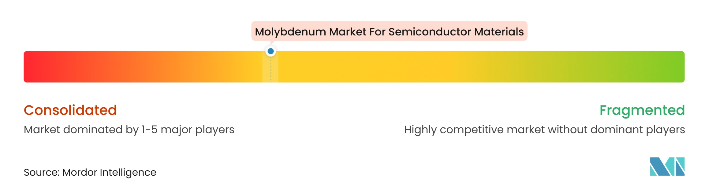
The molybdenum market for semiconductor materials is moderately concentrated, with the top five players including Plansee SE, JX Advanced Metals Corporation, Elmet Technologies, Materion Corporation, and Tosoh Corporation. Plansee SE, Elmet Technologies, and Konfoong Materials International Co., Ltd. also participate in the target supply chain. In high-purity products, material qualification, audit history, and process consistency limit the ability of new suppliers to gain customer approvals.
Leading suppliers are extending beyond physical vapor deposition targets into chemical vapor deposition and atomic layer deposition precursor chemistry. JX Advanced Metals Corporation completed its high-purity molybdenum dioxide dichloride production line in March 2026 and began shipments to advanced semiconductor customers. Materion Corporation reported commercial interest in its molybdenum atomic layer deposition portfolio during its 2025 memory ramp. Umicore identified molybdenum-based precursors as a next metal system in its Chemicals for Electronics development roadmap. Plansee SE also presented seed-layer stack and high-power impulse magnetron sputtering process improvements at TechCon 2024, showing that product differentiation depends on deposition knowledge as well as purity. The molybdenum market for semiconductor materials is therefore seeing competition extend across adjacent process steps for the same fab customers.
Opportunities are concentrated in 6N precursors for logic and dynamic random-access memory and in custom large-area molybdenum formats for advanced packaging. JX Advanced Metals Corporation and Materion Corporation have announced production-oriented capabilities in precursor chemistry. Konfoong Materials International Co., Ltd. is active in sputtering targets and competes in legacy-node applications. Elmet Technologies uses its integrated U.S. manufacturing position in procurement discussions related to domestic sourcing. Semiconductor Equipment and Materials International’s material expectations and fab quality systems continue to protect suppliers that have already completed qualification. The molybdenum market for semiconductor materials remains shaped by both technical specialization and customer approval barriers.
Leaders of Molybdenum Market For Semiconductor Materials
-
Plansee SE
-
JX Advanced Metals Corporation
-
Elmet Technologies
-
Materion Corporation
-
Tosoh Corporation
- *Disclaimer: Major Players sorted in no particular order
Molybdenum Market For Semiconductor Materials Companies Covered in this Report
- A.L.M.T. Corp.
- American Elements
- Edgetech Industries LLC
- Elmet Technologies
- H.C. Starck Solutions
- JX Advanced Metals Corporation
- Konfoong Materials International Co., Ltd.
- Kurt J. Lesker Company
- Materion Corporation
- Mitsui Kinzoku Co., Ltd.
- Plansee SE
- Plasmaterials, Inc.
- Stanford Advanced Materials
- Tosoh Corporation
- Umicore
Recent Industry Developments in Molybdenum Market For Semiconductor Materials
- October 2026: Merck KGaA inaugurated a new semiconductor materials manufacturing facility in Eumseong, South Korea, dedicated to producing molybdenum dioxide dichloride, a precursor used to deposit ultra-thin metal films during semiconductor manufacturing. The facility will supply advanced 3D NAND manufacturers across Asia, supporting the molybdenum market for semiconductor materials through increased regional production of high-purity molybdenum deposition materials.
- June 2025: JX Advanced Metals Corporation commenced full-scale production of chemical vapor deposition (CVD) and atomic layer deposition (ALD) materials at a new facility located at Toho Titanium's Chigasaki plant in Japan. The company's semiconductor materials portfolio includes molybdenum compounds, supporting the molybdenum market for semiconductor materials through expanded production capabilities for advanced thin-film deposition processes.
Scope of Report on Molybdenum Market For Semiconductor Materials
Molybdenum is a refractory metal characterized by its high melting point, thermal stability, and electrical conductivity. These properties make it suitable for semiconductor manufacturing, where high-purity molybdenum materials are used in thin-film deposition, interconnects, and specialized device components.
The Molybdenum Market for Semiconductor Materials is segmented by product type, application, semiconductor device type, and geography. By product type, the market is segmented into molybdenum sputtering targets, molybdenum powder, molybdenum foils and sheets, molybdenum compounds and precursors, and other product types. By application, the market is segmented into wafer fabrication, semiconductor packaging, and others. By semiconductor device type, the market is segmented into memory devices, logic devices and microprocessors, analog and power semiconductors, compound semiconductors, and other semiconductor devices. The report also covers the market size and forecasts for molybdenum for semiconductor materials across 16 countries. For each segment, the market sizing and forecasts have been done on the basis of value (USD).
Segmentation Overview
| Molybdenum Sputtering Targets |
| Molybdenum Powder |
| Molybdenum Foils and Sheets |
| Molybdenum Compounds and Precursors |
| Other Product Types |
| Wafer Fabrication |
| Semiconductor Packaging |
| Others |
| Memory Devices |
| Logic Devices and Microprocessors |
| Analog and Power Semiconductors |
| Compound Semiconductors |
| Other Semiconductor Devices |
| Asia-Pacific | China |
| India | |
| Japan | |
| South Korea | |
| ASEAN Countries | |
| Rest of Asia-Pacific | |
| North America | United States |
| Canada | |
| Mexico | |
| Europe | Germany |
| United Kingdom | |
| France | |
| Italy | |
| NORDIC Countries | |
| Russia | |
| Rest of Europe | |
| South America | Brazil |
| Argentina | |
| Rest of South America | |
| Middle East and Africa | Saudi Arabia |
| South Africa | |
| Rest of Middle East and Africa |
| By Product Type | Molybdenum Sputtering Targets | |
| Molybdenum Powder | ||
| Molybdenum Foils and Sheets | ||
| Molybdenum Compounds and Precursors | ||
| Other Product Types | ||
| By Application | Wafer Fabrication | |
| Semiconductor Packaging | ||
| Others | ||
| By Semiconductor Device Type | Memory Devices | |
| Logic Devices and Microprocessors | ||
| Analog and Power Semiconductors | ||
| Compound Semiconductors | ||
| Other Semiconductor Devices | ||
| By Geography | Asia-Pacific | China |
| India | ||
| Japan | ||
| South Korea | ||
| ASEAN Countries | ||
| Rest of Asia-Pacific | ||
| North America | United States | |
| Canada | ||
| Mexico | ||
| Europe | Germany | |
| United Kingdom | ||
| France | ||
| Italy | ||
| NORDIC Countries | ||
| Russia | ||
| Rest of Europe | ||
| South America | Brazil | |
| Argentina | ||
| Rest of South America | ||
| Middle East and Africa | Saudi Arabia | |
| South Africa | ||
| Rest of Middle East and Africa | ||
Key Questions Answered in the Report
What is the size of the molybdenum market for semiconductor materials?
The molybdenum market for semiconductor materials industry size was valued at USD 413.72 million in 2026 and is estimated to grow from USD 443.88 million in 2027 to reach USD 638.14 million by 2032, at a CAGR of 7.53% during the forecast period (2027-2032).
What is driving demand for molybdenum in semiconductor manufacturing?
Leading-edge fab expansion, higher purity requirements, and the use of molybdenum in scaled contacts and word lines support demand.
Which product type held the largest share in 2026?
Molybdenum sputtering targets held a 52.11% share in 2026 because physical vapor deposition remains widely used in front-end wafer processing.
Which application is expected to grow fastest through 2032?
Semiconductor packaging is projected to advance at an 8.34% CAGR through 2032 as chiplets, fan-out packaging, and 3D integration expand.