
Size and Share of Japan Solder Materials Market In Semiconductor Industry
Market Overview
| Study Period | 2021 - 2032 |
|---|---|
| Forecast Data Period | 2027 - 2032 |
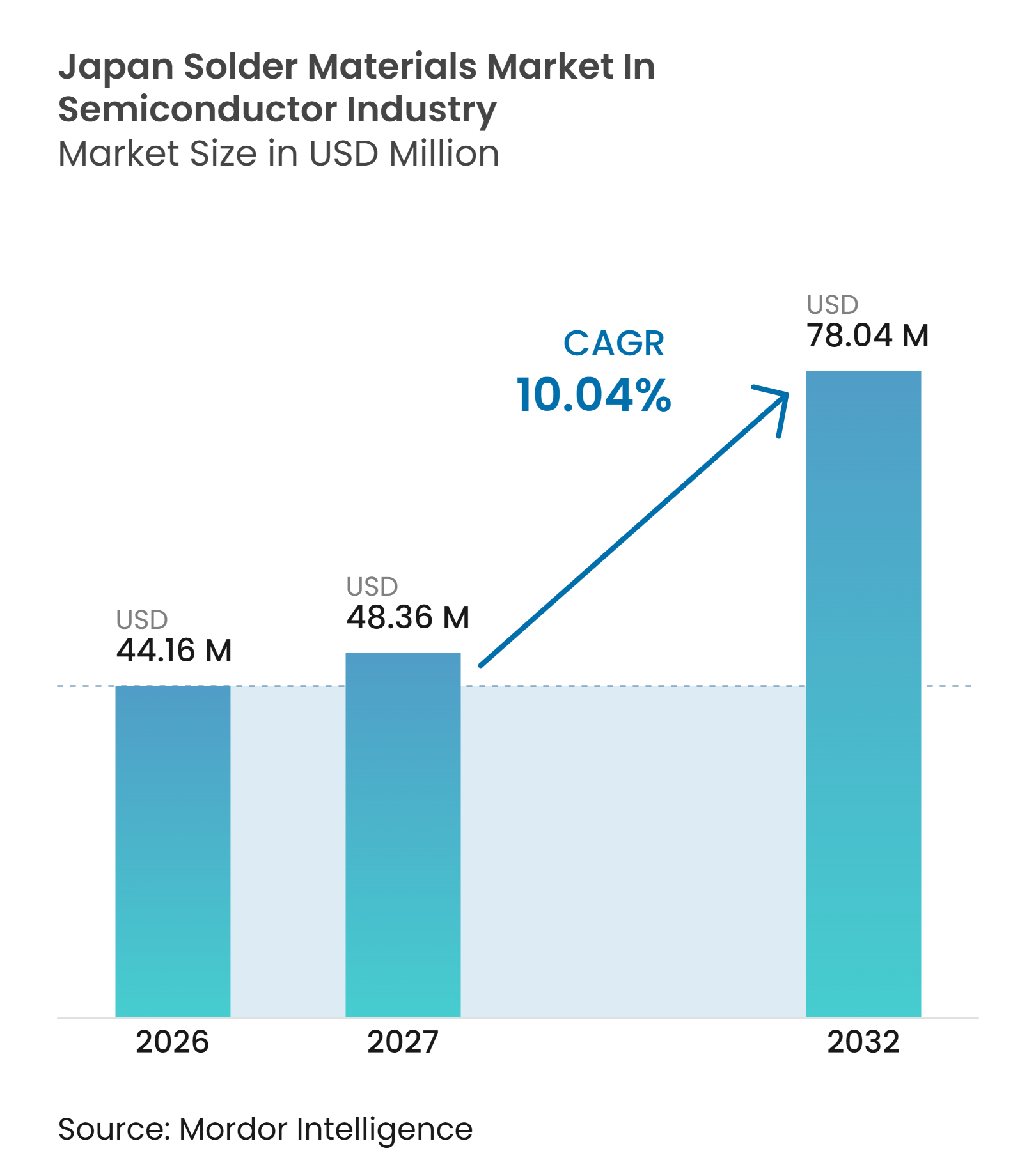
| Base Year Market Size (2026) | USD 44.16 Million |
| Market Size (2027) | USD 48.36 Million |
| Market Size (2032) | USD 78.04 Million |
| Growth Rate (2027 - 2032) | 10.04 % |
| Market Concentration | Medium |
Major Players *Disclaimer: Major Players sorted in no particular order Image © Mordor Intelligence. Reuse requires attribution under CC BY 4.0. | |
Analysis of Japan Solder Materials Market In Semiconductor Industry by Mordor Intelligence
The Japan solder materials market in semiconductor industry size is projected to expand from USD 44.16 million in 2026 and USD 48.36 million in 2027 to USD 78.04 million by 2032, registering a CAGR of 10.04% between 2027 to 2032. Advanced packaging is directing more material value toward wafer-level bumping, flip-chip assembly, and BGA processes than conventional board-level soldering. Domestic semiconductor investment is widening the addressable base for qualified formulations, especially in Kyushu and Hokkaido. AI accelerators, chiplets, and high-bandwidth memory packages need tighter interconnect control, which raises demand for fine powders, microballs, and process-specific flux systems. Suppliers are competing through alloy design, application engineering, local technical support, and qualification history. The Japan solder materials market in semiconductor industry also faces material-cost exposure and increasing competition from copper pillar, hybrid bonding, and sintered joining approaches at the finest pitches.
Key Report Takeaways
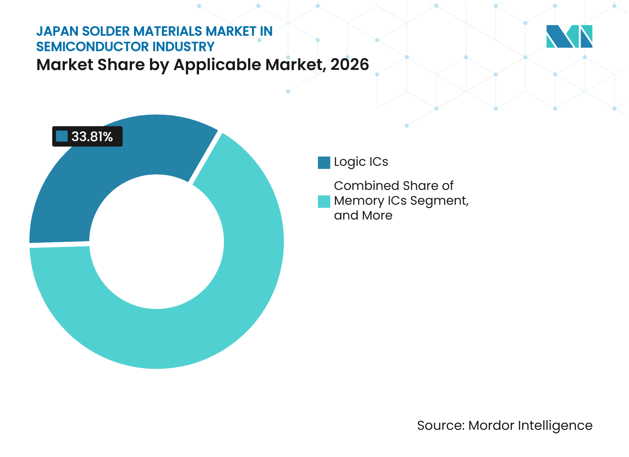
- By applicable market, Logic ICs held 33.81% of revenue of the Japan solder materials market in semiconductor industry in 2026, while Memory ICs are projected to expand at a CAGR of 10.44% through 2032.
- By product form, solder paste held 40.26% of revenue of the Japan solder materials market in semiconductor industry in 2026, while solder balls and spheres are projected to expand at a CAGR of 10.57% through 2032.
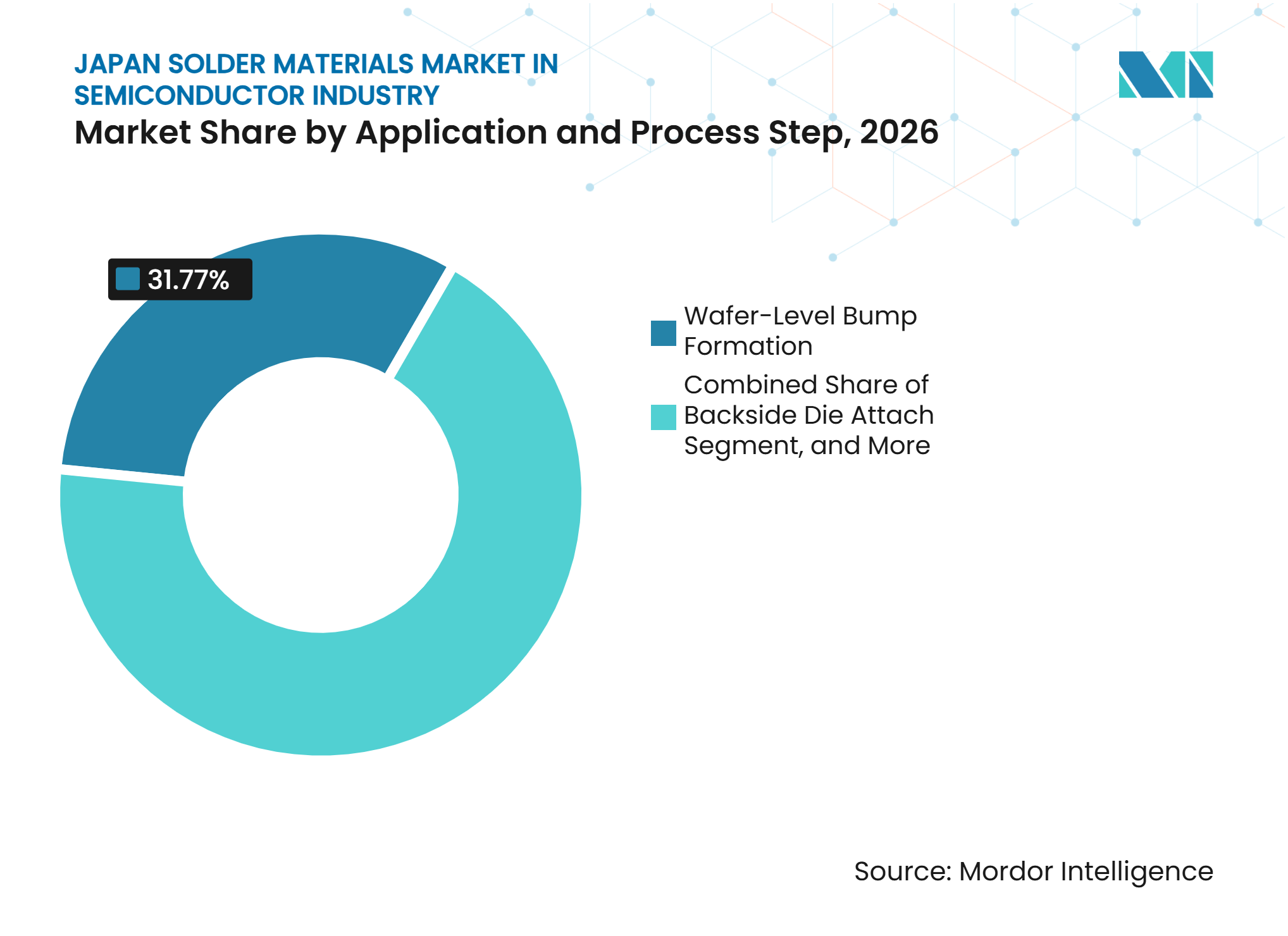
- By application and process step, wafer-level bump formation accounted for 31.77% of the Japan solder materials market in semiconductor industry size in 2026 and is projected to expand at a CAGR of 10.82% through 2032.
- By geography, Kanto held 38.48% of revenue in 2026, while Kyushu is projected to expand at a CAGR of 10.74% through 2032.
Note: Market numbers in this report are based on Mordor Intelligence's proprietary estimation framework, which combines nine months of actuals with Q4 projections for base year 2026.
Market Trends and Insights
Drivers Impact Analysis of Japan Solder Materials Market in Semiconductor Industry*
| Driver | (~) % Impact on CAGR Forecast | Geographic Relevance | Impact Timeline |
|---|---|---|---|
| AI, HPC, and HBM Package Complexity | +2.5% | Global, with core demand in Kanto and Kyushu | Short term (≤ 2 years) |
| Japan-Led Expansion of Precision Semiconductor Packaging | +2.0% | Kyushu, Hokkaido, National | Medium term (2-4 years) |
| Lead-Free and Low-Temperature Alloy Conversion | +1.5% | Global, with early gains in Kanto and Chubu | Medium term (2-4 years) |
| Fine-Pitch Miniaturization and Ultra-Fine Powder Demand | +1.2% | Kanto, Kyushu | Long term (≥ 4 years) |
| Automotive Power Semiconductor Reliability Requirements | +0.9% | Chubu, Kansai | Medium term (2-4 years) |
| Domestic Supply-Chain Resilience and Local Qualification | +0.6% | National, with early gains in Kanto, Kyushu, and Hokkaido | Long term (≥ 4 years) |
| Source: Mordor Intelligence | |||
AI, HPC, and HBM Package Complexity
Advanced packages used in AI accelerators need solder materials that perform beyond conventional assembly grades. CoWoS, 2.5D interposers, and HBM stacks require controlled oxidation, stable flux behavior, and precise particle distributions at sub-100-μm bump pitches. Demand is concentrated in high-volume programs that require complex package designs and repeatable material performance. That concentration gives qualified suppliers recurring sales during the life of a customer program, but it also raises the importance of securing qualification early. JASM’s first Kumamoto fab reached full capacity from late 2024, while the planned 3nm process at Plant 2 reinforces Japan’s role in advanced-node manufacturing. This production base makes the Japan solder materials market in semiconductor industry more closely connected to AI packaging demand than general electronics assembly demand.
Japan-Led Expansion of Precision Semiconductor Packaging
Japan’s semiconductor policy and investment cycle are expanding demand for semiconductor-grade joining materials. METI approved a revised production plan for JASM’s second Kumamoto facility, which targets 6,000 300-mm wafers per month in the fourth quarter of 2028 and investment of at least USD 15.7 billion.[1] Rapidus demonstrated 2nm gate-all-around transistor wafers in Hokkaido during July 2025 after beginning pilot-line operations in April 2025.[2] These projects create qualification windows for suppliers of solder, bonding, and related process materials. JASM’s local procurement goals of 50% domestic indirect-materials content by 2026 and 60% by 2030 add an incentive for suppliers with local production or technical service capability. The Japan solder materials market in semiconductor industry benefits when local suppliers can meet the same reliability and traceability requirements as established global suppliers.
Lead-Free and Low-Temperature Alloy Conversion
Lead-free solder conversion is moving beyond basic regulatory compliance toward thermal management in advanced packages. J-MOSS and the EU RoHS framework supported the broad use of SAC305, which has a liquidus temperature of 217°C. Large BGA packages for AI and HPC systems are increasing interest in bismuth-free and indium-containing low-temperature options because warpage and electromigration performance are material-selection concerns. The Japan Welding Engineering Society is working on ISO 9453 lead-free solder alloy standards and IEC/TC 91 test methods for sintered joining materials.[3] KOKI’s Sn-Bi product line has a melting point of 138°C, while Indium Corporation’s DFLT paste uses a 210°C peak reflow profile and targets large-format HPC BGA requirements. These developments widen the role of formulation expertise in the Japan solder materials industry.
Fine-Pitch Miniaturization and Ultra-Fine Powder Demand
Bump pitches below 50 μm are moving demand from Type 4 and Type 5 powders toward Type 6 and Type 7 grades. This shift requires tighter control in atomization, particle classification, and low-alpha processing. Ultrafine powders and sub-50-μm solder balls carry higher value than standard grades because their manufacturing and quality requirements are more demanding. Research presented at IEEE ECTC in 2025 found that reliable copper pillar bumps on ENEPIG substrates for automotive FCBGA applications depend on careful tin-silver solder-cap composition control. Wafer bumping for silicon interposers and RDL fan-out packages is therefore becoming an important route for advanced materials demand. Established suppliers in the Japan solder materials market in semiconductor industry are better placed where they can combine powder-metallurgy capability with long-standing customer co-development.
Restraints Impact Analysis of Japan Solder Materials Market in Semiconductor Industry*
| Restraint | (~) % Impact on CAGR Forecast | Geographic Relevance | Impact Timeline |
|---|---|---|---|
| High Qualification Cost and Long Customer Approval Cycles | -1.8% | Global, most acute in Kanto and Kyushu | Short term (≤ 2 years) |
| Raw-Material Price Volatility | -1.5% | Global | Short term (≤ 2 years) |
| Thermal-Fatigue and Void-Control Risk at Fine Pitches | -0.9% | Kanto, Kyushu | Medium term (2-4 years) |
| Substitution by Copper Pillars, Hybrid Bonding, and Sintered Materials | -0.7% | Kanto, Kyushu | Long term (≥ 4 years) |
| Source: Mordor Intelligence | |||
High Qualification Cost and Long Customer Approval Cycles
Semiconductor-grade solder and sinter materials undergo extensive qualification before production use. Testing covers oxidation, sphere-size distribution, flux rheology, void rates, intermetallic growth, thermal fatigue, and electromigration. A qualification program with an OSAT or IDM may take 12 to 18 months and requires engineering work from both the supplier and the customer. Domestic procurement requirements do not remove the need to match the performance of globally qualified materials. A defect involving bridging, non-wet opens, or inconsistent bump height can restart the approval process. This favors incumbents in the Japan solder materials market in semiconductor industry that can support the cost, documentation, and technical service required for repeated qualification work.
Raw-Material Price Volatility
Tin and silver are the main metal inputs in lead-free solder alloys, leaving suppliers exposed to changes in raw-material costs. Supply disruption, export-policy uncertainty, and changes in metal demand can affect the cost of these inputs. Silver price movements also affect alloy economics because SAC305 contains 3% silver. The silver content can represent a substantial share of total metal cost within the alloy. Advance-purchase contracts and strict lot traceability limit a supplier’s ability to reformulate quickly in response to price changes. These conditions can compress margins or lead to customer price discussions within the Japan solder materials market in semiconductor industry.
*Our forecasts treat driver/restraint impacts as directional, not additive. The impact forecasts reflect baseline growth, mix effects, and variable interactions.
Japan Solder Materials Market In Semiconductor Industry Segment Analysis
By Applicable Market:
Logic IC Demand Supports Revenue While Memory ICs Lead ExpansionLogic ICs held 33.81% of the Japan solder materials market share in 2026. Wafer-level and flip-chip packaging for logic devices create demand in technically demanding process steps. AI accelerators may require several thousand solder bumps at pitches below 100 μm, raising both the specification level and value of materials used. ADEKA noted the transition in back-end processes from 2D solder-based microbumps to 3D hybrid bonding for next-generation logic stacking. Solder and direct copper bonding are expected to coexist across different process layers for much of the forecast period. The Japan solder materials market in semiconductor industry remains exposed to this changing mix of joining methods rather than a single technology path.
Memory ICs are projected to expand at a CAGR of 10.44% from 2027 to 2032. HBM packages use 4 to 12 DRAM dies, increasing the number and difficulty of interconnects needed per chipset. Compound semiconductors and power devices require high-temperature die-attach materials that withstand repeated thermal cycling from -40°C to 150°C or higher. Analog ICs, sensors, MEMS, RF devices, and optical packages also draw on distinct alloy and flux requirements. Gold-tin eutectic solder remains relevant for reliable laser and photonic-chip attachment. A broad formulation portfolio helps suppliers serve these different device classes without relying on a single end-use market.


By Product Form:
Solder Paste Retains Leadership While Solder Balls and Spheres AccelerateSolder paste held 40.26% of Japan solder materials market size by product form in 2026. It remains important for screen-printing and stencil-jetting used in wafer-level bumping and package-on-board processes. The product mix is shifting from Type 4 and Type 5 grades toward Type 6 and Type 7 fine-powder pastes and jettable products for features below 50 μm. Indium Corporation presented no-clean solder pastes for miniaturized assemblies at APEX 2026, identifying cleaning compatibility and flux selection as relevant considerations for smaller features. These requirements support demand for application-specific paste development. The Japan solder materials market in the semiconductor industry depends on paste suppliers maintaining lot consistency while adapting to finer pitches.
Solder balls and spheres are projected to expand at a CAGR of 10.57% from 2027 to 2032. BGA ball attachment and micro-solder ball use in flip-chip and wafer-level processes are central sources of demand. Sub-50-μm microballs used in flip-chip and silicon-interposer packaging have higher value than standard BGA balls. Their adoption is tied to qualification cycles at JASM and Rapidus. Preforms support specialized die attachment, package sealing, and high-reliability applications where contamination must be controlled. Wires, fluxes, and externally supplied powder serve rework, selective soldering, and custom alloy formulation needs, creating a split between commodity volumes and high-specification products.
By Application and Process Step:
Wafer-Level Bumping Leads Both Scale and ExpansionWafer-level bump formation accounted for 31.77% of the Japan solder materials market size in 2026. It is also projected to expand at a CAGR of 10.82% through 2032. Chiplet architectures used in AI and HPC packages concentrate interconnect complexity at the wafer level before final assembly. This raises demand for ultrafine powders and microballs that were less important in earlier device generations. Applied Materials stated that commercial Cu-Cu hybrid bonding is used at pitches below 9 μm, leaving solder bumping relevant across a broader 10-100-μm range. This range sustains wafer-level solder demand even as hybrid bonding progresses at the finest pitches.
Flip-chip die-to-substrate interconnection is the second-largest process step by revenue. Copper pillar solder-capped bumps are widely used in FCBGA and FC-CSP packages for logic and memory devices. Package-to-board BGA and CSP attachment generates large ball volumes, though the value per connection is lower than for wafer-level applications. Backside die attachment and package sealing serve power devices and hermetic applications, where high-antimony solder and sintered silver compete. JSAE technical work in 2026 highlighted the importance of nondestructive and destructive characterization for BGA joint reliability as board density increases. Process guidance and material selection are therefore integral to supplier positioning.
Geography Analysis
Kanto
Kanto remains a major regional hub for Japan's solder materials market, supported by the concentration of semiconductor packaging facilities, materials research and development centres, equipment manufacturers, and supplier headquarters across Tokyo, Kanagawa, and neighbouring prefectures. Senju Metal Industry, Tamura Corporation, Nippon Micrometal, and NIHON SUPERIOR have significant operations in the region. International materials companies also maintain Japan-focused engineering and application support teams in the area. NEDO's initiatives to strengthen semiconductor supply-chain resilience in Kanto cover silicon wafers, packaging materials, and process consumables. The region's participation in international standards and research activities, including ISO 9453 and IEC/TC 91, further reinforces its technical capabilities. This established ecosystem supports demand for solder materials suppliers offering specialised formulations, application engineering, and close customer collaboration.
Kyushu
Kyushu is emerging as an important growth centre for Japan's solder materials market, primarily due to the expansion of advanced semiconductor manufacturing around Kumamoto. JASM's first fabrication facility commenced mass production and achieved full production capacity ahead of schedule. The company is also advancing plans for a second facility focused on advanced process technologies, with production targeted to begin in the coming years. These investments are strengthening the regional semiconductor supply chain and creating opportunities for domestic and international solder materials suppliers. Local procurement initiatives provide an advantage to suppliers capable of establishing technical service capabilities, securing customer qualifications, and supporting multiple sourcing requirements. Demand opportunities extend across bump formation, solder ball attachment, and package-sealing applications, particularly as advanced logic manufacturing and associated packaging activities expand in the region.
Kansai, Chubu, Hokkaido, and Other Regions
Kansai supports power-semiconductor packaging, analog IC assembly, and R&D activity across Osaka, Kyoto, and Hyogo. Its industrial base links solder demand to automotive power modules and compound semiconductor operations. Chubu is closely tied to automotive electronics supply chains around Nagoya, including Toyota and Denso. JSAE technical sessions have highlighted tighter reliability requirements for solder joints in next-generation automotive control units. Hokkaido is an emerging location, as Rapidus demonstrated a 2nm gate-all-around transistor wafer in July 2025 and plans to begin mass production with back-end capability in the second half of fiscal 2027. Tohoku and adjacent Chugoku maintain demand connected to memory packaging and test operations. Chugoku, Shikoku, and Okinawa support smaller localized assembly and niche packaging activities. Across these locations, the Japan solder materials market in semiconductor industry gains incremental demand while Kyushu and Kanto remain the principal locations for advanced-package material qualification.
Competitive Landscape
Market Concentration
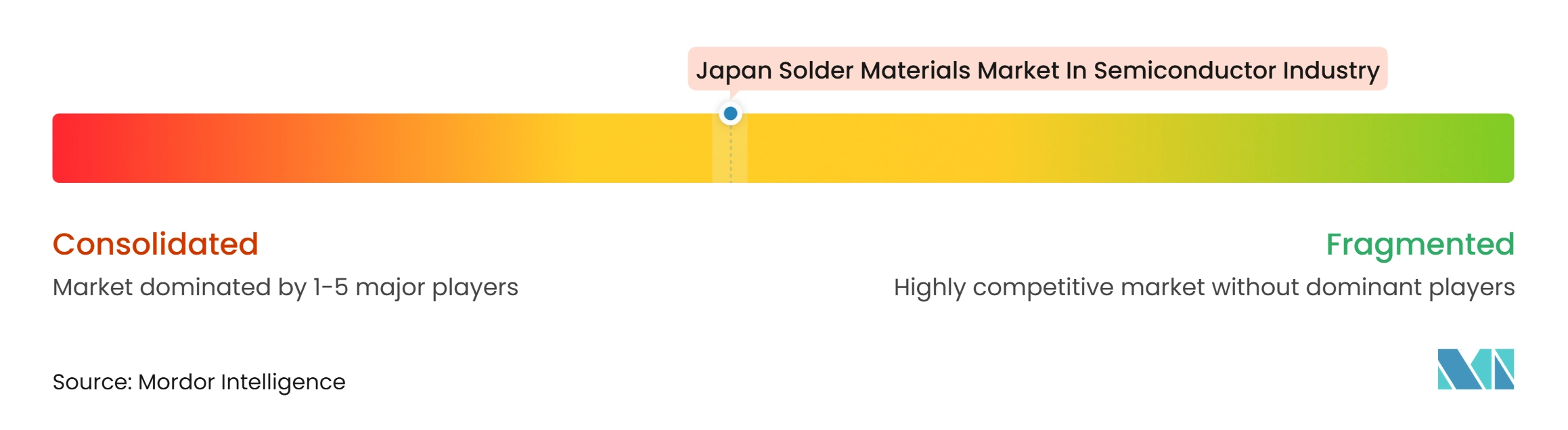
The Japan solder materials market in semiconductor industry is moderately concentrated among domestic incumbents and global material suppliers. Senju Metal Industry, Tamura Corporation, KOKI, and Nippon Micrometal benefit from established customer relationships and local technical service. Their positions are also supported by experience in customer co-development and participation in standards activities. MacDermid Alpha Electronics Solutions, Heraeus Electronics, and Indium Corporation compete across solder paste, sintered silver, low-temperature formulations, and thermal-interface materials. The competitive basis is increasingly tied to alloy intellectual property, reliability results, and process support. Suppliers must prove performance across advanced packaging, automotive, and power-device requirements.
Heraeus Electronics, MacDermid Alpha, and Henkel prevailed in patent infringement and patent nullity proceedings against Senju Group in Germany during February 2025 over the Innolot high-reliability lead-free solder alloy formulation. The outcome underlines the importance of protected alloy chemistry in high-reliability solder applications. Indium Corporation has promoted its DFLT bismuth-free, indium-containing low-temperature solder paste for large-format AI package BGA assemblies. KOKI provides low-temperature soldering products that address reflow temperature needs. These moves show that suppliers are seeking differentiation through specific performance limits rather than through production scale alone. Local technical response and documentation support remain important when customers qualify new materials.
The strongest openings are in ultrafine powders, sub-50-μm solder balls, and low-temperature formulations for 3nm packaging programs. Sintered copper also represents an emerging alternative for large-area power die attachment. MacDermid Alpha presented BondPad, a sintered-film copper-foil solution for silicon carbide power packages, during 2026. The company reported more than 75,000 power cycles in its stated test conditions, compared with 2,500 cycles for aluminum wirebond references. Hybrid bonding is expected to replace some microbump solder use at the smallest pitches, but solder retains a role across the wider 10-100-μm range. Suppliers in the Japan solder materials market in semiconductor industry can protect their position by pairing qualified local supply with application-matched engineering. In the Japan solder materials market in semiconductor industry, this places technical support and local qualification alongside formulation design as practical competitive requirements. The competitive outlook therefore combines incumbent advantage with targeted opportunity in new joining formats.
Leaders of Japan Solder Materials Market In Semiconductor Industry
-
Senju Metal Industry Co., Ltd.
-
TAMURA CORPORATION
-
KOKI COMPANY LIMITED
-
Indium Corporation
-
Heraeus Electronics
- *Disclaimer: Major Players sorted in no particular order
Japan Solder Materials Market In Semiconductor Industry Companies Covered in this Report
- Senju Metal Industry Co., Ltd.
- TAMURA CORPORATION
- KOKI COMPANY LIMITED
- Indium Corporation
- Heraeus Electronics
- MacDermid Alpha Electronics Solutions
- SHENMAO Technology Inc.
- DUKSAN Hi-Metal Co., Ltd.
- Nippon Micrometal Corporation
- NIHON SUPERIOR CO., LTD.
- AIM Solder
- Harima Chemicals Group, Inc.
- Mitsui Kinzoku Company, Limited
- Henkel AG & Co. KGaA
- Element Solutions Inc.
- Kester
- Qualitek International, Inc.
- Materion Corporation
- PFARR Stanztechnik GmbH
- Mitsui Mining and Smelting Co., Ltd.
Recent Industry Developments in Japan Solder Materials Market In Semiconductor Industry
- November 2026: TSMC Senior Vice President Kevin Zhang confirmed at the World Management Meeting, Nikkei-IMD, Tokyo, that the second Kumamoto fab, Phase 2, will deploy the 3nm process, and that TSMC plans to establish a joint venture with Sony for physical AI image sensor production. This announcement reinforces Kyushu's role as a primary advanced logic packaging hub and extends the domestic solder-materials demand runway well beyond the initial JASM Phase 1 program.
- November 2026: MacDermid Alpha Electronics Solutions presented BondPad, an Argomax sintered-film copper-foil solution for die topside attach in silicon carbide power packages, at electronica 2026 in Munich. Under power-cycling test conditions, 180A, ΔT = 110°C, Tj,max = 175°C, BondPad achieved over 75,000 cycles against 2,500 cycles for conventional aluminum wirebond references, signaling that sintered copper interconnects are approaching commercial readiness and intensifying displacement pressure on high-temperature solder in power device applications.
- October 2026: Japan's Ministry of Economy, Trade and Industry formally approved TSMC/JASM's revised plan to manufacture 3nm logic semiconductors at Kumamoto Plant 2, with investment of at least USD 15.7 billion and an initial monthly capacity target of 6,000 300-mm wafers planned for the fourth quarter of 2028. The approval requires JASM to source a specified share of indirect packaging materials, including solder consumables, from domestic Japanese suppliers, creating a direct and time-bounded market opportunity.
- September 2026: Indium Corporation presented its DFLT bismuth-free, indium-containing low-temperature solder paste at the IMAPS Symposium 2026. DFLT achieves a 210°C peak reflow temperature, electromigration performance exceeding BiSnAg alloys by 2 orders of magnitude in drop-shock testing, and overall reliability comparable to or above SAC305, targeting warpage-driven challenges in large-format AI package BGA assemblies.
Scope of Report on Japan Solder Materials Market In Semiconductor Industry
The Japan Solder Materials Market in the Semiconductor Industry refers to the national market for solder-based interconnect materials used in semiconductor packaging, wafer-level assembly, flip-chip bonding, and advanced IC packaging, including solder balls, solder paste, solder wire, solder preforms, fluxes, and specialized alloys serving Japan’s semiconductor packaging, automotive electronics, precision machinery, and high-reliability industrial electronics sectors.
Japan Solder Materials Market in Semiconductor Industry Report is Segmented by Applicable Market (Logic ICs, Memory ICs, Compound Semiconductors and Power Devices, Analog ICs, Sensors, MEMS and RF Devices, and Optical and Photonic Devices), Product Form (Solder Paste, Solder Balls and Spheres, Solder Preforms, Solder Wire, Solder Fluxes, Standalone, and Solder Powder, Externally Sold), and Application and Process Step (Wafer-Level Bump Formation, Die-to-Substrate Interconnection, Conventional Flip-Chip, Package-to-Board Interconnection, BGA and CSP Ball Attach, Backside Die Attach, and Package Sealing and Component Attachment). The Market Forecasts Are Provided in Terms of Value (USD).
Segmentation Overview
| Logic ICs |
| Memory ICs |
| Compound Semiconductors and Power Devices |
| Analog ICs |
| Sensors, MEMS and RF Devices |
| Optical and Photonic Devices |
| Solder Paste |
| Solder Balls and Spheres |
| Solder Preforms |
| Solder Wire |
| Solder Fluxes, Standalone |
| Solder Powder, Externally Sold |
| Wafer-Level Bump Formation |
| Die-to-Substrate Interconnection, Conventional Flip-Chip |
| Package-to-Board Interconnection, BGA and CSP Ball Attach |
| Backside Die Attach |
| Package Sealing and Component Attachment |
| By Applicable Market | Logic ICs |
| Memory ICs | |
| Compound Semiconductors and Power Devices | |
| Analog ICs | |
| Sensors, MEMS and RF Devices | |
| Optical and Photonic Devices | |
| By Product Form | Solder Paste |
| Solder Balls and Spheres | |
| Solder Preforms | |
| Solder Wire | |
| Solder Fluxes, Standalone | |
| Solder Powder, Externally Sold | |
| By Application and Process Step | Wafer-Level Bump Formation |
| Die-to-Substrate Interconnection, Conventional Flip-Chip | |
| Package-to-Board Interconnection, BGA and CSP Ball Attach | |
| Backside Die Attach | |
| Package Sealing and Component Attachment |
Key Questions Answered in the Report
What is the Japan solder materials market in semiconductor industry size?
The Japan solder materials market in semiconductor industry is projected to expand from USD 44.16 million in 2026 and USD 48.6 million in 2027 to USD 78.05 million by 2032, at a CAGR of 10.06%.
What is driving demand for semiconductor solder materials in Japan?
AI, HPC, and HBM package complexity, domestic fab investment, lead-free alloy conversion, and fine-pitch interconnect requirements are supporting demand.
Which product form leads semiconductor solder demand in Japan?
Solder paste held 40.26% of product-form revenue in 2026 because it is used in wafer-level bumping and package-on-board processes.
Which application is expanding fastest for solder materials used in Japanese semiconductor packaging?
Wafer-level bump formation led application revenue with 31.77% in 2026 and is projected to expand at a CAGR of 10.82% through 2032.
Which Japanese region offers the strongest expansion potential for semiconductor solder suppliers?
Kyushu is projected to expand at a CAGR of 10.74% through 2032, supported by JASM activity in Kumamoto and associated supplier qualification opportunities.
How are hybrid bonding and sintered materials changing the outlook for solder suppliers?
These alternatives can replace solder at the smallest pitches and in some power-device applications, while solder remains relevant across the broader 10-100-?m interconnect range.