Graphene Infrared Imaging Sensors Market Size and Share
Market Overview
| Study Period | 2020 - 2031 |
|---|---|
| Market Size (2026) | USD 54.91 Million |
| Market Size (2031) | USD 276.59 Million |
| Growth Rate (2026 - 2031) | 38.18 % |
| Fastest Growing Market | Asia-Pacific |
| Largest Market | Asia-Pacific |
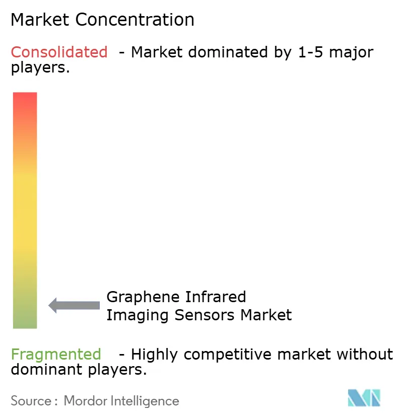
| Market Concentration | Low |
Major Players *Disclaimer: Major Players sorted in no particular order Image © Mordor Intelligence. Reuse requires attribution under CC BY 4.0. | |
Graphene Infrared Imaging Sensors Market Analysis by Mordor Intelligence
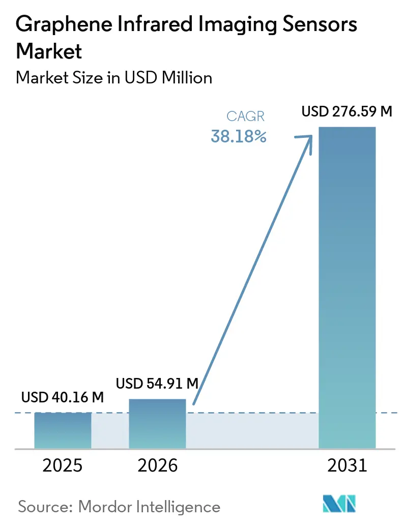
The Graphene infrared imaging sensors market size was valued at USD 40.16 million in 2025 and estimated to grow from USD 54.91 million in 2026 to reach USD 276.59 million by 2031, at a CAGR of 38.18% during the forecast period (2026-2031). The graphene infrared imaging sensors market is entering a volume-scaling phase as wafer processing becomes more repeatable. A 200 mm CMOS-compatible GFET-quantum dot detector platform demonstrated yields that support commercial manufacturing rather than laboratory-only production. This development improves the case for graphene devices where buyers need lower cost and room-temperature operation. Procurement activity in defense, security, and industrial imaging is also favoring compact sensors that reduce cooling, power, and system integration needs. Supply chain concerns regarding established compound semiconductors are prompting government buyers to consider graphene-on-CMOS platforms as an additional sourcing option.
Key Report Takeaways
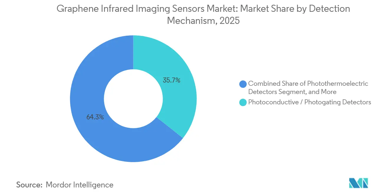
- By detection mechanism, photoconductive and photogating detectors held 35.67% of the graphene infrared imaging sensors market share in 2025, while photothermoelectric detectors are projected to expand at a 40.74% CAGR through 2031.
- By spectral range, short-wave infrared held 32.34% share in 2025, while mid-wave infrared is projected to expand at a 41.89% CAGR through 2031.
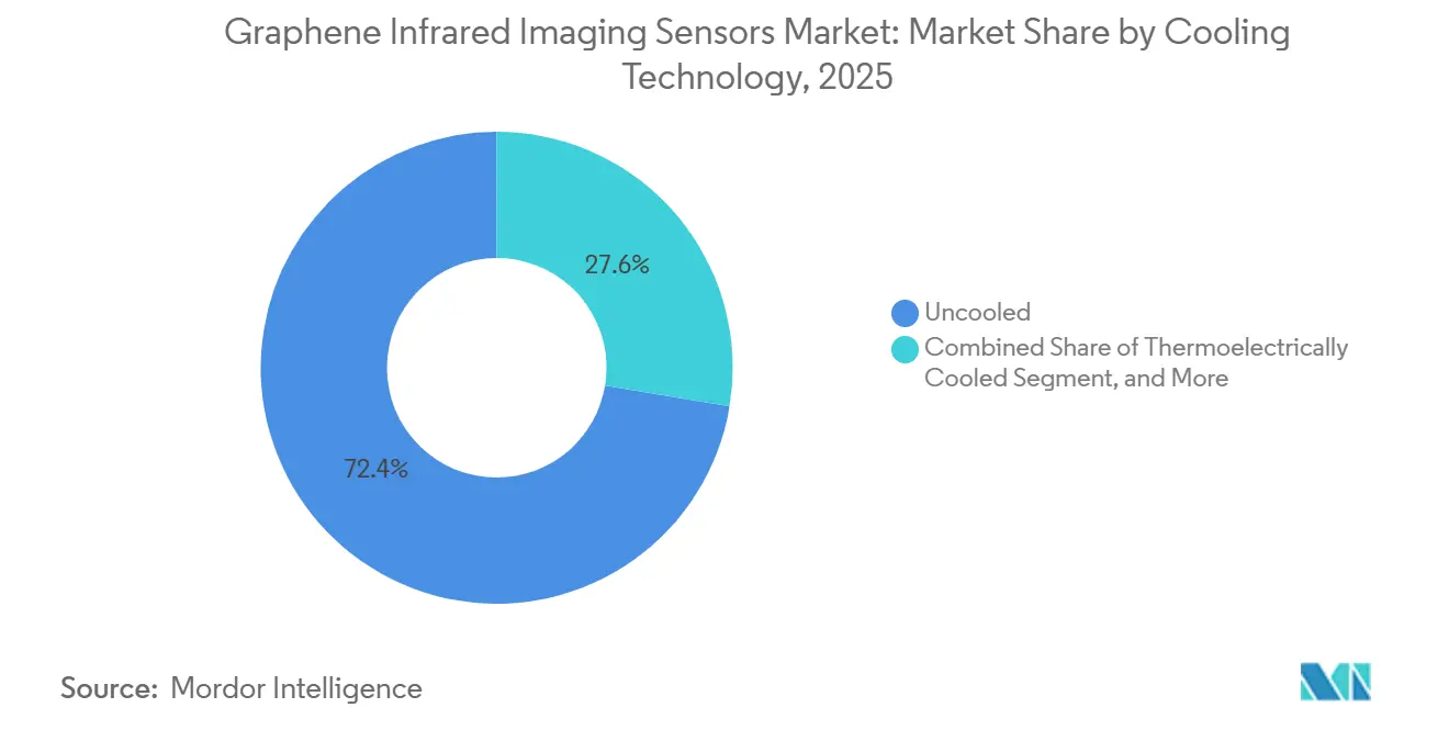
- By cooling technology, uncooled sensors held 72.39% share in 2025, while thermoelectrically cooled sensors are projected to expand at a 41.53% CAGR through 2031.
- By application, defense, security, and surveillance accounted for 38.92% in 2025 and are projected to expand at a 40.67% CAGR through 2031.
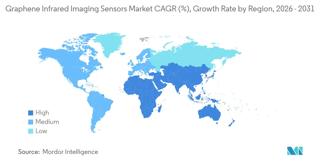
- By geography, Asia-Pacific held 34.65% share in 2025 and is projected to expand at a 41.12% CAGR through 2031.
Note: Market size and forecast figures in this report are generated using Mordor Intelligence’s proprietary estimation framework, updated with the latest available data and insights as of January 2026.
Global Graphene Infrared Imaging Sensors Market Trends and Insights
Drivers Impact Analysis*
| Driver | (~) % Impact on CAGR Forecast | Geographic Relevance | Impact Timeline |
|---|---|---|---|
| Falling Graphene-On-Wafer Integration Costs | +7.5% | Global, with concentrated gains in the EU foundry ecosystem and East Asian manufacturing centers | Medium term (2-4 years) |
| Demand for Low-Cost Uncooled SWIR Imaging | +6.5% | Global, with early deployment in North American and EU industrial machine vision and Asia-Pacific automotive applications | Short term (≤ 2 years) |
| Expansion of AI-Enabled Machine Vision | +5.5% | Global, especially Asia-Pacific manufacturing hubs and North American robotics and logistics sectors | Short term (≤ 2 years) |
| Growth in Defense and Automotive Night Vision | +4.8% | North America, Europe, and Asia-Pacific defense procurement markets | Medium term (2-4 years) |
| Wafer-Scale GFET-Quantum Dot Manufacturing | +4.1% | EU 2D Pilot Line initiative, East Asian semiconductor hubs, and nascent North American capacity | Medium term (2-4 years) |
| Edge Spectral Intelligence in Compact Devices | +3.2% | Global, with consumer electronics demand in East Asia and North America | Long term (≥ 4 years) |
| Source: Mordor Intelligence | |||
Falling Graphene-On-Wafer Integration Costs
Graphene integration costs have been a central barrier to broader sensor adoption. AMO GmbH opened its fourth multi-project wafer run under the EU 2D Pilot Line in 2026. The program shares device costs among several design customers and reduces the cost of foundry-grade prototyping. A 2025 study reported a 96-98% device yield across 3,200 mm production runs, demonstrating reproducible batch processing. AMO also reported a scalable aluminum oxide dielectric route that remained compatible with CMOS back-end thermal limits.[1]AMO GmbH, “Scalable Dielectric Integration on Graphene for Next-Generation Electronic Devices,” AMO GmbH, amo.de. The graphene infrared imaging sensors market can therefore use existing silicon manufacturing flows without requiring entirely separate fabrication infrastructure. This improves the production case for the graphene infrared imaging sensors market.
Demand for Low-Cost Uncooled SWIR Imaging
Conventional indium gallium arsenide SWIR sensors have remained expensive for many volume-sensitive uses. Emberion introduced an ultra-low-cost SWIR sensor in 2024 with a production target of EUR 50 per unit (USD 54 per unit) at large volumes. Its wafer-level packaging process supports up to 100 sensors per 8-inch wafer. Emberion completed an initial packaging development and testing round with a 100% bond yield across a full wafer in 2025. Lower device costs could extend SWIR deployment into automotive systems and consumer devices. The graphene infrared imaging sensors market would also gain from the manufacturing learning effects associated with these higher unit volumes. This gives the graphene infrared imaging sensors market an additional route to lower unit costs.
Expansion of AI-Enabled Machine Vision
Machine vision systems increasingly need information that visible-band cameras cannot capture. Graphene infrared detectors can be integrated with CMOS imagers without additional epitaxial growth steps. A 2025 study demonstrated a graphene- and chromium oxychloride-based optical synapse that detected wavelengths from 520 to 2,000 nm. PMC The device achieved more than 98% accuracy in infrared signal orientation detection using in situ reservoir computing. PMC Processing at the sensor can reduce data transfers for robotic and surveillance equipment. This capability supports the graphene infrared imaging sensors market, where compact systems must operate with constrained bandwidth and power. It also broadens the graphene infrared imaging sensors market for sensor-level computing.
Growth in Defense and Automotive Night Vision
Defense buyers are prioritizing compact uncooled infrared sensors for unmanned platforms. The US Army's DUTCH program focuses on improved uncooled thermal sensing and smaller size, weight, power, and cost requirements. The European Defense Fund-backed SPIRIT program was announced in 2026 to develop an EU supply chain for next-generation infrared detectors. The project has a EUR 39.16 million (USD 43.1 million) budget and involves 15 partners from 9 European countries. Automotive testing can also generate vibration, thermal-cycle, and humidity data relevant to defense qualification. The graphene infrared imaging sensors market benefits when these programs reduce the financial risk of early product validation.
Restraints Impact Analysis*
| Restraint | (~) % Impact on CAGR Forecast | Geographic Relevance | Impact Timeline |
|---|---|---|---|
| Limited Commercial Production Volumes | -3.5% | Global, most acute in North America and Europe where design-win pipelines exceed supply capacity | Short term (≤ 2 years) |
| Qualification Risk Against Mature InGaAs and MCT Sensors | -2.8% | Global, strongest in defense and aerospace segments with formal qualification requirements | Medium term (2-4 years) |
| Graphene Transfer and Interface-Uniformity Variability | -2.1% | Global, with a greater effect on smaller developers lacking dedicated wafer-transfer tooling | Medium term (2-4 years) |
| Limited Standardized Graphene Sensor Specifications | -1.5% | Global, particularly in regulated defense and medical procurement contexts | Long term (≥ 4 years) |
| Source: Mordor Intelligence | |||
Limited Commercial Production Volumes
Supply capacity remains a limiting issue for graphene infrared imaging sensors in 2026. Demand from defense, machine vision, and automotive customers has grown faster than production throughput. Emberion stated that current demand significantly exceeded supply and directed new capital toward process and equipment investment. Graphene transfer from copper growth substrates to sensor wafers can introduce defects and interface variation. This makes high per-wafer yield harder to sustain, even when other process stages are optimized. The graphene infrared imaging sensors market may face longer delivery periods until suppliers complete capacity expansion and can offer volume commitments.
Qualification Risk Against Mature InGaAs and MCT Sensors
Indium gallium arsenide and mercury cadmium telluride detectors have extensive reliability records and established supplier networks. Defense and aerospace procurement teams often require several years of accelerated-life-test data before qualifying a replacement technology. A 2025 study reported room-temperature detectivity of 2.36 × 10¹⁰ Jones for a GFET-HgCdTe MWIR detector using hafnium oxide gate dielectrics. Comparable controlled performance does not replace testing against relevant environmental standards. Smaller graphene developers face a greater burden because they lack the qualification resources held by established defense suppliers. The graphene infrared imaging sensors market could therefore see established sensor houses capture regulated opportunities through development or licensing agreements.
*Our forecasts treat driver/restraint impacts as directional, not additive. The impact forecasts reflect baseline growth, mix effects, and variable interactions.
Segment Analysis
By Detection Mechanism: Photogating Platforms Lead and Photothermoelectric Variants Accelerate
Photoconductive and photogating detectors accounted for 35.67% of the graphene infrared imaging sensors market share by detection mechanism in 2025. Their position reflects the maturity of GFET-quantum dot platforms. Quantum dot absorbers modulate the graphene transistor gate voltage and support high detector response. A 200 mm wafer-scale platform delivered responsivities of 10⁵-10⁶ V/W across the 400-1,800 nm range. The same work reported a 96% fabrication yield. This architecture aligns with commercial CMOS readout integrated circuits. It can be fabricated at back-end process temperatures, which avoids some epitaxial growth steps used in indium gallium arsenide production. Photovoltaic devices also offer a zero-bias route for precision SWIR spectroscopy.
Photothermoelectric detectors are projected to record the highest CAGR of 40.74% through 2031. They convert infrared-driven thermal gradients into voltage through graphene's Seebeck effect. This enables operation without external bias or gate voltage. A 2025 plasmon-enhanced detector on a 150 mm silicon-on-insulator platform achieved a 3-fold increase in responsivity at a wavelength of 4.2 µm. It also reached a 25.6 kHz frequency response. Graphene and hexagonal boron nitride structures have also generated bias-free photocurrent via interfacial thermal asymmetry. Fewer readout components per pixel can reduce focal-plane array cost. Bolometric devices remain relevant for specialized scientific uses, but their highest-performing forms need temperatures below 12 K.



By Spectral Range: MWIR Demand Accelerates as Uncooled Performance Matures
Short-wave infrared held 32.34% of the graphene infrared imaging sensors market share by spectral range in 2025. It is the most commercially mature spectral category for graphene imaging. Graphenea's work on graphene-enabled SWIR cameras supports this position.[2]Graphenea, “Graphene for Short-Wave Infrared Cameras,” Graphenea, graphenea.com. Shipped VIS-SWIR camera products cover wavelengths from 400 to 2,000 nm. Near-infrared devices also show strong technical performance. A graphene nanoribbon and aluminum oxide silicon heterojunction achieved 159.55 A/W responsivity and 2.01 × 10¹² Jones detectivity at 1,064 nm under -6 V bias. The same study reported self-powered responsivity of 8.71 A/W. These capabilities support applications that require sensitivity beyond that of conventional silicon cameras.
Mid-wave infrared is projected to be the fastest-growing spectral category at a 41.89% CAGR through 2031. Defense sensing, gas detection, and industrial monitoring are supporting this outlook. A 2025 study on a 2025 nanohybrid detector reported a room-temperature detectivity of 2.4 × 10¹¹ Jones using HgTe quantum dots and graphene. The work addressed surface-state charge traps through a grain-coalescence growth approach. Flexible HgTe quantum dot and graphene devices maintained performance during repeated bending at a 5.5 mm radius. Long-wave infrared remains technically demanding. Graphene and lithium niobate devices nevertheless achieved 95.9-187 kV/W responsivity at 8.0 and 10.5 µm on silicon substrates.
By Cooling Technology: Uncooled Architectures Dominate Across Deployment Contexts
Uncooled sensors accounted for 72.39% of the cooling technology segment in 2025. This share reflects graphene's ability to operate at room temperature. GFET-quantum-dot photogating structures can generate useful gain without cryogenic cooling. High carrier mobility in graphene helps compensate for lower ambient-temperature quantum efficiency. Uncooled operation is important for drone payloads, automotive front ends, handheld surveillance equipment, and power-constrained satellite instruments. A 2026 study demonstrated room-temperature long-wave infrared detection using suspended graphene and pyroelectric-ferroelectric field-effect transistors based on lithium tantalate. The device achieved detectivity of 1.4 × 10⁹ cm Hz^(1/2) W⁻¹ and a 51 ms response time without active cooling.
Thermoelectrically cooled sensors are projected to grow at a 41.53% CAGR through 2031. Peltier cooling can reduce dark current and noise in MWIR and LWIR devices. The method is suited to premium inspection, environmental monitoring, and military imaging. It offers higher performance without the infrastructure required for cryogenic cooling. This makes it relevant when performance margins are important but system power remains restricted. Cryogenically cooled graphene devices retain a role in scientific and space work. Bilayer graphene photoconductors have enabled tunable hyperspectral detection between 12 K and 80 K. Their operating complexity limits use in high-volume compact equipment.
By Application: Defense and Surveillance Drive Both Scale and Specification
Defense, security, and surveillance accounted for 38.92% of the graphene infrared imaging sensors market by application in 2025, and are expected to generate the fastest CAGR of 40.67% over the forecast period. The segment influences both product specifications and validation requirements. Buyers need SWIR night vision, MWIR plume detection, and broadband sensing for multi-domain awareness. These requirements can validate a device for lower-specification commercial work after qualification. A US Department of Defense SBIR project proposed lightweight graphene-nanoparticle phototransistors for soldier-worn infrared sensors. The proposal identified CVD mass production and CMOS compatibility as key rationales. Compact uncooled SWIR performance also suits unmanned aerial vehicle payloads. Defense demand, therefore, remains important to the graphene infrared imaging sensors market even where procurement cycles are lengthy.
Industrial inspection and machine vision form the second-largest application group. SWIR cameras can identify moisture, sorting issues, and surface defects that silicon cameras do not detect. Relevant uses include food processing, semiconductor wafer inspection, and pharmaceutical packaging. Remote sensing and environmental monitoring are gaining attention as methane and other emissions need field measurement. Compact MWIR spectrometers can avoid the cooling burden of conventional gas imagers. Scientific and medical uses include graphene biosensing and broadband research imaging. Graphenea Semiconductor and Melexis began collaborating in 2025 on a GFET-on-CMOS biosensing platform for cancer biomarker detection, diagnosis of neurological and infectious diseases, and PFAS monitoring. Consumer electronics, automotive thermal sensing, and augmented reality remain early-stage opportunities with larger prospective unit volumes.
Geography Analysis
Asia-Pacific held 34.65% regional share in 2025 and is projected to grow at a 41.12% CAGR through 2031. China has a substantial research base in graphene infrared architectures, including waveguide-integrated chips and photonic crystal-enhanced sensors. South Korea is building shared graphene manufacturing capacity near POSTECH through the Pohang K-Graphene Foundry, with KRW 14.3 billion (USD 10.4 million) in support for 2026-2030. India’s defense modernization also supports demand for locally compatible SWIR and MWIR modules. These conditions make the region both an important customer base and an emerging supply location.
North America and Europe remain central to the technology supply side. North American Department of Defense research programs and SBIR awards provide a path from university research to defense qualification. Paragraf operates across the two regions and raised USD 55 million in a 2025 Series C round, including USD 35 million from Mubadala Capital. Europe has an integrated ecosystem spanning Graphene Flagship projects, AMO’s 2D Pilot Line, and Emberion’s Finnish production activity. Germany, the United Kingdom, Spain, France, and Finland each host commercially active organizations in graphene infrared sensing.
South America, the Middle East and Africa represent a smaller but changing part of the graphene infrared imaging sensors market. Brazil has the region’s most developed photonics research base through INPE-linked institutions and university optics programs, but no commercial graphene infrared sensor production capability had been established as of 2026. The Middle East is developing as an investment and procurement center rather than a manufacturing hub. Paragraf’s planned UAE expansion with Mubadala points to this role.[3]Paragraf, “Paragraf Closes USD 55 Million Series C Funding Round,” Paragraf, paragraf.com. Saudi Arabia and the UAE are potential buyers of surveillance and border-security imaging systems. Africa may provide future demand for agricultural, environmental, and resource-monitoring applications.

Competitive Landscape
The graphene infrared imaging sensors market is highly fragmented, with no company dominating every detector type, spectral range, and application. Emberion Oy and PhovIR Technologies represent specialized graphene sensor developers. Graphenea Semiconductor and AMO GmbH combine proprietary device activity with graphene-on-wafer and development services. The groups occupy different commercial positions, although they can compete for downstream SWIR camera design wins. Graphenea, AMO, and Emberion jointly published results on the 200 mm GFET-quantum dot platform in 2025. Their joint work shows how shared manufacturing infrastructure can coexist with product competition.
Established defense sensor suppliers have qualification records, customer access, and systems-integration capabilities. These assets may be decisive in regulated procurement if suppliers develop or license graphene technology. Emberion has differentiated itself through patented wafer-level packaging aimed at lower-cost SWIR production.[4]Emberion Oy, “Emberion to Showcase Capabilities of Novel Spectral Variants, Specifically Optimized for Laser Detection,” Emberion, emberion.com. Paragraf produced its first 6-inch graphene wafer on silicon at its Huntingdon facility in 2025. The achievement supports higher throughput and closer alignment with established 6-inch fabrication infrastructure.
AMO’s multi-project wafer services offer shared manufacturing runs. Patent activity is increasing around GFET-quantum dot detector structures and related uncooled infrared designs. A gap remains for standardized modules with defined electrical and optical specifications, which could reduce integration work for industrial and automotive buyers. Attollo Engineering and Quantum Science are pursuing niche applications in extended SWIR and precision photon detection.
Graphene Infrared Imaging Sensors Industry Leaders
Graphenea Semiconductor SL
Emberion Limited
AMO GmbH
Paragraf Limited
PhovIR Technologies Ltd
- *Disclaimer: Major Players sorted in no particular order

Recent Industry Developments
- June 2026: Milrem Robotics and Hanwha Systems formalized integration of electro-optical and infrared imaging payloads, radar arrays, and electronic warfare systems onto autonomous unmanned ground vehicle platforms at the Eurosatory defense exhibition in Paris, signaling a growing systems-level demand for compact IR imaging modules on autonomous defense platforms that directly benefits graphene SWIR sensor suppliers targeting size, weight, and power-constrained payloads.
- February 2026: AMO GmbH opened registration for the 4th multi-project wafer run under the EU 2D Pilot Line initiative, offering GFET-based sensor prototyping with Hall-sensor integration capabilities at reduced cost-sharing rates, with a registration deadline of May 29, 2026.
- December 2025: Paragraf produced the first 6-inch graphene wafer on a silicon substrate at its new Huntingdon manufacturing facility in Cambridgeshire, believed to be a world-first for direct-growth GFETs on silicon at this wafer size, enabling higher throughput, improved uniformity, and closer alignment with the 6-inch wafer infrastructure of established semiconductor fabs.
- November 2025: Graphenea Semiconductor and Melexis announced a strategic collaboration to develop and evaluate a GFET-on-CMOS integrated biosensing platform targeting cancer biomarker detection, neurological and infectious disease diagnosis, and environmental sensing of PFAS compounds.


Global Graphene Infrared Imaging Sensors Market Report Scope
The graphene infrared imaging sensors market refers to the market for imaging sensors that use graphene-based materials to detect and capture infrared radiation across various applications, including defense, security, industrial inspection, healthcare, and consumer electronics.
The Graphene Infrared Imaging Sensors Market Report is Segmented by Detection Mechanism (Photovoltaic Detectors, Photothermoelectric Detectors, Photoconductive/Photogating Detectors, and Bolometric Detectors), Spectral Range (Near-Infrared (NIR), Short-Wave Infrared (SWIR), Mid-Wave Infrared (MWIR), and Long-Wave Infrared (LWIR)), Cooling Technology (Uncooled, Thermoelectrically Cooled, and Cryogenically Cooled), Application (Industrial Inspection and Machine Vision, Defense, Security and Surveillance, Remote Sensing and Environmental Monitoring, Scientific and Medical, and Other Applications), and Geography (North America, South America, Europe, Asia-Pacific, and Middle East and Africa). The Market Forecasts are Provided in Terms of Value (USD).
| Photovoltaic Detectors |
| Photothermoelectric Detectors |
| Photoconductive / Photogating Detectors |
| Bolometric Detectors |
| Near-Infrared (NIR) |
| Short-Wave Infrared (SWIR) |
| Mid-Wave Infrared (MWIR) |
| Long-Wave Infrared (LWIR) |
| Uncooled |
| Thermoelectrically Cooled |
| Cryogenically Cooled |
| Industrial Inspection and Machine Vision |
| Defense, Security and Surveillance |
| Remote Sensing and Environmental Monitoring |
| Scientific and Medical |
| Other Applications |
| North America | United States | |
| Canada | ||
| Mexico | ||
| South America | Brazil | |
| Argentina | ||
| Rest of South America | ||
| Europe | Germany | |
| United Kingdom | ||
| France | ||
| Italy | ||
| Spain | ||
| Rest of Europe | ||
| Asia-Pacific | China | |
| Japan | ||
| India | ||
| South Korea | ||
| ASEAN | ||
| Rest of Asia-Pacific | ||
| Middle East and Africa | Middle East | Saudi Arabia |
| United Arab Emirates | ||
| Rest of the Middle East | ||
| Africa | South Africa | |
| Egypt | ||
| Rest of Africa | ||
| By Detection Mechanism | Photovoltaic Detectors | ||
| Photothermoelectric Detectors | |||
| Photoconductive / Photogating Detectors | |||
| Bolometric Detectors | |||
| By Spectral Range | Near-Infrared (NIR) | ||
| Short-Wave Infrared (SWIR) | |||
| Mid-Wave Infrared (MWIR) | |||
| Long-Wave Infrared (LWIR) | |||
| By Cooling Technology | Uncooled | ||
| Thermoelectrically Cooled | |||
| Cryogenically Cooled | |||
| By Application | Industrial Inspection and Machine Vision | ||
| Defense, Security and Surveillance | |||
| Remote Sensing and Environmental Monitoring | |||
| Scientific and Medical | |||
| Other Applications | |||
| By Geography | North America | United States | |
| Canada | |||
| Mexico | |||
| South America | Brazil | ||
| Argentina | |||
| Rest of South America | |||
| Europe | Germany | ||
| United Kingdom | |||
| France | |||
| Italy | |||
| Spain | |||
| Rest of Europe | |||
| Asia-Pacific | China | ||
| Japan | |||
| India | |||
| South Korea | |||
| ASEAN | |||
| Rest of Asia-Pacific | |||
| Middle East and Africa | Middle East | Saudi Arabia | |
| United Arab Emirates | |||
| Rest of the Middle East | |||
| Africa | South Africa | ||
| Egypt | |||
| Rest of Africa | |||


Key Questions Answered in the Report
What is the size of the graphene infrared imaging sensors market?
The graphene infrared imaging sensors market was valued at USD 40.16 million in 2025 and is estimated at USD 54.91 million in 2026. It is forecast to reach USD 276.59 million by 2031. The graphene infrared imaging sensors market is moving from pilot production toward wider commercial use.
What growth rate is forecast for graphene infrared imaging sensors?
The category is forecast to grow at a 38.18% CAGR from 2026 to 2031. The graphene infrared imaging sensors market is supported by CMOS-compatible wafer processing and uncooled sensing demand.
Which detection mechanism is growing fastest?
Photothermoelectric detectors are projected to grow at a 40.74% CAGR through 2031 because their bias-free operation suits low-power devices.
Why are uncooled graphene infrared sensors important?
Uncooled sensors held 72.39% share in 2025 and can reduce cooling, power, and weight requirements in drones, vehicles, and handheld equipment.
Which region leads demand for graphene infrared imaging sensors?
Asia-Pacific held 34.65% share in 2025 and is projected to grow at a 41.12% CAGR through 2031. The graphene infrared imaging sensors market in the region is supported by research, manufacturing, and procurement activity.
What applications support adoption of graphene infrared sensors?
Defense, security and surveillance held 38.92% share in 2025, while machine vision, inspection, remote sensing, and medical applications provide additional demand.
Page last updated on: