
Atomic Layer Deposition (ALD) Equipment Market Size and Share
Market Overview
| Study Period | 2022 - 2032 |
|---|---|
| Market Size (2027) | USD 6.52 Billion |
| Market Size (2032) | USD 9.77 Billion |
| Growth Rate (2027 - 2032) | 8.42 % |
| Fastest Growing Market | Asia-Pacific |
| Largest Market | Asia-Pacific |
| Market Concentration | Medium |
Major Players *Disclaimer: Major Players sorted in no particular order Image © Mordor Intelligence. Reuse requires attribution under CC BY 4.0. | |
Atomic Layer Deposition (ALD) Equipment Market Analysis by Mordor Intelligence
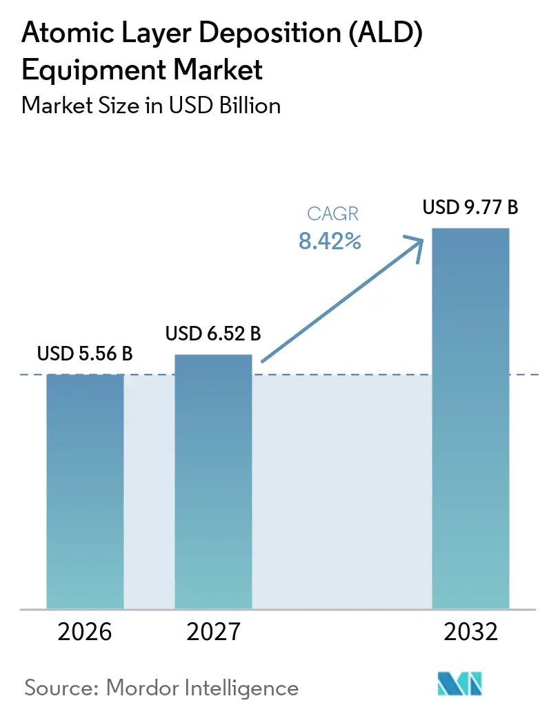
The global atomic layer deposition equipment market size is projected to expand from USD 5.56 billion in 2026 and USD 6.52 billion in 2027 to USD 9.77 billion by 2032, at a CAGR of 8.42% between 2027 and 2032. The market benefits from the growing number of deposition steps required in advanced logic and memory production. Atomic-scale control is increasingly important as chip designs move to smaller features and more complex structures. New fab projects in North America, Europe, and Japan are adding demand outside the established Asian manufacturing base. Suppliers are responding with integrated platforms, specialized chemistries, and service capacity that support customer qualification work. Supply constraints for specialized components and chemicals continue to lengthen delivery schedules and raise project costs.
Key Report Takeaways
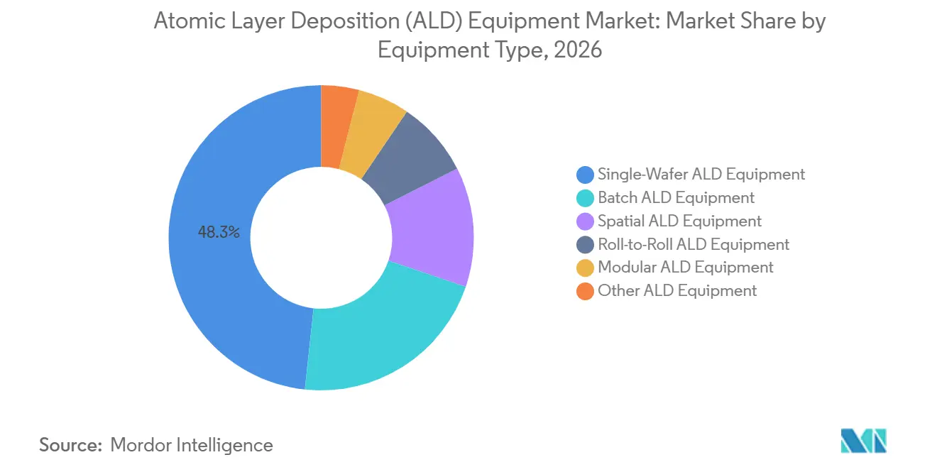
- By equipment type, single-wafer systems held 48.3% of the global ALD equipment market share in 2026, while spatial ALD equipment is forecast to grow at a CAGR of 8.7% through 2032.
- By technology, plasma-enhanced atomic layer deposition (PEALD) held 55.6% revenue share in 2026 and is forecast to grow at a CAGR of 8.8% through 2032.
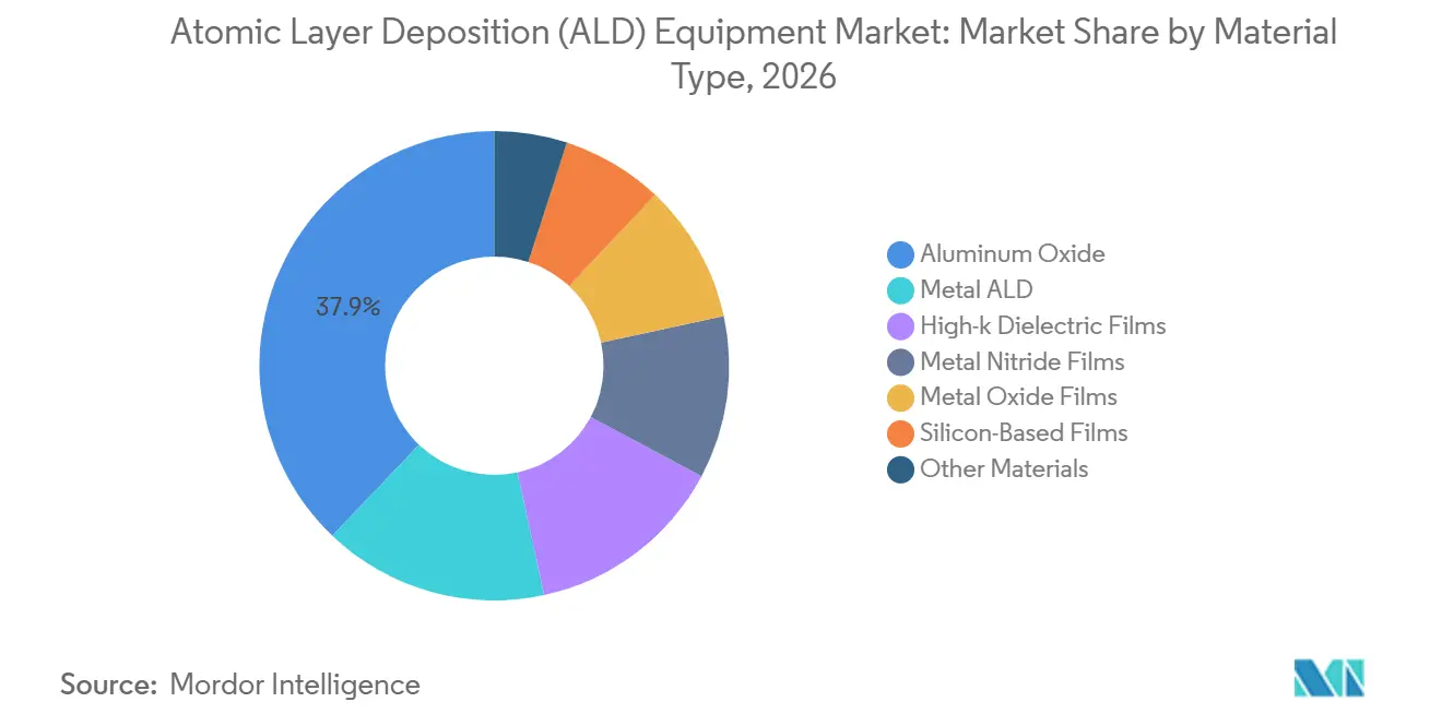
- By material type, aluminum oxide (Al2O3) held 37.9% revenue share in 2026, while metal nitride films are forecast to grow at a CAGR of 9.1% through 2032.
- By end-use industry, semiconductor manufacturing held 46.7% revenue share in 2026, while photovoltaics is forecast to grow at a CAGR of 9.7% through 2032.
- By geography, Asia-Pacific held 53.4% revenue share in 2026 and is forecast to grow at a CAGR of 8.9% through 2032.
Note: Market numbers in this report are based on Mordor Intelligence's proprietary estimation framework, which combines nine months of actuals with Q4 projections for base year 2026.
Market Trends and Insights
Drivers Impact Analysis of Atomic Layer Deposition (ALD) Equipment Market*
| Driver | (~) % Impact on CAGR Forecast | Geographic Relevance | Impact Timeline |
|---|---|---|---|
| Advanced-Node Logic and Memory Scaling | +2.0% | Global, led by Asia-Pacific, with growing North American demand | Long term (≥ 4 years) |
| 3D NAND and DRAM High-Aspect-Ratio Deposition | +1.5% | Asia-Pacific core, with spillover to North America | Long term (≥ 4 years) |
| GAA, High-k Metal-Gate and Selective Deposition Adoption | +1.3% | Global, especially Taiwan, South Korea, and the United States | Long term (≥ 4 years) |
| Advanced Packaging and Heterogeneous Integration | +1.0% | Global, especially Asia-Pacific and North America | Medium term (2-4 years) |
| Wide-Bandgap Power Electronics and Automotive Electrification | +0.6% | Europe, Asia-Pacific, and North America | Medium term (2-4 years) |
| Fab Localization and Government Semiconductor Incentives | +0.8% | North America, Europe, and Japan | Short term (≤ 2 years) |
| Source: Mordor Intelligence | |||
Advanced-Node Logic and Memory Scaling
Advanced logic at 2 nm and 3 nm requires more deposition steps than earlier FinFET generations. Film thickness tolerances have narrowed to single-digit angstroms, making repeatable layer control increasingly important. ASM International reported accelerating leading-edge demand, especially at the 2 nm node, and expected second-half 2026 revenue to exceed first-half revenue by more than 20% at constant currency.[1] The company also expected initial customer investments in 1.4 nm pilot lines during the second half of 2026. Each transition can add gate, barrier, and backside power-delivery layers rather than replace existing deposition steps. This creates demand that depends on process intensity per wafer as well as on wafer-start volumes.
GAA, High-k Metal-Gate and Selective Deposition Adoption
Gate-all-around structures use deposited dielectric and work-function metal layers around silicon nanosheets. Plasma-enhanced deposition can operate at lower temperatures, which helps preserve sensitive device structures. This requirement supports the global atomic layer deposition (ALD) equipment market where leading-edge process windows are narrow. Applied Materials Incorporated introduced its Endura Trillium platform to integrate several metal deposition steps in one vacuum cluster for angstrom-era logic.[2] The arrangement supports threshold-voltage tuning without vacuum breaks between stages. Applied Materials Incorporated also presented a plasma-based silicon nitride process for dense films in three-dimensional features. Area-selective deposition remains difficult to qualify because manufacturers need reliable measurement of selectivity at very small dimensions.
Advanced Packaging and Heterogeneous Integration
The global atomic layer deposition (ALD) equipment market is expanding its application base in advanced packaging. Chiplet assembly requires clean, uniform interfaces for fine-pitch bonding. An IEEE study reported void-free bonding between III-V and silicon substrates using ALD-deposited aluminum oxide (Al2O3) at temperatures below 250 °C, with bonding energy near 1.9 J/m² and shear strength above 25 MPa. In September 2026, Kokusai Electric Corporation and Yokohama National University reported that aluminum oxide (Al2O3) films enabled direct bonding on 300 mm wafers without plasma pretreatment. Capacity additions for front-end fabrication and packaging can therefore support separate equipment orders.
Fab Localization and Government Semiconductor Incentives
Government support is expanding the locations where new fab demand for the global atomic layer deposition (ALD) equipment market can emerge. The U.S. CHIPS program provides incentives for domestic semiconductor manufacturing and related supply chain investments. The CHIPS investment tax credit applies to eligible semiconductor manufacturing property, with projects required to begin construction by December 31, 2026 under the cited statutory provision. This policy environment can accelerate capital decisions at supported semiconductor sites. Multiple construction programs can place pressure on supplier engineering teams that must qualify tools at several new sites.
Restraints Impact Analysis of Atomic Layer Deposition (ALD) Equipment Market*
| Restraint | (~) % Impact on CAGR Forecast | Geographic Relevance | Impact Timeline |
|---|---|---|---|
| High Capital Cost and Total Cost of Ownership | -1.5% | Global, with greater pressure in emerging markets and mature-node fabs | Long term (≥ 4 years) |
| Throughput Gap Versus CVD and PVD | -1.0% | Global, especially mature-node and high-volume applications | Medium term (2-4 years) |
| Precursor Scarcity and Chemical-Utilization Economics | -0.7% | Global, especially for hafnium, molybdenum, and specialty organometallics | Medium term (2-4 years) |
| Area-Selective-Deposition Qualification and Metrology Bottlenecks | -0.4% | Global, mainly angstrom-era logic nodes | Long term (≥ 4 years) |
| Source: Mordor Intelligence | |||
High Capital Cost and Total Cost of Ownership
Single-wafer ALD chambers cost more than comparable CVD modules. The cost difference also includes precursor consumption, maintenance agreements, and the impact of tool downtime. Cost pressure is strongest in the ALD equipment market where mature-node applications do not require highly conformal films. Cost comparisons also depend on yield, required film quality, service response, and the number of processes steps a customer can consolidate. Smaller manufacturers may delay purchases when a lower-cost CVD process can meet device requirements. Restrictions on specialized subsystems can narrow the available supplier base and increase procurement risk. Tool builders with broad service organizations may be better positioned to support customers during long qualification programs.
Throughput Gap Versus CVD and PVD
ALD uses sequential precursor and purge stages, whereas CVD and PVD deposit material continuously. This makes ALD less attractive when throughput is more important than precise thickness control. A scientific paper described ALD as capable of producing pinhole-free films in high-aspect-ratio features while noting slower deposition rates than atmospheric CVD. Spatial configurations can improve throughput by separating reaction zones in space rather than in time. Beneq Transform markets spatial ALD tools for high-throughput photovoltaic and roll-to-roll coating applications.[3] Deep and narrow features still favor the conformality offered by ALD approaches, though the ALD equipment market retains a throughput constraint in some high-volume applications.
*Our forecasts treat driver/restraint impacts as directional, not additive. The impact forecasts reflect baseline growth, mix effects, and variable interactions.
Atomic Layer Deposition (ALD) Equipment Market Segment Analysis
By Equipment Type:
Single-Wafer Systems Support Advanced-Node ProductionSingle-wafer equipment held 48.3% of the Global atomic layer deposition (ALD) equipment market share in 2026. Foundry and logic customers use wafer-by-wafer processing where particle control and repeatability are critical. ASM described advanced logic and foundry as a central source of demand for its portfolio. The company targets more than 55% share in logic and foundry ALD through 2030. Batch systems serve memory and compound-semiconductor applications where throughput has greater weight. Roll-to-roll systems support flexible electronics and photovoltaic coatings.
Spatial ALD equipment is projected to grow at an 8.7% CAGR through 2032. This part of the Global atomic layer deposition (ALD) equipment market size benefits from applications that need faster coating across larger surfaces. A Royal Society of Chemistry study examined scalable nickel oxide deposition for inverted perovskite cells using ALD.[4] Fraunhofer reported a hybrid spatial ALD and PVD platform for electron-contact layers in perovskite-silicon tandem cells. Modular equipment is also gaining relevance in packaging flows that require several film chemistries on a shared platform. These architectures extend equipment demand into uses where conventional single-wafer systems are not the preferred cost option.

By Technology:
PEALD Serves Temperature-Sensitive and Three-Dimensional StructuresPEALD held 55.6% of technology revenue in 2026. Its position reflects demand from gate-all-around and stacked-memory production, where heat limits are tightly controlled. The Global atomic layer deposition (ALD) equipment market depends on technologies that can form uniform films without disrupting sensitive layers. Applied Materials introduced the Centris Spectral silicon nitride ALD platform in 2025 for dense films within three-dimensional structures. Its quad-reactor design is intended to improve uniformity in features with aspect ratios of 6:1 and above. Thermal ALD remains useful for aluminum oxide and hafnium oxide films when plasma-related interface damage must be avoided. Solar passivation, optical coatings, and selected memory dielectrics remain important applications.
Remote plasma and radical-assisted approaches are receiving interest where lower ion energy is needed. They can support flexible-substrate processing and deposition on two-dimensional materials. Spatial ALD is also developing as a distinct option for high-throughput uses. The Global atomic layer deposition (ALD) equipment market can therefore include multiple approaches within the same fab, with each tuned to a specific process step. The mix adds chamber demand as device structures become more complex. It also raises the importance of process integration and customer qualification work for equipment suppliers.
By Material Type:
Aluminum Oxide Leads While Metal Nitrides ExpandAluminum oxide held 37.9% of material-type revenue in 2026. It is used for silicon solar-cell passivation and insulation in GaN transistors, DRAM capacitors, and silicon-carbide MOSFETs. High-k dielectric films, led by hafnium oxide, are important for memory capacitors and logic gate dielectrics. Silicon-based and metal-oxide films serve specialty applications, including power-module passivation and photonic coatings. The Global atomic layer deposition (ALD) equipment market therefore serves both high-volume semiconductor structures and specialized thin-film requirements. Materials demand follows changes in device architecture, not only changes in total wafer production.
Metal nitride films are projected to grow at a 9.1% CAGR through 2032. Titanium nitride is used for DRAM capacitor electrodes, while aluminum nitride supports GaN device passivation. University of California research reported conformal titanium nitride ALD in test structures with aspect ratios of 2,000:1. Lam Research introduced ALTUS Halo for molybdenum metallization in 3D NAND, DRAM, and gate-all-around applications. Lam researchers also reported ALD molybdenum work for flash-memory wordline metallization. These materials illustrate why the Global atomic layer deposition (ALD) equipment market remains tied to the move toward taller and denser memory structures.
By End-Use Industry:
Semiconductor Manufacturing Remains Central as Photovoltaics Gains GroundSemiconductor manufacturing accounted for 46.7% of end-use demand in 2026. It uses ALD for gate dielectrics, barriers, spacers, liners, and metallization across logic and memory. The Global atomic layer deposition (ALD) equipment market is consequently exposed to both advanced-device investment and the timing of memory capacity expansion. The movement from FinFET to gate-all-around structures adds more process steps per wafer. Electronics manufacturing is the next important application group, including MEMS, capacitors, and display optical films. Industrial manufacturing and research settings support process development and specialized coating work. Aerospace and defense applications use precision coatings and can require specialized tool configurations.
Photovoltaics is projected to grow at a 9.7% CAGR through 2032. This part of the Global atomic layer deposition (ALD) equipment market size is supported by demand for passivation and encapsulation layers in TOPCon, HJT, and perovskite-silicon tandem cells. A Joule study reported a certified 26.59% power-conversion efficiency for a perovskite cell using an ALD-SnOx interface approach. Beneq reported qualification of its Transform cluster tool for 8-inch GaN-on-silicon power-device production in May 2025. Medical devices are an emerging application for ultra-thin biocompatible barriers on implants and biosensors. Those applications must meet the relevant manufacturing and validation requirements before broader adoption.
Geography Analysis
APAC Atomic Layer Deposition (ALD) Equipment Market
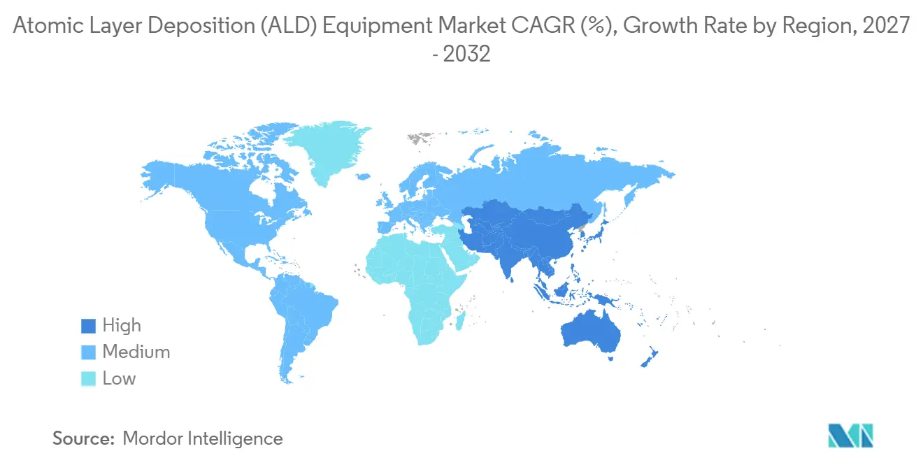
Asia-Pacific held a 53.4% revenue share in 2026 and is forecast to grow at an 8.9% CAGR through 2032. Taiwan, South Korea, China, and Japan collectively represent a large base of foundry, memory, and related electronics manufacturing. Samsung Electronics and SK Hynix are significant buyers of deposition systems for DRAM and 3D NAND production. Taiwan supports demand through Taiwan Semiconductor Manufacturing Company's investment in advanced nodes. Japan remains relevant for memory, logic, and batch-equipment applications. The concentration of advanced semiconductor production gives the region a durable demand base for process tools.
North America and Europe Atomic Layer Deposition (ALD) Equipment Market
North America is being shaped by new fab construction, tax incentives, and semiconductor supply chain investment. The CHIPS framework supports domestic semiconductor manufacturing and related investments. Intel Corporation's Ohio and Oregon projects also support equipment demand, while supplier capacity is needed for local qualification and service. Europe holds strategic importance through semiconductor and automotive power-device investment. The global atomic layer deposition (ALD) equipment market stands to benefit from these policy-backed regional projects as they progress from construction to equipment qualification. Chemical regulations may add qualification work for precursor alternatives, particularly where lower-toxicity or halide-free options are being considered.
The Americas and MEA Atomic Layer Deposition (ALD) Equipment Market
South America, the Middle East, and Africa account for a small share of equipment spending. Activity in these regions is concentrated in research centers, specialty coatings, and early-stage projects. Brazil and Mexico have limited industrial and R&D demand and face import-cost and local-supply constraints. The United Arab Emirates and Saudi Arabia are potential users of ALD-passivated thin-film photovoltaic modules within renewable energy projects. These regions present long-term opportunities rather than significant near-term equipment revenue. Their role in the global atomic layer deposition (ALD) equipment market depends on whether local manufacturing, specialist supply chains, and projects with sustained technical support develop further.
Competitive Landscape
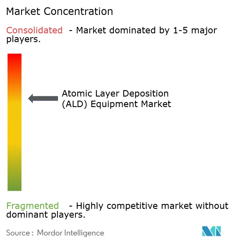
The global atomic layer deposition (ALD) equipment market is moderately concentrated in leading-edge logic and memory applications. ASM International, Tokyo Electron, Applied Materials, and Lam Research hold important qualification positions at major foundry and memory customers. ASM International targets more than 55% share in logic and foundry ALD through 2030. Its single-wafer platforms and service offerings are designed to retain a role through the operating life of qualified tools. Beneq, Oxford Instruments, Veeco, Wonik IPS, and Jusung Engineering compete in applications such as wide-bandgap devices, compound semiconductors, photovoltaics, and quantum technology, creating a more diverse competitive field outside the largest logic and memory fabs.
Leading suppliers are integrating more process steps within vacuum clusters. Applied Materials' Endura Trillium uses a clustered approach for gate-stack metal deposition. Lam Research launched ALTUS Halo for molybdenum ALD metallization, addressing the requirements of taller 3D NAND structures and advanced logic. Beneq introduced the Transmute platform in November 2025 for power, RF, and microLED production. These developments indicate that performance, throughput, and chemistry flexibility are competitive factors alongside installed-base relationships in the global ALD equipment market. Suppliers also require field engineering resources to support extended qualification work, recurring maintenance, and customer process changes.
Veeco raised its fiscal 2026 revenue guidance to USD 780 million to USD 810 million after reporting second-quarter revenue of USD 193.5 million. This reflects demand from memory, foundry logic, and EUV-related customers. Spatial ALD for tandem solar cells and deposition for quantum devices remain areas without a single dominant supplier. The global ALD equipment market combines concentrated leadership in advanced semiconductor production with niche competition in emerging applications. This structure gives established suppliers an advantage in high-volume qualification while leaving room for specialized providers in developing applications.
Atomic Layer Deposition (ALD) Equipment Industry Leaders
-
ASM International N.V.
-
Tokyo Electron Limited
-
Applied Materials, Inc.
-
Lam Research Corporation
-
Veeco Instruments Inc.
- *Disclaimer: Major Players sorted in no particular order
Atomic Layer Deposition (ALD) Equipment Market Companies Covered in this Report
- ASM International
- Tokyo Electron Limited
- Applied Materials, Inc.
- Lam Research Corporation
- Veeco Instruments Inc.
- Beneq Oy
- Picosun Oy
- Oxford Instruments plc
- Forge Nano Inc.
- CVD Equipment Corporation
- The Kurt J. Lesker Company
- Entegris, Inc.
- SENTECH Instruments GmbH
- Aixtron SE
- Nano-Master, Inc.
- Arradiance, LLC
- NCD Co., Ltd.
- Wonik IPS Co., Ltd.
- Jusung Engineering Co., Ltd.
- NAURA Technology Group Co., Ltd.
- ULVAC, Inc.
Recent Industry Developments in Atomic Layer Deposition (ALD) Equipment Market
- September 2026: Kokusai Electric, in collaboration with Yokohama National University and supported by the Japan Science and Technology Agency (JST) A-STEP funding, announced research demonstrating that ALD Al₂O₃ films enable self-activated direct bonding on 300 mm wafers without plasma pre-treatment. This development removes a key process step in chiplet packaging and 3D heterogeneous integration, potentially simplifying advanced semiconductor manufacturing workflows.
- August 2026: Veeco Instruments reported revenue of USD 193.5 million, up 22% sequentially, with semiconductor revenue increasing 20% quarter-over-quarter. The company raised its full-year 2026 revenue guidance to USD 780 million to USD 810 million, citing strong demand from memory, foundry/logic, advanced packaging, and EUV-related applications that increasingly rely on deposition technologies including ALD.
- November 2025: Beneq introduced the Transmute platform, a high-volume manufacturing ALD system designed for wide-bandgap power semiconductors, RF devices, and microLED production. The system integrates plasma pretreatment, plasma-enhanced ALD (PEALD), and thermal batch ALD capabilities within a single production platform, targeting high-throughput industrial manufacturing environments.
- February 2025: Lam Research unveiled ALTUS Halo, an ALD system engineered for molybdenum metallization in advanced semiconductor applications. The platform addresses requirements in 3D NAND wordlines, DRAM, and gate-all-around (GAA) transistor structures, where molybdenum is increasingly replacing traditional tungsten-based processes.
Global Atomic Layer Deposition (ALD) Equipment Market Report Scope
Atomic Layer Deposition (ALD) equipment refers to specialized semiconductor manufacturing machinery used to deposit ultra-thin, highly uniform material layers onto substrates with atomic-scale precision. The equipment operates through a self-limiting, sequential gaseous process, introducing chemical precursors one at a time to react with the surface sequentially. This cyclical process ensures precise film thickness control and conformal coating, even over complex, high-aspect-ratio 3D microstructures. As a result, ALD systems are widely used in the fabrication of advanced microelectronics, logic chips, memory devices, and nanotechnology applications.
The global Atomic Layer Deposition (ALD) Equipment Market is segmented by equipment type into single-wafer ALD equipment, batch ALD equipment, spatial ALD equipment, roll-to-roll ALD equipment, modular ALD equipment, and other ALD equipment. By technology, the market is segmented into thermal ALD, plasma-enhanced ALD (PEALD), spatial ALD, remote plasma ALD, radical-assisted ALD, and other ALD technologies. By material type, the market is segmented into aluminum oxide (Al2O3), metal ALD, high-k dielectric films, metal nitride films, metal oxide films, silicon-based films, and other materials. By end-use industry, the market is segmented into semiconductor manufacturing, electronics manufacturing, energy and power, photovoltaics, automotive, aerospace and defense, healthcare and medical, research and development, industrial manufacturing, and other industries. The report also covers the market size and forecasts for the global ALD equipment market across 26 countries in key regions. For each segment, the market sizing and forecasts are provided on the basis of value (USD).
Segmentation Overview
| Single-Wafer ALD Equipment |
| Batch ALD Equipment |
| Spatial ALD Equipment |
| Roll-to-Roll ALD Equipment |
| Modular ALD Equipment |
| Other ALD Equipment |
| Thermal ALD |
| Plasma-Enhanced ALD (PEALD) |
| Spatial ALD |
| Remote Plasma ALD |
| Radical-Assisted ALD |
| Other ALD Technologies |
| Aluminum Oxide (Al₂O₃) |
| Metal ALD |
| High-k Dielectric Films |
| Metal Nitride Films |
| Metal Oxide Films |
| Silicon-Based Films |
| Other Materials |
| Semiconductor Manufacturing |
| Electronics Manufacturing |
| Energy and Power |
| Photovoltaics |
| Automotive |
| Aerospace and Defense |
| Healthcare and Medical |
| Research and Development |
| Industrial Manufacturing |
| Other Industries |
| North America | United States |
| Canada | |
| Mexico | |
| Europe | Germany |
| France | |
| Italy | |
| Spain | |
| United Kingdom | |
| Poland | |
| Russia | |
| Rest of Europe | |
| Asia-Pacific | China |
| India | |
| Japan | |
| South Korea | |
| Australia | |
| Indonesia | |
| Vietnam | |
| Thailand | |
| Rest of Asia-Pacific | |
| South America | Brazil |
| Argentina | |
| Chile | |
| Rest of South America | |
| Middle East and Africa | Saudi Arabia |
| United Arab Emirates | |
| Egypt | |
| South Africa | |
| Morocco | |
| Rest of Middle East and Africa |
| By Equipment Type | Single-Wafer ALD Equipment | |
| Batch ALD Equipment | ||
| Spatial ALD Equipment | ||
| Roll-to-Roll ALD Equipment | ||
| Modular ALD Equipment | ||
| Other ALD Equipment | ||
| By Technology | Thermal ALD | |
| Plasma-Enhanced ALD (PEALD) | ||
| Spatial ALD | ||
| Remote Plasma ALD | ||
| Radical-Assisted ALD | ||
| Other ALD Technologies | ||
| By Material Type | Aluminum Oxide (Al₂O₃) | |
| Metal ALD | ||
| High-k Dielectric Films | ||
| Metal Nitride Films | ||
| Metal Oxide Films | ||
| Silicon-Based Films | ||
| Other Materials | ||
| By End-Use Industry | Semiconductor Manufacturing | |
| Electronics Manufacturing | ||
| Energy and Power | ||
| Photovoltaics | ||
| Automotive | ||
| Aerospace and Defense | ||
| Healthcare and Medical | ||
| Research and Development | ||
| Industrial Manufacturing | ||
| Other Industries | ||
| By Geography | North America | United States |
| Canada | ||
| Mexico | ||
| Europe | Germany | |
| France | ||
| Italy | ||
| Spain | ||
| United Kingdom | ||
| Poland | ||
| Russia | ||
| Rest of Europe | ||
| Asia-Pacific | China | |
| India | ||
| Japan | ||
| South Korea | ||
| Australia | ||
| Indonesia | ||
| Vietnam | ||
| Thailand | ||
| Rest of Asia-Pacific | ||
| South America | Brazil | |
| Argentina | ||
| Chile | ||
| Rest of South America | ||
| Middle East and Africa | Saudi Arabia | |
| United Arab Emirates | ||
| Egypt | ||
| South Africa | ||
| Morocco | ||
| Rest of Middle East and Africa | ||
Key Questions Answered in the Report
What is driving demand for atomic layer deposition equipment?
Demand is supported by advanced logic and memory production, where tighter device structures require highly controlled thin films.
How large is the global atomic layer deposition equipment market in 2027?
The market is estimated at USD 6.52 billion in 2027 and is forecast to reach USD 9.77 billion by 2032, at a CAGR of 8.42%.
Which equipment architecture leads atomic layer deposition demand?
Single-wafer equipment held a 48.3% share in 2026, as advanced logic and foundry production require strong particle control.
Why is plasma-enhanced atomic layer deposition important for semiconductor fabrication?
Plasma-enhanced atomic layer deposition accounted for 55.6% of technology revenue in 2026, as it supports temperature-sensitive, three-dimensional device structures.
Which end-use application is growing fastest for atomic layer deposition tools?
Photovoltaics is projected to grow at a CAGR of 9.7% through 2032, as advanced solar architectures adopt atomic layer deposition passivation and encapsulation layers.
Which region leads equipment demand?
Asia-Pacific held a 53.4% share in 2026 and is projected to grow at a CAGR of 8.9% through 2032.