
EUV Pellicle Market Size and Share
Market Overview
| Study Period | 2021 - 2031 |
|---|---|
| Market Size (2026) | USD 0.85 Billion |
| Market Size (2031) | USD 1.60 Billion |
| Growth Rate (2026 - 2031) | 13.47 % |
| Fastest Growing Market | Asia-Pacific |
| Largest Market | Asia-Pacific |
| Market Concentration | High |
Major Players *Disclaimer: Major Players sorted in no particular order Image © Mordor Intelligence. Reuse requires attribution under CC BY 4.0. | |
EUV Pellicle Market Analysis by Mordor Intelligence
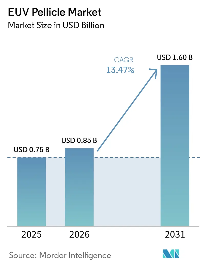
The EUV Pellicle Market size was valued at USD 0.75 billion in 2025 and is estimated to grow from USD 0.85 billion in 2026 to reach USD 1.60 billion by 2031, at a CAGR of 13.47% during the forecast period (2026-2031). The move to advanced logic nodes is increasing the number of Extreme Ultraviolet (EUV) exposures required for each wafer. Taiwan Semiconductor Manufacturing Company Limited began production of its 2 nm technology in Q4 2025, and its A16 technology is production-ready in 2H 2026, which extends demand for qualified pellicles across successive node transitions. Demand for artificial intelligence, high-performance computing, and advanced logic is raising the value placed on stable exposure processes and mask protection. High-Numerical Aperture (NA) EUV systems are also increasing the need for membranes that retain high transmittance at greater source power. Suppliers that can qualify durable materials, add manufacturing capacity, and support customers through long validation cycles have a stronger position in the EUV pellicle market.
Key Report Takeaways
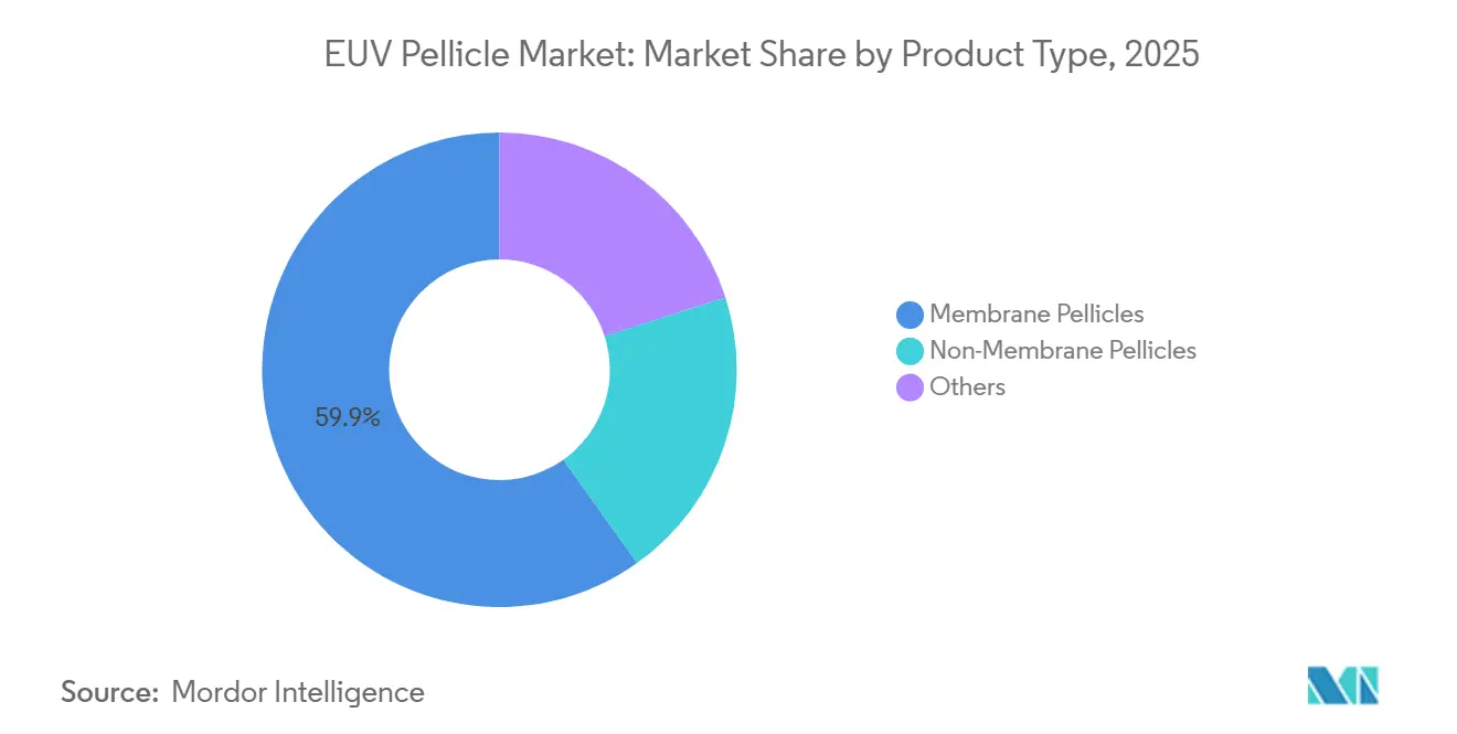
- By product type, membrane pellicles held a 59.85% of the EUV pellicle market share in 2025, while non-membrane pellicles are projected to advance at a 14.74% CAGR through 2031.
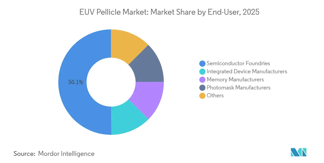
- By end-user, semiconductor foundries held 50.12% of the EUV pellicle market share in 2025, while memory manufacturers are projected to advance at a 15.66% CAGR through 2031.
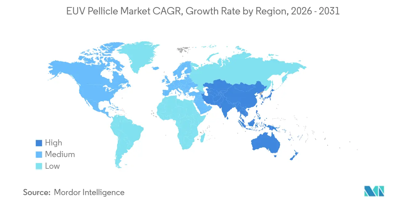
- By geography, Asia-Pacific held 62.78% of the EUV pellicle market share in 2025 and is projected to advance at a 14.31% CAGR through 2031.
Note: Market size and forecast figures in this report are generated using Mordor Intelligence’s proprietary estimation framework, updated with the latest available data and insights as of January 2026.
Market Trends and Insights
Drivers Impact Analysis of EUV Pellicle Market*
| Driver | (~) % Impact on CAGR Forecast | Geographic Relevance | Impact Timeline |
|---|---|---|---|
| Expansion of EUV Lithography in 5 nm, 3 nm and 2 nm Production | +3.2% | Global, concentrated in APAC (Taiwan, South Korea, Japan) | Short term (≤ 2 years) |
| Rising AI, High-Performance Computing and Advanced Logic Demand | +2.8% | Global, demand originating in North America and China, capacity in APAC | Short term (≤ 2 years) |
| High-NA EUV Adoption Requiring Higher-Transmittance Pellicles | +2.2% | APAC (South Korea, Japan); early spillover to North America | Medium term (2-4 years) |
| Increasing EUV Layer Counts in DRAM and NAND Manufacturing | +1.9% | APAC core (South Korea, Japan, Taiwan) | Medium term (2-4 years) |
| Higher EUV Source Power Increasing Pellicle Replacement Requirements | +1.4% | Global, aligned to ASML scanner installed base locations | Long term (≥ 4 years) |
| Source: Mordor Intelligence | |||
Expansion of EUV Lithography in 5 nm, 3 nm and 2 nm Production
Each successive logic node requires more EUV patterning steps than its predecessor, increasing recurring use requirements in the EUV pellicle market. This creates a direct increase in exposure activity and pellicle use per wafer across logic production, which gives the EUV pellicle market a demand base. Taiwan Semiconductor Manufacturing Company Limited placed its 2 nm technology into production in Q4 2025 with nanosheet transistors that require tighter overlay control than 3 nm FinFET production. The company’s A16 technology is production-ready in 2H 2026 and is intended for high-performance computing and artificial intelligence applications. Existing 5 nm equipment can also be adapted to add 3 nm capacity over a 6-to-12-month cycle, which creates further demand because the newer process uses more EUV patterning steps and tighter process tolerances. Samsung’s Taylor, Texas, facility, which targets advanced-node production, adds a North American location for this demand.
Rising AI, High-Performance Computing and Advanced Logic Demand
Artificial intelligence infrastructure supports sustained investment in leading-edge semiconductor capacity and supports more consistent utilization across the EUV pellicle market. Advanced processors carry a high value per wafer, which increases the importance of avoiding interruptions caused by mask contamination and makes proven pellicle protection more operationally relevant for high-throughput fabs. ASML stated in its Q2 2026 results that it is expanding EUV capacity for 2027 in response to demand linked to artificial intelligence infrastructure. This demand comes from customers including TSMC, Samsung, and Intel, whose advanced-node capacity plans influence the EUV pellicle market across the wider materials supply chain. It supports continued use of established membrane materials while newer carbon nanotube (CNT) materials move through qualification. It also gives pellicle suppliers an incentive to improve productivity because higher scanner availability can translate into more advanced-chip output.
High-NA EUV Adoption Requiring Higher-Transmittance Pellicles
High numerical aperture, or High-NA, EUV lithography operates at 0.55 numerical aperture rather than 0.33 numerical aperture for conventional EUV systems. This creates a distinct technical transition for the EUV pellicle market. ASML states that its EXE:5200B can print features 1.7 times finer than current EUV tools and achieve 2.9 times higher transistor densities. This raises requirements for pellicle heat resistance, mechanical stability, and transmittance, as source-power roadmaps move from the 380 W range toward 600 W and eventually 1,000 W. Research presented through SPIE described the challenge of developing pellicles that can support 1,000 W EUV source power. CNT membranes have demonstrated 95% to 98% transmittance, limiting the dose increase to 4% to 9%, and can withstand temperatures above 1,500 °C in reported exposure results. The EUV pellicle market, therefore, favors suppliers that can convert laboratory performance into qualified, repeatable production material.
Higher EUV Source Power Increasing Pellicle Replacement Requirements
Higher source power places added thermal requirements on the EUV pellicle market and added thermal and chemical stress on pellicle membranes during extended exposure cycles in hydrogen plasma environments. The need to preserve optical transmission becomes more important as scanner output rises, because a loss in transmittance can increase dose requirements and affect scanner productivity. Silicon-based composite pellicles can operate in established low-NA applications, but higher power requires stronger performance margins. CNT pellicles are being developed to address this need because their material structure can combine high transmittance with thermal resilience. Mitsui Chemicals, Inc. established CNT pellicle facilities at Iwakuni-Ohtake Works with planned compatibility for EUV source powers above 1 kW[1]. More demanding source-power conditions may also shorten effective pellicle life, supporting replacement demand when products complete qualification.
Restraints Impact Analysis of EUV Pellicle Market*
| Restraint | (~) % Impact on CAGR Forecast | Geographic Relevance | Impact Timeline |
|---|---|---|---|
| Stringent Defectivity, Lifetime and Uniformity Qualification | -1.8% | Global; most acute at TSMC (Taiwan), Samsung and SK hynix (South Korea) fabs operating at leading nodes | Short term (≤ 2 years) |
| High Pellicle Cost Relative to Conventional DUV Alternatives | -1.3% | Global, with higher sensitivity in cost-constrained foundries in China and emerging markets | Medium term (2-4 years) |
| Limited Qualified Supplier and Manufacturing Base | -0.9% | Global supply-side constraint; geographic concentration risk in Japan and South Korea | Long term (≥ 4 years) |
| Source: Mordor Intelligence | |||
Stringent Defectivity, Lifetime and Uniformity Qualification
EUV pellicles face a demanding qualification process that governs entry into the EUV pellicle market, which limits the speed of supplier entry. Membranes that are 30 to 50 nm thick must maintain transmittance uniformity within a half-range of 0.4% across a 110 mm × 144 mm area. They must also survive 20,000 or more wafer exposures in hydrogen plasma conditions. Hydrogen exposure can gradually reduce optical transmission and embrittle the membrane after thousands of exposures, which makes lifetime prediction a production-critical engineering requirement. The challenge affects both CNT and silicon-based materials, as durability work on metal-silicide pellicles has shown. Production also requires cleanroom controls and particle limits that restrict the number of facilities able to support qualified output, including the ISO 14644 Class 1 conditions used in this manufacturing workflow.
High Pellicle Cost Relative to Conventional DUV Alternatives
EUV pellicles in the EUV pellicle market cost more than conventional deep ultraviolet (DUV) pellicles. The difference affects per-wafer economics, especially at mature EUV nodes where margins can be tighter and the immediate productivity benefit must be weighed against consumable spending. Some fabs may operate without a pellicle when they judge the contamination risk to be acceptable. This approach trades lower consumable spending for a greater risk of mask-related interruptions. An ASML paper reported that a new EUV pellicle can improve scanner productivity by more than 20% compared with operation without a pellicle. Adoption of new materials will depend on both proven technical performance and a credible path to lower production costs.
*Our forecasts treat driver/restraint impacts as directional, not additive. The impact forecasts reflect baseline growth, mix effects, and variable interactions.
EUV Pellicle Market Segment Analysis
By Product Type:
Membrane Pellicles Lead While Non-Membrane Pellicles Support GrowthMembrane pellicles held a 59.85% share of the EUV pellicle market in 2025. Their position was supported by the installed base of ASML NXE 0.33 NA scanners operating at source powers up to 400 W. Silicon-based and metal-silicide composite membranes have accumulated production exposure data at TSMC, Samsung, and SK hynix fabs. That operating history remains important because customers require extensive evidence before approving another pellicle material. Their established compatibility with scanner, mask, and reticle-handling processes supports continued demand, while the EUV pellicle industry depends on material consistency as much as laboratory transmittance.
Non-membrane pellicles in the EUV pellicle market are projected to advance at a 14.74% CAGR through 2031. This category includes CNT membrane pellicles and other non-patterned protection approaches. CANATU’s Floating Catalyst Chemical Vapor Deposition (FC-CVD) CNT reactor technology is licensed to FST, while Mitsui Chemicals, Inc. is building its own CNT pellicle capability. Other commercially early approaches include photomask-integrated protection concepts and experimental materials, while metal-silicide composites demonstrate more than 90% transmittance and survival through 20,000 wafer exposures at 400 W in controlled testing. Both established composites and CNT options are, therefore, likely to remain relevant through 2031.

By End-User:
Semiconductor Foundries Lead, While Memory Manufacturers AccelerateSemiconductor foundries held a 50.12% share of the EUV pellicle market in 2025. Their demand is concentrated among TSMC, Samsung Foundry, Intel Foundry, and a small number of specialized fabs. In 2025, 5 manufacturers operated EUV in high-volume production: TSMC, Samsung, Intel, SK hynix, and Micron. This concentrated customer base gives qualified pellicle suppliers direct visibility into demand changes, but qualification decisions remain highly consequential because advanced logic capacity needs stable mask protection during complex exposure steps. Foundries also apply distinct qualification requirements, which makes customer support and process knowledge important.
Memory manufacturers in the EUV pellicle market are projected to advance at a 15.66% CAGR through 2031. Higher EUV layer counts in Dynamic Random-Access Memory (DRAM) and Micron’s initial EUV use at its 1-gamma Hiroshima facility are supporting this increase. ASML confirmed in Q1 2026 that memory customers were progressing High-NA systems toward mass production. Photomask manufacturers use pellicles mainly for mask qualification and inspection. Dai Nippon Printing, HOYA, and Toppan serve this value chain, while research institutions and pilot lines create episodic demand linked to qualification projects. Memory-related demand is supported by new device generations and rising process intensity.
Geography Analysis
APAC EUV Pellicle Market
Asia-Pacific held 62.78% of the EUV pellicle market share in 2025 and is projected to advance at a 14.31% CAGR through 2031. The region hosts the major EUV-capable chipmakers and much of the related materials supply chain, so installed scanner capacity and qualified membrane production are closely linked geographically. South Korea is a major demand center because Samsung and SK Hynix operate leading logic and memory fabs. Taiwan is central to foundry consumption because TSMC is ramping multiple 2 nm fabs.
East and South Asia EUV Pellicle Market
Japan combines local demand with supply from Mitsui Chemicals and Shin-Etsu Chemical, while China’s EUV pellicle market demand remains constrained by export controls on EUV scanner shipments. Domestic chipmakers are expanding DUV capacity, which can support related pellicle demand through photomask operations. India, ASEAN countries, and the rest of the Asia-Pacific region remain at earlier stages of advanced semiconductor investment. India’s semiconductor incentive program is attracting downstream assembly capacity that may become a future demand signal if the regional manufacturing base moves further into wafer fabrication.
The Americas and EMEA EUV Pellicle Market
North America’s demand is supported by announced logic and memory investments that widen its role in advanced semiconductor manufacturing. Intel’s EUV-enabled fabs in Oregon and Arizona, Samsung’s Taylor facility, and Micron’s U.S. expansion support regional demand. U.S. primary membrane supply is limited, while Entegris provides reticle-handling and contamination-control infrastructure. Europe has a strategic role because ASML is based in the Netherlands and Carl Zeiss SMT produces optical columns in Germany, while South America and Middle East and Africa have low demand because neither region operates EUV-capable fabs. Saudi Arabia’s chip investment plans remain focused on packaging and design rather than leading-edge wafer fabrication in the near term.
Competitive Landscape
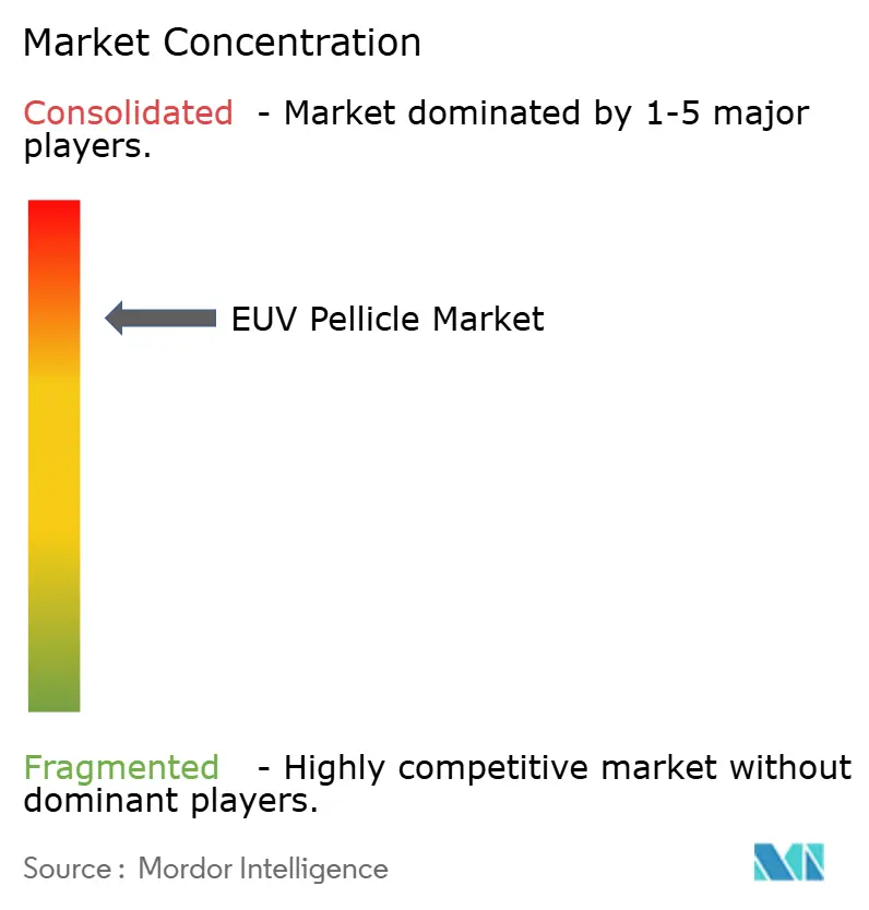
The EUV pellicle market is consolidated, with the top five players including Mitsui Chemicals, Inc., ASML, S & S Technologies, FST, and CANATU. The position reflects technical barriers between a working prototype and a production-qualified consumable. ASML has a distinct role as the sole EUV scanner manufacturer and as the company that defines pellicle qualification specifications. Mitsui Chemicals, Inc. holds a pellicle production license from ASML and has sold pellicles commercially since 2021.
S & S Technologies, FST, and Entegris compete across the EUV pellicle market in frame, assembly, mask protection, and reticle pod integration. CNT manufacturing scale is a central competitive area through 2031, as suppliers seek to translate higher-transmittance performance into dependable commercial output. CANATU licensed its FC-CVD reactor technology to FST in October 2025 under a commercial production framework. In August 2026, CANATU received a second CNT100 SEMI reactor order from FST, which is scheduled for delivery in 2027. Mitsui Chemicals, Inc. is pursuing a separate CNT route through its work with imec and its Iwakuni-Ohtake production facilities.
Sumitomo Chemical Co., Ltd. and SKC are advancing their own membrane chemistries, while FUJIFILM Group has capabilities in precision coating and nanomaterial deposition. Shin-Etsu Chemical Co., Ltd. has protected EUV pellicle frame configurations through a European patent covering thermal-expansion compensation[2]. FST’s use of CANATU’s reactor approach offers another path to supply growth, but suppliers must meet ISO 14644 Class 1 cleanroom requirements and SEMI particle-adder guidelines. These requirements favor companies that can demonstrate process control in qualified manufacturing environments and maintain stable quality through each stage of assembly.
EUV Pellicle Industry Leaders
-
Mitsui Chemicals, Inc.
-
ASML
-
S & S Technologies
-
CANATU
-
FST
- *Disclaimer: Major Players sorted in no particular order
EUV Pellicle Market Companies Covered in this Report
- AGC Inc.
- ASML
- CANATU
- Dai Nippon Printing Co., Ltd.
- Entegris
- FST
- FUJIFILM Group
- HOYA Corporation
- Mitsui Chemicals, Inc.
- S & S Technologies
- Shin-Etsu Chemical Co., Ltd.
- SKC Co., Ltd.
- Sumitomo Chemical Co., Ltd.
- Toppan Inc.
Recent Industry Developments in EUV Pellicle Market
- August 2026: CANATU secured an order from Fine Semitech Corporation for a second CNT100 SEMI reactor to expand carbon nanotube pellicle manufacturing capacity. The investment supported the scale-up of CNT pellicle production for EUV lithography, where pellicles protect photomasks while maintaining high EUV transmission.
- February 2026: LINTEC Corporation developed a new coating formulation designed to significantly improve the durability of carbon nanotube pellicles used in EUV lithography. Through joint research with the National Institute of Advanced Industrial Science and Technology (AIST), LINTEC Corporation advanced mass-production technologies for CNT pellicles, supporting the development of more durable and reliable pellicles for advanced semiconductor patterning.
Global EUV Pellicle Market Report Scope
EUV pellicles are ultra-thin protective layers used to shield photomasks from particle contamination during extreme ultraviolet lithography. They help protect mask patterns and support consistent wafer patterning during advanced semiconductor manufacturing.
The EUV Pellicle Market is segmented by product type, end-user, and geography. By product type, the market is segmented into membrane pellicles, non-membrane pellicles, and others. By end-user, the market is segmented into semiconductor foundries, integrated device manufacturers, memory manufacturers, photomask manufacturers, and others. The report also covers the market size and forecasts for EUV pellicles in 15 countries across major regions. For each segment, the market sizing and forecasts have been done on the basis of value (USD).
Segmentation Overview
| Membrane Pellicles |
| Non-Membrane Pellicles |
| Others |
| Semiconductor Foundries |
| Integrated Device Manufacturers |
| Memory Manufacturers |
| Photomask Manufacturers |
| Others |
| Asia-Pacific | China |
| India | |
| Japan | |
| South Korea | |
| ASEAN Countries | |
| Rest of Asia-Pacific | |
| North America | United States |
| Canada | |
| Mexico | |
| Europe | Germany |
| United Kingdom | |
| France | |
| Italy | |
| NORDIC Countries | |
| Rest of Europe | |
| South America | Brazil |
| Argentina | |
| Rest of South America | |
| Middle East and Africa | Saudi Arabia |
| South Africa | |
| Rest of Middle East and Africa |
| By Product Type | Membrane Pellicles | |
| Non-Membrane Pellicles | ||
| Others | ||
| By End-User | Semiconductor Foundries | |
| Integrated Device Manufacturers | ||
| Memory Manufacturers | ||
| Photomask Manufacturers | ||
| Others | ||
| By Geography | Asia-Pacific | China |
| India | ||
| Japan | ||
| South Korea | ||
| ASEAN Countries | ||
| Rest of Asia-Pacific | ||
| North America | United States | |
| Canada | ||
| Mexico | ||
| Europe | Germany | |
| United Kingdom | ||
| France | ||
| Italy | ||
| NORDIC Countries | ||
| Rest of Europe | ||
| South America | Brazil | |
| Argentina | ||
| Rest of South America | ||
| Middle East and Africa | Saudi Arabia | |
| South Africa | ||
| Rest of Middle East and Africa | ||
Key Questions Answered in the Report
What is the size of the EUV pellicle market?
The EUV pellicle market stands at USD 0.85 billion in 2026 and is projected to reach USD 1.60 billion by 2031.
What is driving demand for EUV pellicles?
Growth in 2 nm, 3 nm, and 5 nm production, artificial intelligence processors, and high-performance computing is increasing EUV exposure activity. Higher EUV layer counts in DRAM and NAND flash also support demand.
Which product type led market demand in 2025?
Membrane pellicles held a 59.85% of the demand in 2025 because they were qualified for the installed base of conventional EUV scanners.
Why are CNT pellicles important?
CNT pellicles have reported 95% to 98% EUV transmittance and are being developed for higher-power and High-NA EUV tools. Their expected role depends on completing the long qualification process required for production fabs.