
Size and Share of Asia-Pacific Solder Materials Market In Semiconductor Industry
Market Overview
| Study Period | 2021 - 2032 |
|---|---|
| Forecast Data Period | 2027 - 2032 |
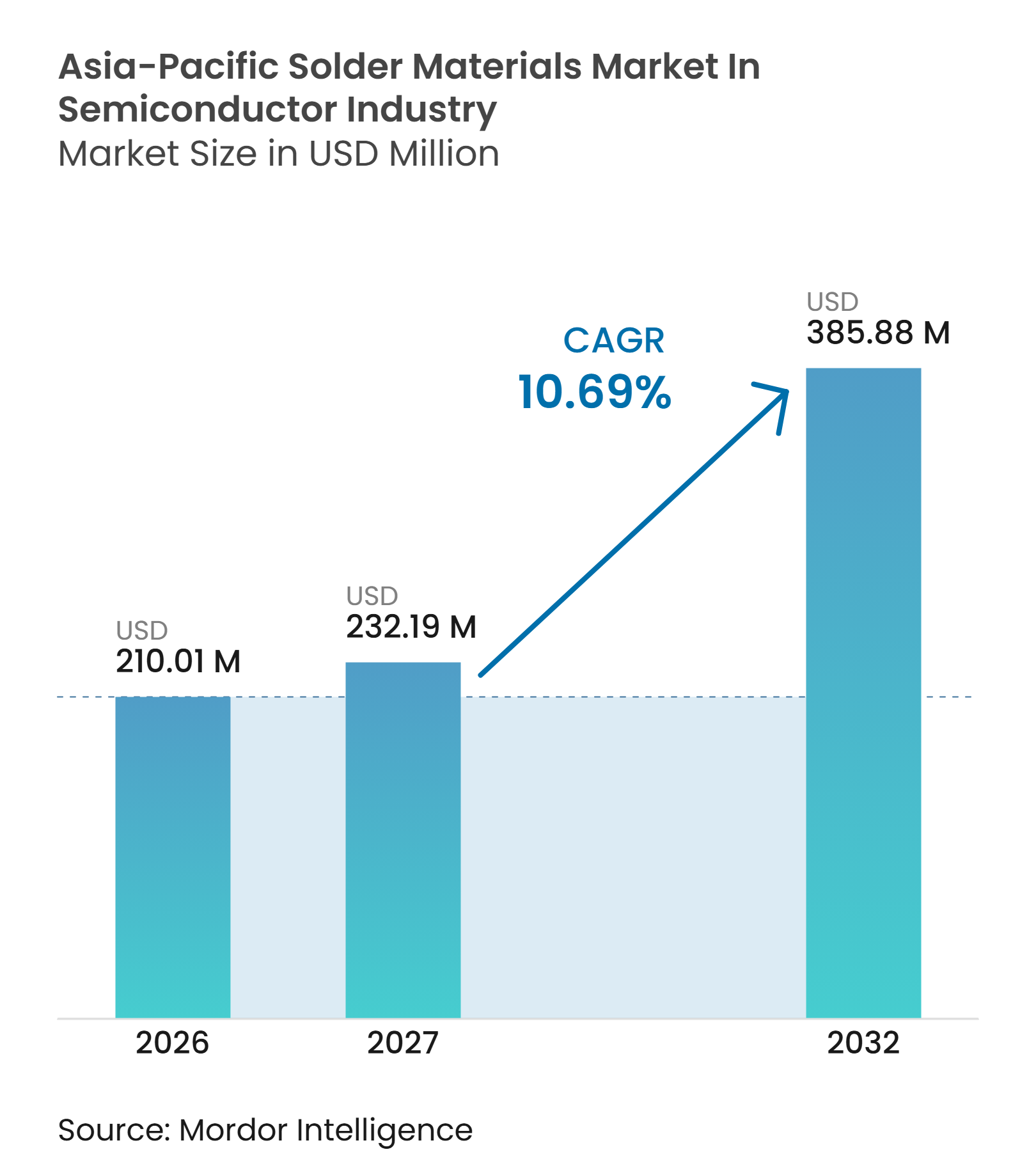
| Base Year Market Size (2026) | USD 210.01 Million |
| Market Size (2027) | USD 232.19 Million |
| Market Size (2032) | USD 385.88 Million |
| Growth Rate (2027 - 2032) | 10.69 % |
| Market Concentration | Medium |
Major Players *Disclaimer: Major Players sorted in no particular order Image © Mordor Intelligence. Reuse requires attribution under CC BY 4.0. | |
Analysis of Asia-Pacific Solder Materials Market In Semiconductor Industry by Mordor Intelligence
The Asia-Pacific solder materials market in semiconductor industry size is valued at USD 210.01 million in 2026 and is projected to reach USD 385.88 million by 2032, registering a CAGR of 10.69% from 2027 to 2032. Demand is shifting toward application-specific alloys because heterogeneous integration needs consistent metallurgy across high-volume advanced packaging lines. AI accelerators, high-bandwidth memory stacks, and chiplet packages require finer solder balls, tighter diameter control, and lower void rates than conventional semiconductor packages. China remains the largest country market, supported by its concentration of wafer fabrication, outsourced semiconductor assembly and test capacity, substrate manufacturing, and electronics production. India and Southeast Asia are adding new packaging capacity, which broadens the regional qualification base for solder paste, microballs, preforms, and related materials. Competition is strongest in premium materials, where patent positions, controlled atomization, technical support, and approved qualification records remain important barriers.
Key Report Takeaways
- By product form, solder paste held 31.82% of the Asia-Pacific solder materials market in semiconductor industry market share in 2026, while solder balls and spheres are projected to expand at a CAGR of 10.82% through 2032.
- By applicable market, logic ICs held 32.63% regional share in 2026, while memory ICs are projected to expand at a CAGR of 10.97% through 2032.
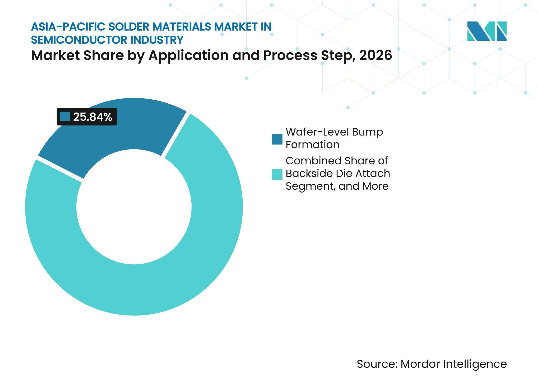
- By application and process step, wafer-level bump formation accounted for 25.84% of the Asia-Pacific solder materials market in semiconductor industry market size in 2026 and is projected to expand at a CAGR of 11.08% through 2032.
- By geography, China held 32.38% of the Asia-Pacific solder materials market in semiconductor industry market share in 2026, while India is projected to expand at a CAGR of 11.23% through 2032.
Note: Market numbers in this report are based on Mordor Intelligence's proprietary estimation framework, which combines nine months of actuals with Q4 projections for base year 2026.
Market Trends and Insights
Drivers Impact Analysis of Asia-Pacific Solder Materials Market In Semiconductor Industry*
| Driver | (~) % Impact on CAGR Forecast | Geographic Relevance | Impact Timeline |
|---|---|---|---|
| Advanced Packaging for AI, HBM, and Chiplet Architectures | +3.5% | Global, highest intensity in Taiwan, South Korea, and China | Medium term (2-4 years) |
| Expansion of Semiconductor and OSAT Capacity in Asia-Pacific | +2.5% | Asia-Pacific core, China, Taiwan, and South Korea, with spillover to India, Malaysia, and Vietnam | Medium term (2-4 years) |
| Lead-Free Conversion and Hazardous-Substance Restrictions | +1.5% | Global, with early compliance pressure in China, Japan, and South Korea | Short term (≤ 2 years) |
| Automotive Electrification and High-Reliability Power Electronics | +1.2% | Asia-Pacific core, China, Japan, and South Korea, with spillover to India | Medium term (2-4 years) |
| India and Southeast Asia Packaging Localization | +1.0% | India, Malaysia, Vietnam, Thailand, and Singapore | Long term (≥ 4 years) |
| Fine-Pitch Miniaturization and Low-Temperature Interconnects | +0.8% | Taiwan, South Korea, and Japan | Medium term (2-4 years) |
| Source: Mordor Intelligence | |||
Advanced Packaging for AI, HBM, and Chiplet Architectures
The move toward heterogeneous integration is changing both the volume and performance requirements for solder materials across Asia-Pacific semiconductor lines. AI accelerators built on 2.5D interposers require solder balls below 100 micrometers with close diameter tolerances and stable surface quality. HBM stacks also need microbump pitches below 55 micrometers, strict void control at each die-to-substrate interface, and repeatable ball-attach performance. These requirements increase the importance of powder quality, sphere uniformity, flux selection, and process support during qualification. The Asia-Pacific solder materials market in semiconductor industry therefore benefits when package complexity rises, even if unit volumes do not increase at the same rate. Material suppliers that can support fine-pitch assembly at scale are better placed to win approved positions with foundries and outsourced assembly providers.
Expansion of Semiconductor and OSAT Capacity in Asia-Pacific
New packaging and testing facilities are enlarging the qualification pipeline for solder materials across the region. More capacity means additional demand for approved pastes, balls, preforms, wire, fluxes, and powder, especially where new lines address advanced packaging and high-reliability packages. Facility construction alone does not create immediate material revenue because each package process requires validation before full production. The opportunity is strongest where wafer bumping, fan-out packaging, flip-chip assembly, and memory packaging are included in the planned production mix. The Asia-Pacific solder materials market in semiconductor industry also gains from a wider base of procurement locations across India, Malaysia, and Vietnam. This geographic expansion increases the value of local technical support, inventory planning, fast response during qualification, and reliable access to approved production lots.
Lead-Free Conversion and Hazardous-Substance Restrictions
Environmental restrictions are shortening the time available for manufacturers to replace high-lead solders in semiconductor assembly. The European Union RoHS Directive exemptions for certain lead-based first-level semiconductor interconnections are scheduled to expire on December 31, 2027.[1] China has approved GB 26572 as a mandatory national standard for hazardous substances in electrical and electronic products, with implementation scheduled for August 1, 2027.[2] The overlap of these requirements forces semiconductor manufacturers to run more replacement programs in parallel. The Asia-Pacific solder materials market in semiconductor industry is therefore exposed to a concentrated period of reformulation and qualification work. Suppliers must demonstrate stable wetting, reflow behavior, reliability, material traceability, and compliance with the relevant chemical-control requirements.
Automotive Electrification and High-Reliability Power Electronics
Vehicle electrification increases demand for interconnect materials that can withstand higher temperatures, current densities, and thermal cycling. SiC and GaN power devices can operate at junction temperatures of 200-300°C, where standard Sn-Ag-Cu solder may not be suitable for die attach.[3] This application can favor hardened antimony-based alloys, reinforced composite preforms, and other high-reliability formats. Automotive power module validation uses demanding durability and load conditions, which can limit the number of qualified material suppliers. A reinforced composite preform presented at InnoElectro 2025 improved thermal-cycling reliability by 2-3 times compared with conventional Sn-Ag preforms. The Asia-Pacific solder materials market in semiconductor industry can benefit from these requirements because high-performance materials can justify higher value per qualified package.
Restraints Impact Analysis of Asia-Pacific Solder Materials Market In Semiconductor Industry*
| Restraint | (~) % Impact on CAGR Forecast | Geographic Relevance | Impact Timeline |
|---|---|---|---|
| Raw-Material Price Volatility and Supply Concentration | -1.8% | Global, strongest impact in China and Japan | Short term (≤ 2 years) |
| Lengthy Semiconductor Qualification Cycles and Yield Risk | -1.3% | Global, highest impact in Taiwan and South Korea | Long term (≥ 4 years) |
| Lead-Free Processing Window and Thermal-Fatigue Constraints | -0.7% | Global | Medium term (2-4 years) |
| Substitution by Copper Pillars, Hybrid Bonding, and Sintered Materials | -0.5% | Taiwan and South Korea | Long term (≥ 4 years) |
| Source: Mordor Intelligence | |||
Raw-Material Price Volatility and Supply Concentration
Tin and silver costs remain important inputs for solder materials, particularly for SAC and silver-rich formulations. Price changes can narrow supplier margins when contracts do not allow timely adjustments and customers expect stable delivered pricing. Supply concentration also makes procurement planning more difficult when mining conditions or export policy changes disrupt availability. These pressures are especially relevant for suppliers with high exposure to tin-intensive paste, balls, and alloy products. The Asia-Pacific solder materials market in semiconductor industry can face longer customer negotiations, revised inventory policies, and closer supply reviews when raw-material volatility increases. Companies with disciplined sourcing, inventory controls, transparent pricing structures, and qualified alternative supply routes can reduce the operational impact.
Lengthy Semiconductor Qualification Cycles and Yield Risk
Semiconductor assembly qualification can delay adoption of even technically capable solder formulations. Small changes in oxidation level, particle-size distribution, sphere diameter, or flux rheology can create bridging, non-wet opens, voids, or inconsistent bump height. These failures can restart approval processes that commonly take 6-18 months before production release. The risk increases at fine pitch because small bump volumes are more sensitive to intermetallic growth, electromigration, and reflow profiles. New entrants in India and Southeast Asia can also face a further 1-3 years of qualification work after facility commissioning. The Asia-Pacific solder materials market in semiconductor industry remains dependent on these long approval cycles, which protect established suppliers but postpone revenue from newly developed materials.
*Our forecasts treat driver/restraint impacts as directional, not additive. The impact forecasts reflect baseline growth, mix effects, and variable interactions.
Asia-Pacific Solder Materials Market In Semiconductor Industry Segment Analysis
By Product Form:
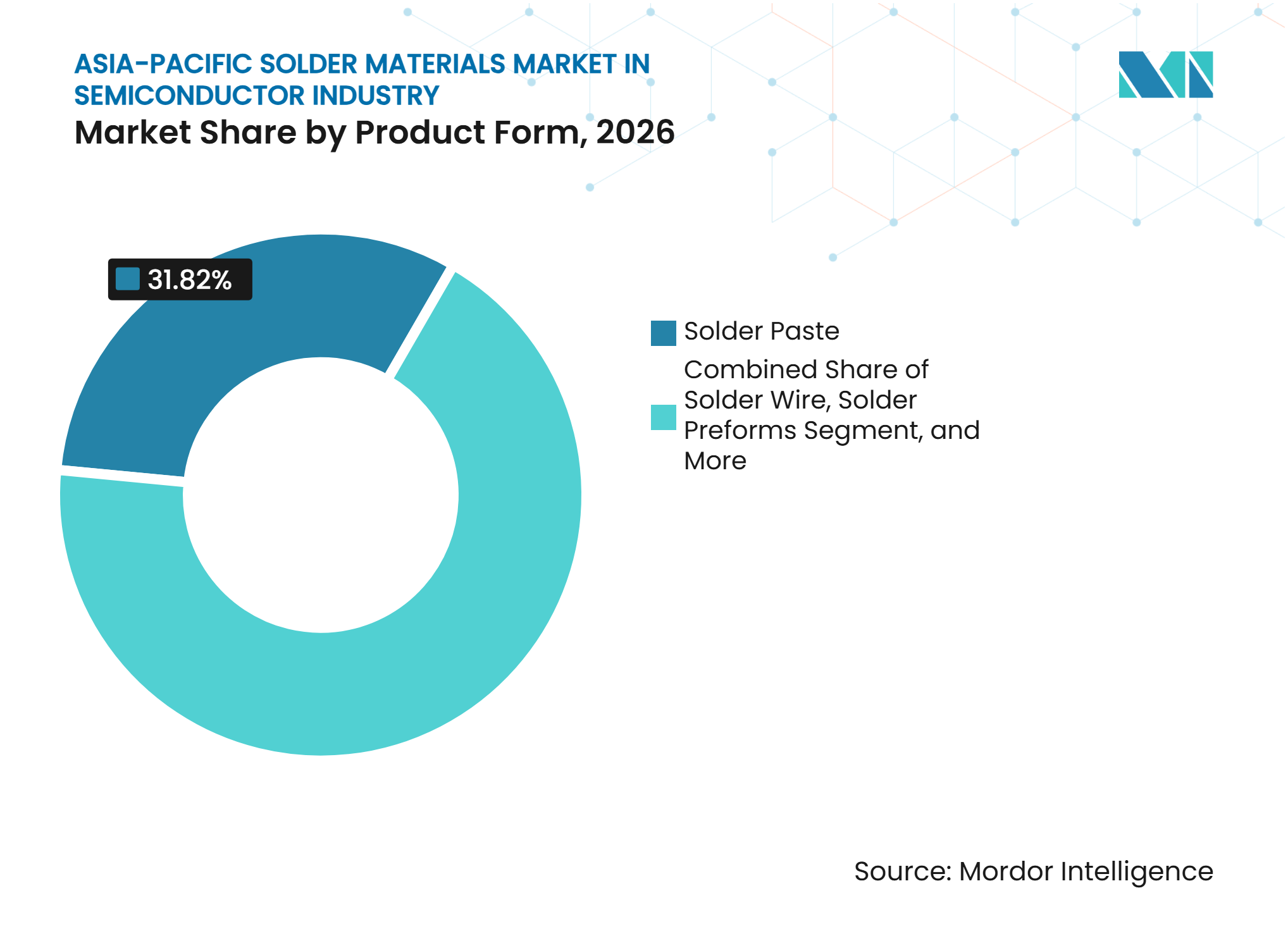
Solder Paste Leads, While Spheres Define the Growth AgendaSolder paste held 31.82% regional share in 2026 because it is used in stencil printing and jet dispensing for wafer-level chip-scale packaging, flip-chip, and system-in-package assembly. Its broad use makes it important across both high-volume and advanced package processes, including assemblies that need controlled deposit volumes at increasingly fine pitches. Shenmao Technology launched PF606-P279L in November 2025 for Type 6 and Type 7 powder applications and stencil apertures as small as 60 micrometers. MacDermid Alpha Electronics Solutions introduced ALPHA OM-377 in June 2026 for ultra-fine feature printing down to 008004 component sizes. These releases show how paste development is following tighter bump pitches and smaller package features, while also addressing transfer efficiency and common printing defects.
Solder balls and spheres are projected to expand at a CAGR of 10.82% from 2027 to 2032, making them the fastest-growing product form. HBM architectures require uniform microballs in the 25-80 micrometer range, and demand rises with higher stack counts and more complex die-to-die interconnect patterns. The technical requirement is not only volume but also dependable diameter control, consistent metallurgy, low oxide content, and low defect rates during ball attach. Solder preforms serve power electronics where large-area die attach needs flat and void-controlled layers that paste printing may not consistently deliver under demanding thermal conditions. The Asia-Pacific solder materials market in semiconductor industry also relies on solder wire, standalone powder, and flux for rework, through-hole, and substrate-level processes, although these categories have less pricing power than advanced bump-grade materials.


By Applicable Market:
Logic ICs Drive Volume, While Memory ICs Set the Growth PaceLogic ICs accounted for 32.63% regional share in 2026, reflecting their central role in processors, field-programmable gate arrays, and application-specific integrated circuits. Logic packages use formats such as CoWoS, fan-out, and flip-chip, which require dense and accurate bump arrays. Fine-pitch needs place greater emphasis on Type 6 and finer powder formulations, consistent flux behavior, and controlled paste deposition. Procurement can become concentrated around a limited number of advanced packaging programs, creating volume opportunities but also customer concentration risk. The Asia-Pacific solder materials industry depends on reliable technical support because a material failure can affect package yield, program timing, and customer confidence in the package process.
Memory ICs are projected to expand at a CAGR of 10.97% from 2027 to 2032 as HBM use increases in AI and high-performance computing platforms. Each HBM package requires many uniform solder microballs, so small deviations can affect attach yield at sub-100-micrometer pitches and increase rework risk. This gives approved suppliers a meaningful commercial advantage because changing materials can require extensive validation across the package, substrate, and customer reliability process. The Asia-Pacific solder materials market in semiconductor industry also serves compound semiconductors and power devices, a high-specification area because SiC and GaN applications need specialized die-attach materials. A 2025 review identifies silver and copper sintering as important approaches for demanding electronic interconnect applications. Analog ICs, sensors, MEMS, RF devices, and optical products provide steadier demand across automotive radar, communications, and data-center optical modules.
By Application and Process Step:
Wafer-Level Bump Formation Anchors Share and GrowthWafer-level bump formation accounted for 25.84% of the Asia-Pacific solder materials market size in 2026 and is projected to expand at a CAGR of 11.08% through 2032. This position reflects the movement of interconnect value toward wafer-level processes, where bump pitch directly affects electrical performance, thermal performance, and the eventual package footprint. Advanced wafer bumping uses copper pillar and solder-cap structures that require deposition at pitches below 55 micrometers, as well as careful control of deposit height and surface condition. The Asia-Pacific solder materials market in semiconductor industry therefore places high demands on Type 6 and Type 7 powder quality, sphere control, flux performance, and low-alpha characteristics. JEDEC and IPC reliability protocols raise the documentation and testing requirements for suppliers seeking approval in these processes.
Die-to-substrate interconnection through flip-chip remains the second-largest application step for high-I/O logic and memory packages. Controlled-collapse chip connection bumps at 100-130 micrometer pitch remain widely used in production because they support established high-volume assembly flows. Package-to-board interconnection through BGA and CSP ball attach provides stable demand across a broad set of devices and end-use applications. This step faces direct competition among established Chinese suppliers of solder materials, particularly where production volumes are large and specifications are less demanding. The Asia-Pacific solder materials market in semiconductor industry also includes backside die attach and package sealing for power and hermetic packages, but sintered silver and copper can replace solder in the highest-temperature configurations.

Geography Analysis
China
China held 32.38% regional share in 2026 because it combines wafer fabrication, outsourced assembly and test capacity, substrate production, and consumer electronics manufacturing. Local producers are expanding capabilities in bump-grade alloys and fine-pitch powder formulations to serve domestic logic and memory packaging lines. The regional supply chain benefits from close proximity between material suppliers, packaging houses, and electronics customers. China’s hazardous-substance standard GB 26572, scheduled to take effect in August 2027, will make compliance factors more important in product qualification.
India
India is projected to expand at a CAGR of 11.23% from 2027 to 2032 as government-backed ATMP and OSAT capacity shifts from policy commitments into material procurement. The government approved Semicon 2.0 in July 2026 with an outlay of INR 1,27,500 crore, or USD 15.2 billion, and included machines and materials as a supported pillar. This policy position makes packaging chemistries, including solder-related materials, more visible within the local semiconductor supply chain. The Asia-Pacific solder materials market in semiconductor industry can gain from qualification activity at new facilities because it shapes the approved supplier base over the forecast period. India’s growth is likely to favor suppliers that can pair product performance with local application support, timely samples, inventory availability, and compliance documentation.
Japan, South Korea, Taiwan, and the Rest of Asia-Pacific
Japan, South Korea, and Taiwan define much of the region’s technical standard for precision alloys, microballs, and wafer-bumping materials. Japanese suppliers, including Senju Metal Industry, Tamura Corporation, and Tanaka Precious Metal Technologies, are established in precision alloy and microball development. South Korean suppliers are positioned near HBM production lines, while Taiwan-based suppliers benefit from close access to advanced packaging customers and faster technical-service coordination. The Asia-Pacific solder materials market in semiconductor industry is also broadened by Southeast Asian packaging investment and the need for local engineering support. Indium Corporation highlighted AI material solutions at SEMICON Taiwan 2026, reflecting continuing focus on advanced packaging materials in the region.
Competitive Landscape
Market Concentration
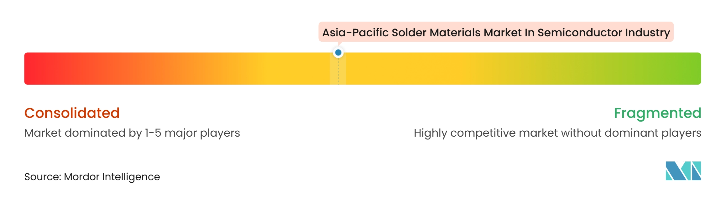
The Asia-Pacific solder materials market in semiconductor industry has moderate concentration in premium specialty alloys and greater fragmentation in commodity paste and wire. Senju Metal Industry, Tamura Corporation, Nihon Superior, and MacDermid Alpha Electronics Solutions are active in high-specification materials, including semiconductor-grade microballs and wafer-bumping pastes. Their positions are supported by alloy patents, controlled atomization capabilities, and established qualification records with packaging customers. In February 2025, MacDermid Alpha Electronics Solutions, Heraeus Electronics, and Henkel reported the final resolution of a patent dispute involving Senju’s M794 alloy and the Innolot technology. This outcome demonstrates the commercial importance of intellectual property in fatigue-resistant lead-free alloys.
Chinese suppliers compete strongly in mid-specification paste and solder powder by combining proximity to assembly customers with cost advantages. Their movement into leading-edge bump-grade spheres and automotive-qualified alloys depends on advances in metallurgy, process consistency, and long-cycle qualification. Opportunities remain in low-alpha solder balls for radiation-sensitive memory, copper-core spheres for BGA and CSP attach, BiSn low-temperature pastes that reduce warpage in fan-out panels, and sintered-compatible preforms for SiC power die attach. These applications address package-level requirements that standard commodity solder products do not meet.
MacDermid Alpha announced BondPad at electronica 2026, combining copper foil with Argomax sintered silver for topside SiC die attach. The company reported more than 75,000 power-cycling test cycles under a 110°C temperature swing, compared with 2,500 cycles for a conventional aluminum wirebond reference. Shenmao’s Type 6 and Type 7 paste release is another example of suppliers aligning products with fine-pitch production requirements. The Asia-Pacific solder materials market in semiconductor industry therefore rewards materials companies that combine technical differentiation with strong qualification support.
Leaders of Asia-Pacific Solder Materials Market In Semiconductor Industry
-
MacDermid Alpha Electronics Solutions
-
Senju Metal Industry Co., Ltd.
-
Tamura Corporation
-
Indium Corporation
-
Kester
- *Disclaimer: Major Players sorted in no particular order
Asia-Pacific Solder Materials Market In Semiconductor Industry Companies Covered in this Report
- MacDermid Alpha Electronics Solutions
- Senju Metal Industry Co., Ltd.
- Tamura Corporation
- Indium Corporation
- Kester
- Nihon Superior Co., Ltd.
- KOKI Company Ltd.
- Shenmao Technology, Inc.
- AIM Solder
- Henkel AG & Co. KGaA
- Heraeus Electronics
- Qualitek International, Inc.
- Harima Chemicals Group, Inc.
- Stannol GmbH & Co. KG
- DUKSAN Holdings Co., Ltd.
- Shenzhen Tongfang Electronic New-Material Co., Ltd.
- Shenzhen Vital New Material Co., Ltd.
- MK Electron Co., Ltd.
- Nihon Almit Co., Ltd.
- Tanaka Precious Metal Technologies Co., Ltd.
Recent Industry Developments in Asia-Pacific Solder Materials Market In Semiconductor Industry
- November 2026: MacDermid Alpha Electronics Solutions announced BondPad, a film-laminated copper-foil combining Argomax sintered silver for topside SiC die attach. Under a 110°C temperature swing, the technology achieved more than 75,000 power-cycling test cycles versus 2,500 cycles for a conventional aluminum wirebond reference, a change in reliability for automotive and industrial SiC power modules.
- July 2026: The Government of India approved Semicon 2.0 with an outlay of INR 1,27,500 crore, approximately USD 15.2 billion, explicitly adding machines and materials, including packaging chemistries, as a supported pillar. The program, announced by the Press Information Bureau, directs solder material procurement toward India-based or India-partnered suppliers for the first time.
- June 2026: MacDermid Alpha Electronics Solutions launched ALPHA OM-377, a no-clean solder paste for ultra-fine feature printing down to 008004 component sizes, delivering reduced head-in-pillow and non-wet open defect rates and consistent paste transfer efficiency across fine-pitch high-volume designs.
- November 2025: Shenmao Technology launched PF606-P279L, a no-clean ultra-fine pitch solder paste with Type 6 and Type 7 powder technology for mini-LED manufacturing, accommodating stencil apertures as small as 60 micrometers and available in SAC305 and multiple Sn-based alloys including Sn-Bi and Sn-Bi-Ag.
Scope of Report on Asia-Pacific Solder Materials Market In Semiconductor Industry
The Asia-Pacific Solder Materials Market in Semiconductor Industry Market encompasses the production and supply of specialized solder materials used in semiconductor assembly, packaging, and interconnection processes. These materials enable reliable electrical connections, thermal management, and mechanical bonding between semiconductor dies, substrates, and electronic components. The market covers solder-based solutions supporting advanced packaging technologies, high-density interconnections, and miniaturized semiconductor devices. Growing demand for high-performance chips, increasing semiconductor packaging complexity, and advancements in electronic manufacturing technologies drive the adoption of solder materials across the global semiconductor industry.
The Asia-Pacific Solder Materials Market in Semiconductor Industry Report is Segmented by Applicable Market (Logic ICs, Memory ICs, Compound Semiconductors and Power Devices, Analog ICs, Sensors, MEMS and RF Devices, and Optical and Photonic Devices), Product Form (Solder Paste, Solder Balls and Spheres, Solder Preforms, Solder Wire, Solder Fluxes, Standalone, and Solder Powder, Externally Sold), Application and Process Step(Wafer-Level Bump Formation, Die-to-Substrate Interconnection, Conventional Flip-Chip, Package-to-Board Interconnection, BGA and CSP Ball Attach, Backside Die Attach, and Package Sealing and Component Attachment), and Geography (China, Japan, South Korea, Taiwan, India, and Rest of Asia-Pacific). The Market Forecasts are Provided in Terms of Value (USD). The Market Forecasts are Provided in Terms of Value (USD).
Segmentation Overview
| Logic ICs |
| Memory ICs |
| Compound Semiconductors and Power Devices |
| Analog ICs |
| Sensors, MEMS and RF Devices |
| Optical and Photonic Devices |
| Solder Paste |
| Solder Balls and Spheres |
| Solder Preforms |
| Solder Wire |
| Solder Fluxes, Standalone |
| Solder Powder, Externally Sold |
| Wafer-Level Bump Formation |
| Die-to-Substrate Interconnection, Conventional Flip-Chip |
| Package-to-Board Interconnection, BGA and CSP Ball Attach |
| Backside Die Attach |
| Package Sealing and Component Attachment |
| China |
| Japan |
| South Korea |
| Taiwan |
| India |
| Rest of Asia-Pacific |
| By Applicable Market | Logic ICs |
| Memory ICs | |
| Compound Semiconductors and Power Devices | |
| Analog ICs | |
| Sensors, MEMS and RF Devices | |
| Optical and Photonic Devices | |
| By Product Form | Solder Paste |
| Solder Balls and Spheres | |
| Solder Preforms | |
| Solder Wire | |
| Solder Fluxes, Standalone | |
| Solder Powder, Externally Sold | |
| By Application and Process Step | Wafer-Level Bump Formation |
| Die-to-Substrate Interconnection, Conventional Flip-Chip | |
| Package-to-Board Interconnection, BGA and CSP Ball Attach | |
| Backside Die Attach | |
| Package Sealing and Component Attachment | |
| By Geography | China |
| Japan | |
| South Korea | |
| Taiwan | |
| India | |
| Rest of Asia-Pacific |
Key Questions Answered in the Report
What is the Asia-Pacific solder materials market in semiconductor industry size?
The market is valued at USD 210.01 million in 2026 and is projected to reach USD 385.88 million by 2032, registering a CAGR of 10.69% from 2027 to 2032. Demand is tied to finer interconnect requirements in advanced packaging.
What is driving demand for semiconductor solder materials in Asia-Pacific?
Advanced packaging for AI, HBM, and chiplets raises demand for fine-pitch solder balls, high-quality paste, and tightly controlled interconnect materials. New packaging capacity also widens the regional qualification pipeline for approved suppliers.
Which product form leads semiconductor solder materials demand in Asia-Pacific?
Solder paste leads with a 31.82% share in 2026 because it supports stencil printing and jet dispensing across several package types. Solder balls and spheres have the highest projected CAGR of 10.82% through 2032.
Why are memory ICs important for solder materials suppliers?
Memory ICs are projected to expand at a CAGR of 10.97% through 2032 as HBM packages use large volumes of tightly specified solder microballs. Yield performance and diameter consistency are important during qualification.
Which application has the strongest outlook for solder materials?
Wafer-level bump formation held 25.84% share in 2026 and is projected to expand at a CAGR of 11.08% through 2032. The process needs precise deposition, controlled bump geometry, and stringent reliability documentation.
Which Asia-Pacific countries offer the strongest semiconductor packaging opportunity?
China remains the largest country market with 32.38% share in 2026, while India has the highest projected CAGR of 11.23% through 2032. Indias policy support includes packaging machines and materials.