Advanced Packaging Inspection Systems Market Size and Share
Market Overview
| Study Period | 2020 - 2031 |
|---|---|
| Market Size (2026) | USD 3.67 Billion |
| Market Size (2031) | USD 6.22 Billion |
| Growth Rate (2026 - 2031) | 11.13 % |
| Fastest Growing Market | North America |
| Largest Market | Asia-Pacific |
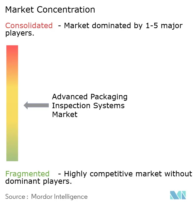
| Market Concentration | Medium |
Major Players *Disclaimer: Major Players sorted in no particular order Image © Mordor Intelligence. Reuse requires attribution under CC BY 4.0. | |
Advanced Packaging Inspection Systems Market Analysis by Mordor Intelligence
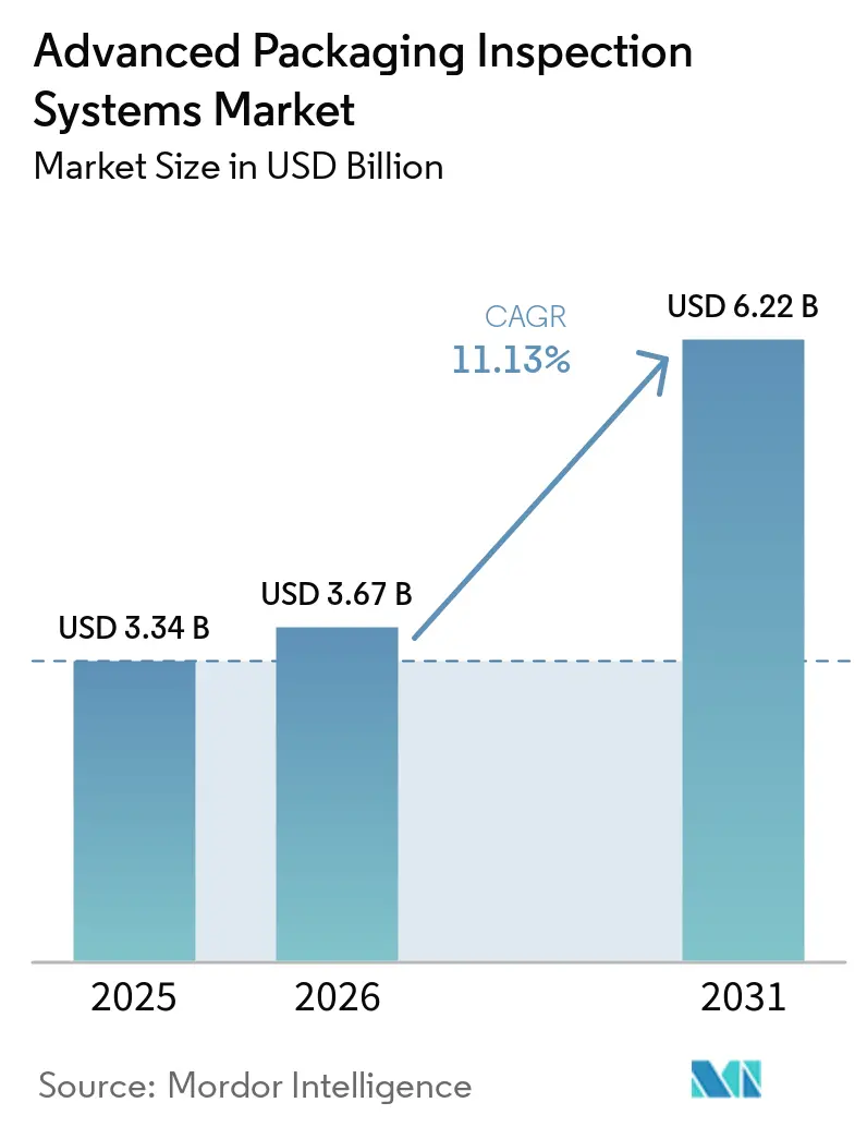
The advanced packaging inspection systems market size was USD 3.34 billion in 2025, and USD 3.67 billion in 2026, and is projected to reach USD 6.22 billion by 2031, growing at a CAGR of 11.13% during 2026-2031. Growth in the advanced packaging inspection systems market reflects the semiconductor sector's shift toward heterogeneous integration as conventional node scaling becomes less economical at the leading edge. More complex packages combine dies made on different process nodes, so manufacturers need tighter control of defects throughout assembly. AI accelerator output increasingly depends on advanced packaging capacity, rather than wafer fabrication capacity alone. Higher die values also make broad inline inspection coverage more attractive, because a defect can affect a completed multi-die device. Inspection is moving beyond pass-fail screening toward process control that supports yield improvement.
Key Report Takeaways
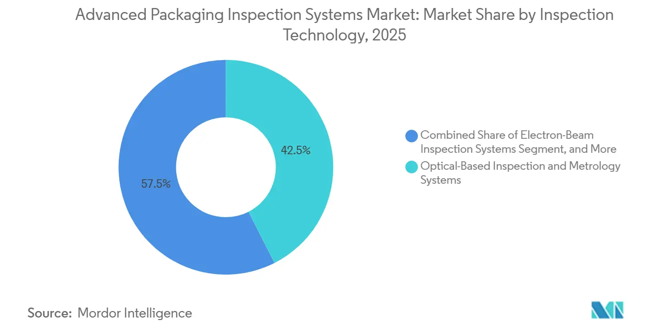
- By inspection technology, optical-based inspection and metrology systems held 42.51% of the advanced packaging inspection systems market share in 2025, while X-ray and computed tomography inspection systems are projected to expand at a 14.80% CAGR through 2031.
- By inspection stage, post-assembly inspection held 34.26% share in 2025, while wafer-level inspection is projected to expand at a 14.29% CAGR through 2031.
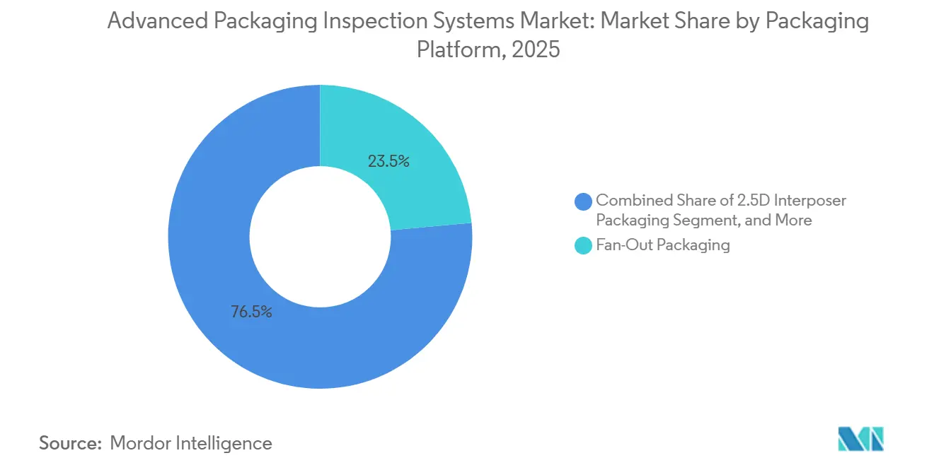
- By packaging platform, fan-out packaging held a 23.54% share of the advanced packaging inspection systems market in 2025, while hybrid-bonded packaging is projected to expand at a 15.94% CAGR through 2031.
- By end-user industry, data centers and high-performance computing held 33.92% share in 2025 and are projected to expand at a 15.66% CAGR through 2031.
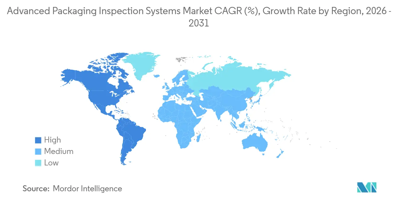
- By geography, Asia-Pacific held 59.81% share in 2025, while North America in the advanced packaging inspection systems market is projected to expand at a 14.50% CAGR through 2031.
Note: Market size and forecast figures in this report are generated using Mordor Intelligence’s proprietary estimation framework, updated with the latest available data and insights as of January 2026.
Market Trends and Insights
Drivers Impact Analysis of Advanced Packaging Inspection Systems Market*
| DRIVER | (~) % IMPACT ON CAGR FORECAST | GEOGRAPHIC RELEVANCE | IMPACT TIMELINE |
|---|---|---|---|
| AI and High-Performance Computing Driving Heterogeneous Integration | +3.2% | Global, concentrated in Asia-Pacific and North America | Short term (≤ 2 years) |
| Rising Hybrid Bonding and Fine-Pitch Interconnect Adoption | +2.4% | Global, led by Taiwan, South Korea, Japan, the United States, and Europe | Medium term (2-4 years) |
| Expansion of HBM and 3D Memory Stacking | +1.8% | Asia-Pacific, with spillover to North America | Short term (≤ 2 years) |
| Government Incentives for Domestic Advanced Packaging Capacity | +1.5% | North America and Europe, extending to India and Southeast Asia | Medium term (2-4 years) |
| Growth of Panel-Level Packaging and Glass-Core Substrates | +0.9% | Asia-Pacific and North America, with emerging European activity | Long term (≥ 4 years) |
| Increasing Yield Economics of Inline Multimodal Inspection | +0.6% | Global, especially high-volume CoWoS and HBM hubs | Medium term (2-4 years) |
| Source: Mordor Intelligence | |||
AI and High-Performance Computing Driving Heterogeneous Integration
AI accelerator packages are among the most difficult devices to inspect because they combine several dies, dense interconnect structures, and materials with different process histories. Every packaging wafer requires checks of incoming substrate quality, copper redistribution layer patterning, micro-bump coplanarity, die placement, and final package integrity before it can support a high-value system. KLA stated that advanced packaging revenue in its semiconductor process control portfolio was expected to rise from USD 635 million in 2025 to USD 1 billion in 2026.[1]KLA Corporation, “KLA Corporation Reports Fiscal 2026 Third Quarter Results,” KLA Corporation, roic.ai This company result links process-control spending to added packaging capacity and to the larger number of measurement steps used on heterogeneous packages. The advanced packaging inspection systems market benefits when capacity additions require inspection at multiple manufacturing stages rather than relying on a final check alone. Tool demand in the advanced packaging inspection systems market also becomes less dependent on chip volumes because costly multi-die packages require greater inspection coverage for each finished unit.
Rising Hybrid Bonding and Fine-Pitch Interconnect Adoption
Hybrid bonding requires inspection methods that can address very small features, buried interfaces, surface conditions, and production throughput at the same time. An ASM Electronic Device Failure Analysis Society study found that no single method provides nanoscale resolution, full-field coverage, subsurface visibility, and manufacturing-compatible throughput across all hybrid-bonding stages. Manufacturers in the advanced packaging inspection systems market, therefore, use optical, infrared, acoustic, and X-ray approaches at distinct points in the bonding flow, rather than treating hybrid-bond inspection as one tool purchase. Onto Innovation described in-line hybrid-bonding tools that combine 3D metrology for particle-height measurement with infrared inspection that can identify voids in dielectric layers.[2]Onto Innovation Inc., “Enabling In-Line Process Control for Hybrid Bonding Applications,” Onto Innovation, ontoinnovation.com Nova announced in July 2026 that a leading global foundry had selected its WMC platform as its tool of record for advanced packaging measurements following a competitive evaluation. This shift expands the advanced packaging inspection systems market because hybrid bonding transforms a single inspection point into a broader process-control sequence with multiple physical measurement requirements.
Expansion of HBM and 3D Memory Stacking
HBM4 and taller memory stacks introduce alignment, warpage, bonding, and continuity concerns throughout the packaging flow, and these concerns must be managed at successive bonding steps. SK Hynix stated that its 12-layer HBM4 entered mass production in 2026 and its 16-layer product was in qualification. Samsung redesigned an HBM dummy die with a stepped structure to address delamination, micro-cracking, and warpage in 16-layer configurations. Cohu raised its 2025 HBM revenue estimate to USD 10 million to USD 11 million after further Neon orders and reported its first system configured for HBM4 inspection. As stacks become taller, individual dies become thinner and more prone to warpage, increasing requirements across the advanced packaging inspection systems market for higher-resolution inspection and planarity metrology. The advanced packaging inspection systems market gains demand at both bonding and final inspection stages as manufacturers seek to limit the risk of defects in stacked devices.
Government Incentives for Domestic Advanced Packaging Capacity
Public funding is broadening the advanced packaging inspection systems market across the locations where advanced packaging capacity can be built and where inspection equipment suppliers need local support capabilities. The U.S. Department of Commerce finalized USD 1.4 billion in National Advanced Packaging Manufacturing Program awards in January 2025. The awards included USD 100 million each for Absolics, Applied Materials, and Arizona State University activities involving glass-core packaging, silicon-core substrates, and fan-out wafer-level processing. In July 2026, the department announced letters of intent totaling USD 874 million for research and development in advanced packaging, substrates, materials, integrated photonics, and memory. New facilities create equipment demand along with the need for field service and applications support in regions with smaller installed process-control bases. The advanced packaging inspection systems market can gain from this new capacity even where the surrounding packaging ecosystem is still developing.
Restraints Impact Analysis of Advanced Packaging Inspection Systems Market*
| RESTRAINT | (~) % IMPACT ON CAGR FORECAST | GEOGRAPHIC RELEVANCE | IMPACT TIMELINE |
|---|---|---|---|
| High Capital and Total Cost of Ownership | -2.2% | Global, most acute for emerging OSATs in Southeast Asia and South America | Short term (≤ 2 years) |
| Shortage of Advanced Packaging Metrology Talent | -1.4% | Global, particularly Taiwan, South Korea, and new U.S. fabrication clusters | Medium term (2-4 years) |
| Specialty Component and Supply-Chain Constraints | -0.9% | Global, concentrated in precision optics, laser sources, and high-purity detectors | Short term (≤ 2 years) |
| Data-Integration and Cybersecurity Risk in Connected Inspection | -0.5% | Global, with greater sensitivity in the United States, Europe, and Japan | Medium term (2-4 years) |
| Source: Mordor Intelligence | |||
High Capital and Total Cost of Ownership
Advanced packaging inspection systems require significant capital outlay when a production line uses several inspection technologies, and the equipment must also be integrated with cleanroom operations and maintenance practices. A hybrid-bonding line may need optical, infrared, acoustic, and X-ray tools, with each system serving a different physical measurement requirement. That cost burden is especially difficult for outsourced semiconductor assembly and test providers with narrower equipment budgets and less room to fund full inline coverage. Onto Innovation launched Dragonfly G5 in March 2026 with an optics and illumination design intended to support several HBM4-related applications on one platform. The platform's design reflects customer demand for broader capability without adding a separate tool for every application, while preserving the sensitivity needed for advanced package workflows. Smaller participants in the advanced packaging inspection systems market may continue to use sampling where comprehensive inline inspection is difficult to fund, even though sampling can leave more yield risk in complex multi-die products.
Shortage of Advanced Packaging Metrology Talent
The specialized workforce needed to operate, maintain, and qualify inspection tools remains limited as new packaging facilities expand. Taiwan's semiconductor sector reported a shortage of 34,000 workers in May 2025, while openings in operations, technical support, and maintenance had risen 67% from October 2023. The shortage affects process-control roles because the work requires equipment knowledge, package-structure understanding, and the ability to interpret yield data through each manufacturing step. Longer qualification cycles at customer sites can delay equipment acceptance, increase the field-application burden on vendors, and slow the time between shipment and full production use. New North American clusters face a related challenge because facility construction and equipment installation can advance faster than local workforce development. This constraint may limit how quickly the advanced packaging inspection systems market converts announced capacity into productive tool installations and recurring service activity.
*Our forecasts treat driver/restraint impacts as directional, not additive. The impact forecasts reflect baseline growth, mix effects, and variable interactions.
Advanced Packaging Inspection Systems Market Segment Analysis
By Inspection Technology:
Optical Systems Retain Scale While X-Ray Gains GroundOptical-based inspection and metrology systems held 42.51% of the advanced packaging inspection systems market share in 2025. Their leading position reflects high throughput, broad use across wafer-level and post-assembly flows, and an established installed base at wafer fabs and outsourced assembly sites. These systems support redistribution layer critical-dimension measurement, bump coplanarity checks, die-shift detection, and macro-defect screening across several package types. Their use in fan-out and flip-chip production aligns with the need to manage inspection speed and cost in high-volume flows. Onto Innovation launched Dragonfly G5 in March 2026 with stated 150 nm defect sensitivity and multi-mode illumination for advanced packaging applications.
Infrared and thermal systems find subsurface voids and delamination in stacked-die structures, while acoustic systems identify underfill and encapsulant issues beyond the reach of surface optical methods. Electron-beam inspection provides electrical-contrast imaging for through-silicon vias and back-end interconnects, and an SPIE paper reported defective-die capture rates up to 4.3 times higher through AI-guided computational sampling.[3]SPIE, “Computational Guided Dynamic Sampling E-Beam Inspection in High-Volume Manufacturing Automation With ASML's Virtual Computing Platform,” SPIE Advanced Lithography and Patterning, spiedigitallibrary.org X-ray and computed tomography inspection systems are projected to grow at a 14.80% CAGR through 2031, the highest rate in this segmentation. Research in Microelectronics Reliability showed that high-resolution nano-CT detected sub-micron voids and cracks in 20 µm micro-bumps during a 30-second overview scan. This capability supports inspection of buried joints, HBM continuity, and hybrid-bond interfaces that optical systems cannot directly assess.



By Inspection Stage:
Post-Assembly Holds the Installed Base While Wafer-Level Inspection AcceleratesPost-assembly inspection held 34.26% of the share in the advanced packaging inspection systems sector in 2025. Its position reflects the installed base of automated optical inspection and 3D inspection systems used after dicing and during package assembly. These tools assess package appearance, solder-related features, alignment, and other visible conditions before shipment. The category remains necessary for every package, including devices made through mature packaging methods. It also serves outsourced assembly operations that process high volumes across multiple customer programs.
Wafer-level inspection in the advanced packaging inspection systems market is projected to expand at a 14.29% CAGR through 2031 because defects found before die attach can prevent loss in a completed multi-die package. A December 2025 review in the Journal of Manufacturing Science and Engineering found that through-silicon vias, hybrid bonding interfaces, and micro-bump arrays are raising requirements for surface and subsurface inspection.[4]ASME, “A Review of Through-Silicon Via Inspection and Metrology Technology for Advanced Semiconductor Packaging,” Journal of Manufacturing Science and Engineering, asmedigitalcollection.asme.org Nova released the WMC in August 2025 as a modular optical metrology platform for 2.5D and 3D integration, hybrid bonding, and different wafer sizes. Die-level inspection prevents known-defective dies from entering multi-die assemblies, while final inspection and failure analysis feed findings back to upstream process teams. Cohu stated that its Neon platform was being qualified at a Taiwan-based outsourced assembly site for HBM3, HBM4, and HBM4E applications in 2026.
By Packaging Platform:
Fan-Out Holds the Largest Share While Hybrid Bonding Expands FastestFan-out packaging held 23.54% of the share in the advanced packaging inspection systems sector in 2025. Its scale in the advanced packaging inspection systems market is tied to wafer-level manufacturing compatibility and use in mobile processors, RF front ends, and networking chips. Inspection supports redistribution layer checks, die placement verification, and defect screening across high-volume production. The platform has mature manufacturing methods, but tighter-pitch requirements support upgrades to higher-resolution optical tools. Fan-in packaging also benefits from this renewal cycle as its redistribution layers become more demanding.
Hybrid-bonded packaging is projected to grow at a 15.94% CAGR through 2031. Direct copper-to-copper bonding at sub-micron pitch enables higher interconnect density than bump-based alternatives. The process requires tight control of surface planarity across 300 mm wafers because slight nanotopography changes can affect bond quality. Nova described vertical traveling scatterometry with machine learning for monitoring copper recess during hybrid-bonding chemical mechanical polishing with sub-nanometer fidelity. 2.5D interposer systems require checks of micro-bump coplanarity, redistribution layer integrity, and interposer quality, while 3D integrated circuit and HBM packaging needs known-good-die verification, stack alignment, and through-silicon-via continuity checks. Panel-level, system-in-package, embedded-die, and chiplet configurations add varied materials and defect modes that require tailored inspection strategies.
By End-User Industries:
Data Centers and High-Performance Computing Lead on Both Scale and GrowthData centers and high-performance computing held 33.92% share of the advanced packaging inspection systems market in 2025. The segment is projected to grow at a 15.66% CAGR through 2031, the highest rate among end-user industries. AI processors use HBM, 2.5D interposers, and other dense package architectures that require several inspection and metrology steps. Camtek reported that advanced packaging represented 75% of revenue and 80% of year-to-date orders in the second quarter of 2026. The company identified HBM, CoWoS, and similar AI data-center applications as its major demand sources.
Consumer electronics remain an established base in the advanced packaging inspection systems market for fan-out and flip-chip packaging inspection, but longer device replacement cycles and more stable package complexity temper its growth. Automotive and electric vehicle packages require strict reliability practices for powertrain and advanced driver-assistance systems. Telecommunications and networking packages must support high-frequency performance and controlled impedance. Healthcare and medical devices require rigorous inspection records because implantable and diagnostic packages undergo extensive reliability testing. Aerospace and defense applications have lower volumes but can support long-duration supply arrangements, while research institutions test terahertz, GaN-based electron-beam, and correlative nano-CT approaches before wider production use.
Geography Analysis
APAC Advanced Packaging Inspection Systems Market
Asia-Pacific held 59.81% of the share in the advanced packaging inspection systems sector in 2025. Its position follows the region's concentration of advanced packaging capacity, memory production, and outsourced semiconductor assembly operations. Taiwan accounted for nearly 50% of global IC packaging and testing output in 2024, based on ITRI data reported by the Taipei Times, and South Korea adds major HBM packaging activity. Japan contributes precision optics, electron-beam suppliers, outsourced assembly operations, and memory packaging capacity. These production centers make the region important for new equipment installations and field service.
China and ASEAN Advanced Packaging Inspection Systems Market
China has a large legacy packaging base within the advanced packaging inspection systems market and an increasing interest in domestically sourced inspection equipment. Camtek reported that China represented 45% of its 2026 revenue. Malaysia, Vietnam, and Singapore are gaining relevance as outsourced assembly capacity expands beyond Taiwan. Their capacity can absorb part of the demand when lead times at established facilities lengthen.
The Americas and EMEA Advanced Packaging Inspection Systems Market
North America in the advanced packaging inspection systems market is projected to grow at a 14.50% CAGR through 2031, making it the fastest-growing geography. SK Hynix held a groundbreaking ceremony in August 2026 for an HBM packaging facility in Indiana that was expected to be a North American HBM production base by 2030. U.S. public awards support packaging research, pilot capacity, substrate development, and materials work.[5]National Institute of Standards and Technology, “Department of Commerce Announces Letters of Intent With 7 Companies for USD 874 Million to Accelerate Semiconductor RandD,” National Institute of Standards and Technology, nist.gov Canada supports packaging research, and Mexico has a role in back-end assembly and test. Europe has a more modest position, led by German and Dutch suppliers serving X-ray, X-ray fluorescence, and atomic-force-metrology applications. South America and the Middle East and Africa remain smaller markets where demand follows contract assembly and test investment.

Competitive Landscape
The advanced packaging inspection systems market has a concentrated leading tier and a diverse group of specialized suppliers. KLA has the broadest process-control portfolio among the named companies. It reported total fiscal 2026 revenue of USD 13.579 billion, including USD 12.245 billion from its semiconductor process control segment. This scale supports applications engineering and field service across major packaging locations. Camtek and Onto Innovation actively compete in the advanced packaging inspection systems market for packaging-specific optical inspection and metrology.
Camtek received combined orders above USD 105 million in June 2026 from a tier-1 outsourced assembly and test provider and a leading HBM manufacturer. Onto Innovation launched Dragonfly G5 in March 2026, with stated 150 nm defect sensitivity and fivefold throughput improvement over prior tools. In April 2026, Onto Innovation announced the qualification of Dragonfly G5 for 2.5D AI packaging applications. Nova has focused on modular metrology for hybrid bonding, and its selection of WMC as the tool of record provides a reference point for high-volume packaging. Cohu is extending Neon across HBM inspection and AI data-center processor applications.
Applied Materials agreed in May 2026 to acquire the NEXX business from ASMPT, adding large-area packaging deposition capability alongside its existing inspection and metrology assets. NVIDIA and TSMC announced a collaboration in June 2026 that leverages NVIDIA Metropolis and the TAO Toolkit for AI-powered defect inspection in TSMC's manufacturing. TASMIT launched a glass-substrate inspection system in February 2025 for double-sided and internal-defect inspection. Specialists retain opportunities where throughput, sensitivity, and material-specific capabilities differ from those of leading optical platforms.
Advanced Packaging Inspection Systems Industry Leaders
KLA Corporation
Onto Innovation Inc.
Camtek Ltd.
Cohu, Inc.
Intekplus Co., Ltd.
- *Disclaimer: Major Players sorted in no particular order
Advanced Packaging Inspection Systems Market Companies Covered in this Report
- KLA Corporation
- Onto Innovation Inc.
- Camtek Ltd.
- Cohu, Inc.
- Intekplus Co., Ltd.
- Semiconductor Technologies and Instruments Pte. Ltd.
- Lasertec Corporation
- Unity Semiconductor SAS
- Shenzhen Skyverse Technology Co., Ltd.
- Cheng Mei Instrument Technology Co., Ltd.
- Chroma ATE Inc.
- Toray Engineering Co., Ltd.
- TASMIT, Inc.
- Confovis GmbH
- Nova Ltd.
- Bruker Corporation
- Nearfield Instruments B.V.
- Comet Yxlon GmbH
- Hitachi High-Tech Corporation
- Tokyo Electron Limited
- JEOL Ltd.

Recent Industry Developments in Advanced Packaging Inspection Systems Market
- August 2026: SK Hynix held the groundbreaking ceremony for its USD 4 billion HBM advanced packaging facility in West Lafayette, Indiana. The factory, supported by USD 458 million in CHIPS Act direct funding and USD 712 million in state incentives, is scheduled to open its first cleanroom for packaging operations in October 2028 and is positioned as a key HBM production base in North America by 2030.
- July 2026: Nova Ltd. announced that its Nova WMC platform was selected as the tool-of-record by a leading global foundry for multiple-layer measurement in the most advanced packaging processes, following a competitive evaluation against major incumbents. This designation signals the WMC's emergence as a reference tool for advanced packaging metrology in high-volume manufacturing.
- July 2026: The U.S. Department of Commerce announced letters of intent totaling USD 874 million with 7 companies for RandD covering advanced packaging, substrates, materials, integrated photonics, and memory for next-generation AI systems. Recipients include Multibeam Corporation, with up to USD 140 million for advanced packaging multi-chip stacking technology, and Thintronics, with up to USD 50 million for inter-layer dielectrics.
- June 2026: Camtek received combined orders exceeding USD 105 million, USD 55 million from a tier-1 OSAT for AI packaging applications and over USD 50 million in Hawk systems from a leading HBM manufacturer, all for 2027 delivery. This order block extended Camtek's backlog visibility and reflected accelerating HBM4 manufacturing ramp timelines.


Global Advanced Packaging Inspection Systems Market Report Scope
The advanced packaging inspection systems market comprises automated optical, X-ray, and multi-modal inspection equipment used to detect defects, measure critical dimensions, and ensure quality control in advanced semiconductor packaging processes such as 2.5D/3D integration, fan-out wafer-level packaging (FOWLP), system-in-package (SiP), and chiplet-based architectures. These systems employ high-resolution imaging, machine vision, AI-powered defect classification, and precision metrology to identify voids, misalignments, solder joint defects, warpage, and interconnect anomalies throughout packaging assembly, enabling manufacturers to maintain yield rates, reduce rework, and meet stringent reliability requirements as packaging densities increase and feature sizes shrink to support high-performance computing, AI accelerators, and mobile applications.
The Advanced Packaging Inspection Systems Market Report is Segmented by Inspection Technology (Optical-Based Inspection and Metrology Systems, Infrared and Thermal Inspection Systems, X-Ray and Computed Tomography Inspection Systems, Electron-Beam Inspection Systems, and Acoustic and Other Inspection Systems), Inspection Stage (Wafer-Level Inspection, Die-Level and Component Inspection, Post-Assembly Inspection, and Final Inspection and Failure Analysis), Packaging Platform (2.5D Interposer Packaging, 3D Integrated Circuit and HBM Packaging, Fan-Out Packaging, Fan-In Packaging, Panel-Level Packaging, System-in-Package, Hybrid-Bonded Packaging, and Embedded-Die and Chiplet Packaging), End-User Industries (Consumer Electronics, Data Centers and High-Performance Computing, Automotive and Electric Vehicles, Telecommunications and Networking, Healthcare and Medical Devices, Aerospace and Defense, Research and Academic Institutions, and Other End-User Industries), and Geography (North America, South America, Europe, Asia-Pacific, and Middle East and Africa). The Market Forecasts are Provided in Terms of Value (USD).
| Optical-Based Inspection and Metrology Systems |
| Infrared and Thermal Inspection Systems |
| X-Ray and Computed Tomography Inspection Systems |
| Electron-Beam Inspection Systems |
| Acoustic and Other Inspection Systems |
| Wafer-Level Inspection |
| Die-Level and Component Inspection |
| Post-Assembly Inspection |
| Final Inspection and Failure Analysis |
| 2.5D Interposer Packaging |
| 3D Integrated Circuit and HBM Packaging |
| Fan-Out Packaging |
| Fan-In Packaging |
| Panel-Level Packaging |
| System-in-Package |
| Hybrid-Bonded Packaging |
| Embedded-Die and Chiplet Packaging |
| Consumer Electronics |
| Data Centers and High-Performance Computing |
| Automotive and Electric Vehicles |
| Telecommunications and Networking |
| Healthcare and Medical Devices |
| Aerospace and Defense |
| Research and Academic Institutions |
| Other End-User Industries |
| North America | United States | |
| Canada | ||
| Mexico | ||
| South America | Brazil | |
| Argentina | ||
| Rest of South America | ||
| Europe | Germany | |
| United Kingdom | ||
| France | ||
| Italy | ||
| Spain | ||
| Rest of Europe | ||
| Asia-Pacific | China | |
| Japan | ||
| India | ||
| South Korea | ||
| ASEAN | ||
| Rest of Asia-Pacific | ||
| Middle East and Africa | Middle East | Saudi Arabia |
| United Arab Emirates | ||
| Turkey | ||
| Rest of the Middle East | ||
| Africa | South Africa | |
| Nigeria | ||
| Rest of Africa | ||
| By Inspection Technology | Optical-Based Inspection and Metrology Systems | ||
| Infrared and Thermal Inspection Systems | |||
| X-Ray and Computed Tomography Inspection Systems | |||
| Electron-Beam Inspection Systems | |||
| Acoustic and Other Inspection Systems | |||
| By Inspection Stage | Wafer-Level Inspection | ||
| Die-Level and Component Inspection | |||
| Post-Assembly Inspection | |||
| Final Inspection and Failure Analysis | |||
| By Packaging Platform | 2.5D Interposer Packaging | ||
| 3D Integrated Circuit and HBM Packaging | |||
| Fan-Out Packaging | |||
| Fan-In Packaging | |||
| Panel-Level Packaging | |||
| System-in-Package | |||
| Hybrid-Bonded Packaging | |||
| Embedded-Die and Chiplet Packaging | |||
| By End-User Industries | Consumer Electronics | ||
| Data Centers and High-Performance Computing | |||
| Automotive and Electric Vehicles | |||
| Telecommunications and Networking | |||
| Healthcare and Medical Devices | |||
| Aerospace and Defense | |||
| Research and Academic Institutions | |||
| Other End-User Industries | |||
| By Geography | North America | United States | |
| Canada | |||
| Mexico | |||
| South America | Brazil | ||
| Argentina | |||
| Rest of South America | |||
| Europe | Germany | ||
| United Kingdom | |||
| France | |||
| Italy | |||
| Spain | |||
| Rest of Europe | |||
| Asia-Pacific | China | ||
| Japan | |||
| India | |||
| South Korea | |||
| ASEAN | |||
| Rest of Asia-Pacific | |||
| Middle East and Africa | Middle East | Saudi Arabia | |
| United Arab Emirates | |||
| Turkey | |||
| Rest of the Middle East | |||
| Africa | South Africa | ||
| Nigeria | |||
| Rest of Africa | |||


Key Questions Answered in the Report
What is the size of the advanced packaging inspection systems market?
The advanced packaging inspection systems market size was USD 3.34 billion in 2025, and USD 3.67 billion in 2026, and is projected to reach USD 6.22 billion by 2031, growing at a CAGR of 11.13% during 2026-2031.
What is driving demand for advanced packaging inspection systems?
Heterogeneous integration, AI accelerators, hybrid bonding, and HBM stacking are increasing inspection needs across packaging workflows.
Which inspection technology leads advanced packaging inspection systems?
Optical-based inspection and metrology systems led with 42.51% share in 2025, supported by high throughput and broad process coverage.
Which packaging platform is growing fastest?
Hybrid-bonded packaging is projected to grow at a 15.94% CAGR through 2031 because it requires stringent control of fine-pitch copper bonding.
Which end-user application has the strongest growth?
Data centers and high-performance computing held 33.92% share in 2025 and are projected to grow at a 15.66% CAGR through 2031.
Which region is expanding fastest?
North America in the advanced packaging inspection systems market is projected to grow at a 14.50% CAGR through 2031 as public programs and new packaging facilities support domestic capacity.
Page last updated on: