White-Light Interferometry Systems Market Size and Share
Market Overview
| Study Period | 2020 - 2031 |
|---|---|
| Market Size (2026) | USD 310.52 Million |
| Market Size (2031) | USD 457.68 Million |
| Growth Rate (2026 - 2031) | 8.07 % |
| Fastest Growing Market | Asia-Pacific |
| Largest Market | Asia-Pacific |
| Market Concentration | Medium |
Major Players *Disclaimer: Major Players sorted in no particular order Image © Mordor Intelligence. Reuse requires attribution under CC BY 4.0. | |
White-Light Interferometry Systems Market Analysis by Mordor Intelligence
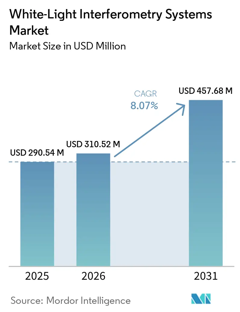
The white-light interferometry systems market size was valued at USD 290.54 million in 2025 and is estimated to expand from USD 310.52 million in 2026 to reach USD 457.68 million by 2031, at a CAGR of 8.07% during the forecast period (2026-2031). Demand is increasingly tied to more complex semiconductor production steps, rather than only to higher wafer volumes. Gate-all-around transistor designs create vertical structures that require repeatable, non-contact surface measurement during process qualification. Advanced packaging also increases the number of bonding surfaces that need topography verification. Vendors are responding with inline systems, software analytics, and hybrid measurement platforms. Semiconductor investment cycles remain important, although broader use across packaging, precision manufacturing, optics, and medical production provides some support during slower capital spending periods.
Key Report Takeaways
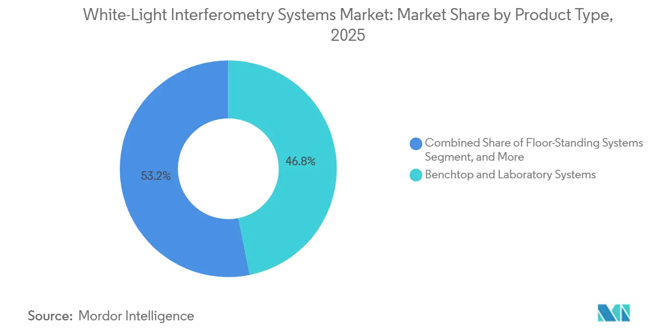
- By product type, Benchtop and Laboratory Systems held 46.83% of the white-light interferometry systems market share in 2025, while Inline and On-Machine Systems are projected to expand at an 8.46% CAGR through 2031.
- By technology, Coherence Scanning Interferometry held 44.67% revenue share in 2025, while AI-Enabled Interferometric Analysis is projected to expand at an 8.37% CAGR through 2031.
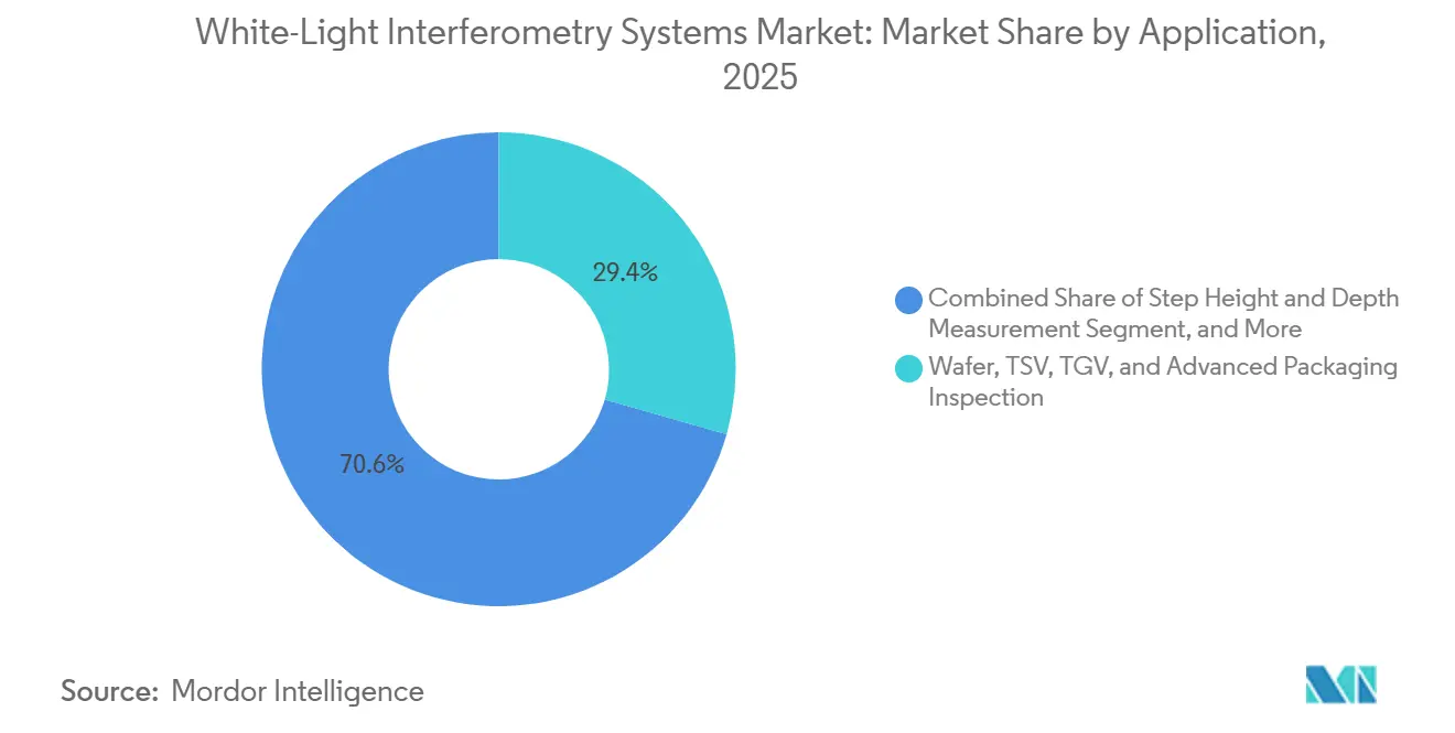
- By application, Wafer, TSV, TGV, and Advanced Packaging Inspection accounted for 29.43% of the white-light interferometry systems market in 2025 and are projected to expand at an 8.44% CAGR through 2031.
- By end-user industry, semiconductor and electronics held 36.74% revenue share in 2025 and is projected to expand at an 8.28% CAGR through 2031.
- By geography, Asia-Pacific held 41.86% of global revenue in 2025 and is projected to expand at an 8.59% CAGR through 2031.
Note: Market size and forecast figures in this report are generated using Mordor Intelligence’s proprietary estimation framework, updated with the latest available data and insights as of January 2026.
Global White-Light Interferometry Systems Market Trends and Insights
Drivers Impact Analysis*
| Driver | (~) % Impact on CAGR Forecast | Geographic Relevance | Impact Timeline |
|---|---|---|---|
| Advanced Semiconductor Node Migration | +2.5% | Global, concentrated in Asia-Pacific, Taiwan, South Korea, Japan, and North America | Short term (≤ 2 years) |
| Expansion of Wafer-Level Packaging and MEMS Manufacturing | +1.8% | Asia-Pacific core, with expansion into North America and Europe | Medium term (2-4 years) |
| Demand for Non-Contact Nanometer-Scale Surface Measurement | +1.3% | Global | Medium term (2-4 years) |
| Integration of Inline Metrology With Automated Production | +1.0% | Asia-Pacific core, with expansion into North America and Europe | Medium term (2-4 years) |
| AI-Assisted Defect Classification and Recipe Optimization | +0.8% | Global, with early gains in North America and Asia-Pacific | Short term (≤ 2 years) |
| Distributed Calibration Data for Cross-Site Metrology Consistency | +0.4% | Global, concentrated in multi-site foundries | Long term (≥ 4 years) |
| Source: Mordor Intelligence | |||
Advanced Semiconductor Node Migration
The shift toward 2 nm and smaller process nodes is increasing the need for surface measurement tools. Gate-all-around nanosheet designs add stacked structures and backside power delivery features. These features require non-destructive characterization during repeated process qualification cycles. TSMC reported that its N2 node had 1.5 times more tape-outs than its 3 nm predecessor by mid-2025.[1]Taiwan Semiconductor Manufacturing Company, “Investor Communications and Capital Expenditure Guidance,” Taiwan Semiconductor Manufacturing Company, investor.tsmc.com. Each tape-out can add further surface characterization work before volume production. Coherence scanning interferometry can measure complex vertical structures without contacting the wafer. The white-light interferometry systems market therefore benefits from node complexity, even when wafer unit growth is less pronounced.
Expansion of Wafer-Level Packaging and MEMS Manufacturing
Wafer-level packaging and MEMS production are raising measurement requirements for inline surface tools. Hybrid bonding depends on tightly controlled copper pad topography before wafers are joined. A 2025 study reported a 0.79 nm standard deviation across 20 consecutive WLI measurements on hybrid bonding copper-pad surfaces.[2]Huy Hoang Chu et al., “Nanometer-Resolution White-Light Scanning Interferometry for Surface-Profiling of Hybrid Bonding Samples for Advanced Semiconductor Packaging,” Applied Surface Science, sciencedirect.com. The study found stronger performance than confocal laser scanning microscopy on the tested specimens. Copper dishing limits in HBM hybrid bonding can fall below 1 nm. Non-contact interferometry can confirm compliance without creating surface damage. This requirement supports wider use of WLI in packaging lines and MEMS manufacturing.
Demand for Non-Contact Nanometer-Scale Surface Measurement
Manufacturers in precision engineering, medical devices, and optics are tightening surface roughness requirements. Surface roughness below 10 nm Ra can be difficult to assess with stylus methods. Stylus contact can create sample damage and tip-convolution errors on small features. A 2026 study demonstrated Fourier ptychographic coherence scanning interferometry on 300 µm-deep micro-trenches with a 30:1 aspect ratio. The method retained diffraction-limited lateral resolution in geometries that challenge confocal techniques. A separate study reported 0.258 nm repeatability across a 1 mm range using frequency-comb-referenced multiwavelength interferometry. These capabilities extend the white-light interferometry systems market into aerospace and life-science measurement tasks.
Integration of Inline Metrology With Automated Production
High-volume fabs are moving from sampled measurement toward 100% inline inspection. This change is particularly important at sub-3 nm nodes, where measurement delays can affect yield response. Bruker designed its InSight WLI for inline 3D profilometry on 200 mm and 300 mm wafers.[3]Bruker Corporation, “InSight WLI, Inline 3D Optical Profilometry for Semiconductor Manufacturing,” Bruker Corporation, bruker.com. The system supports SECS/GEM connectivity and includes more than 35 built-in analyses. Full-die 3D maps can create large daily data volumes at wafer-level measurement frequency. A 2026 conference paper reported a 2-fold throughput improvement using AI spectral reconstruction for inline measurement.[4]GlobalFoundries and IEEE, “Accelerating XPS Metrology With AI to Enhance Throughput in High-Volume Semiconductor Manufacturing,” IEEE Advanced Semiconductor Manufacturing Conference, ieee.org. These conditions increase demand for integrated measurement and analytics systems.
Restraints Impact Analysis*
| Restraint | (~) % Impact on CAGR Forecast | Geographic Relevance | Impact Timeline |
|---|---|---|---|
| High Capital Expenditure for Advanced WLI Systems | -1.5% | Global, most acute in emerging semiconductor markets | Short term (≤ 2 years) |
| Competition From Confocal, Focus-Variation, and Atomic Force Microscopy | -1.0% | Global | Medium term (2-4 years) |
| Vibration Sensitivity in Production Environments | -0.5% | Global, most acute in high-throughput fabs | Short term (≤ 2 years) |
| Shortage of Certified Reference Artifacts and Interferometric Objectives | -0.3% | Global | Medium term (2-4 years) |
| Source: Mordor Intelligence | |||
High Capital Expenditure for Advanced WLI Systems
Production-grade WLI systems can cost low single-digit USD millions per tool. This investment level concentrates purchases among large fabs and outsourced semiconductor assembly and test providers. Smaller manufacturers and research institutions can face more difficult purchase decisions. The barrier is most visible in South America, Southeast Asia, and Africa. Sub-micron interferometric objectives can also cost tens of thousands of USD. Custom optical designs can lengthen delivery schedules for emerging process requirements. Modular platforms help customers add capability in stages, but they do not remove the initial capital threshold in the white-light interferometry systems market.
Competition From Confocal, Focus-Variation, and Atomic Force Microscopy
WLI competes with several established methods in specialized measurement tasks. Confocal microscopy can deliver strong lateral resolution on complex surfaces. It has gained use in ophthalmic lenses and medical device finishing. Focus-variation microscopy can measure steep flanks that challenge WLI with standard numerical apertures. This makes it useful for cutting-tool inspection. Atomic force microscopy retains a leading role in sub-nanometer hybrid bonding pad characterization, despite lower throughput. Park Systems combines AFM and WLI in its NX-Hybrid platform for automation-compatible measurement. Hybrid configurations can broaden capability, although they also add cost and operating complexity.
*Our forecasts treat driver/restraint impacts as directional, not additive. The impact forecasts reflect baseline growth, mix effects, and variable interactions.
Segment Analysis
By Product Type: Inline Systems Change Process Control Economics
Benchtop and Laboratory Systems held 46.83% of product-type revenue in 2025. Their role remains important for recipe development, failure analysis, and material qualification. These systems can use configurable objectives and vibration-isolated stages. They also provide large working envelopes for varied samples. Fab research centers use them for process development before manufacturing release. Floor-Standing Systems serve heavy samples and large-format inspection tasks. Aerospace parts and precision optics require stable scan paths during these measurements. Portable and Handheld Systems remain a smaller category for field quality audits.
Inline and On-Machine Systems are projected to expand at an 8.46% CAGR through 2031. The white-light interferometry systems market size for this category benefits from shorter feedback loops on production lines. A 2025 study demonstrated active wavefront-compensatory coherence scanning interferometry on buried microstructures. It achieved 0.95 µm lateral resolution below encapsulating layers between 100 µm and 300 µm thick. The approach supports inspection of encapsulated MEMS and stacked-die structures. Zygo introduced its ZeGage Pro with SureScan vibration resistance for floor-level installation. This design addresses a practical barrier in high-vibration production areas. Automotive stamping and medical implant inspection can also use portable systems for periodic quality checks.



By Technology: AI-Enabled Analysis Supports Measurement Intelligence
Coherence Scanning Interferometry held 44.67% of technology revenue in 2025. This method covers a wide range of surfaces in the white-light interferometry systems market. It is used for MEMS membranes, semiconductor interconnects, optical flats, and bearing races. Its vertical range supports applications with different material surfaces and feature heights. Vertical Scanning Interferometry retains an important role in smooth optical surface measurement. Phase-Shifting Interferometry supports laser optics and telescope mirror qualification. Low-Coherence Thickness Measurement serves transparent thin-film stacks. These methods remain complementary within laboratory and production workflows.
AI-Enabled Interferometric Analysis is projected to expand at an 8.37% CAGR through 2031. The white-light interferometry systems market size for AI-supported tools reflects demand for faster processing without lower spatial resolution. A 2025 study found that algorithmic signal processing reduced WLI measurement time on wafer-scale high-aspect-ratio structures. The study preserved the required spatial resolution. Software can allow similar hardware to serve higher-value applications. This reduces upgrade costs for installed systems. Vendors have shifted more development resources toward analytics platforms since 2025. AI-assisted recipe optimization is becoming more common in new system releases.
By Application: Advanced Packaging Inspection Supports Demand
Wafer, TSV, TGV, and Advanced Packaging Inspection held 29.43% of application revenue in 2025. It is projected to expand at an 8.44% CAGR through 2031. This application held the largest white-light interferometry systems market share and the highest reported application growth rate. CoWoS, SoIC, hybrid bonding, and fan-out wafer-level packaging require topography verification at bonding interfaces. Each process places greater emphasis on non-contact measurement of surface condition. ISO 25178-2 supports areal surface texture measurement practices. NIST provides SRM 1732 traceability for silicon nitride film thickness measurement. These reference materials support consistent calibration and verification practices.
Surface Roughness and Texture Measurement remains the largest application by volume. Step Height and Depth Measurement supports photolithography process control. Defect Review and Failure Analysis helps preserve sample integrity during yield investigation. Thin-Film and Coating Thickness Measurement is gaining use for transparent oxide and nitride stacks. Low-coherence methods can supplement reflectometry when spectral model accuracy is limited. Flatness, Form, and Parallelism Measurement is important for turbine components and hydraulic seals. Other applications include academic work in materials science and photonics. These demand areas are influenced by research funding and equipment access.
By End-User Industry: Semiconductor Demand Reflects Node Complexity
The semiconductor and electronics segment held 36.74% of end-user revenue in 2025. It is projected to expand at an 8.28% CAGR through 2031. This segment leads both reported end-user share and growth. The white-light interferometry systems market share reflects demanding process control at 2 nm-class nodes. Processed wafers at these nodes can cost more than USD 20,000. Better surface measurement can improve yield and support the value case for inspection tools. Advanced packaging also creates additional measurement points during assembly. These conditions sustain demand across leading foundries and memory producers.
Precision Manufacturing held the second-largest end-user share. Its applications include aerospace finishing, cutting-tool wear monitoring, and mold qualification. Production-compatible WLI systems are replacing tactile profilometers in selected tasks. Automotive and aerospace users measure powertrain components and hydraulic seals. Electric drivetrain durability requirements are tightening roughness verification needs. Medical Devices and Life Sciences use non-destructive measurement for implant and ophthalmic lens production. Optics and Photonics users measure AR waveguides, laser optics, and telescope mirrors. Research and Academia continues to use benchtop systems for materials science and MEMS work.
Geography Analysis
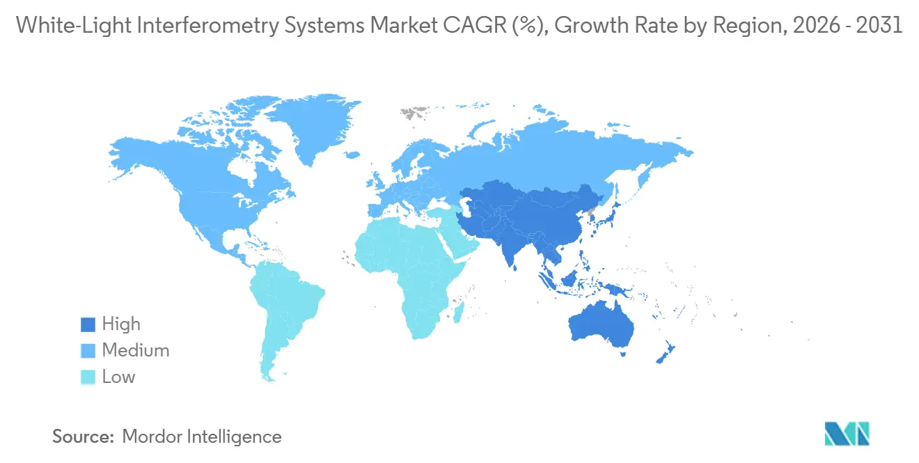
Asia-Pacific held 41.86% of global revenue in 2025. The region is projected to expand at an 8.59% CAGR through 2031. This represented the largest white-light interferometry systems market share and the highest regional growth rate. Taiwan supports demand through 2 nm foundry ramp-ups. South Korea supports demand through HBM and hybrid bonding quality control. China is increasing domestic semiconductor equipment development. Japan remains relevant for automotive MEMS, optical systems, and equipment sub-assembly verification. These markets combine leading-edge manufacturing with a growing need for packaging inspection.
North America was the second-largest geography in 2025. Advanced packaging investments at TSMC Arizona and Intel facilities support regional equipment demand. Defense and aerospace programs also require precision optics manufacturing. These applications need high-precision surface and form measurement. Europe concentrates demand in Germany, the Netherlands, and France. Germany combines precision instrument suppliers with automotive Tier-1 manufacturing. The Netherlands benefits from optical metrology demand tied to the ASML supply chain. France benefits from semiconductor research activity around CEA-Leti.
South America, the Middle East and Africa, and the rest of Asia-Pacific form smaller demand pools. Brazil leads South American demand through automotive component manufacturing. Saudi Arabia and the UAE are investing in advanced manufacturing capability. Early WLI installations support aerospace maintenance, repair, and overhaul metrology laboratories. African demand is concentrated in academic institutions and South Africa's engineering metrology sector. New fab investments under the Chips and Science Act and the European Chips Act can support equipment demand in Arizona, Germany, and Japan. The white-light interferometry systems market has opportunities where new facilities need qualified process control tools.

Competitive Landscape
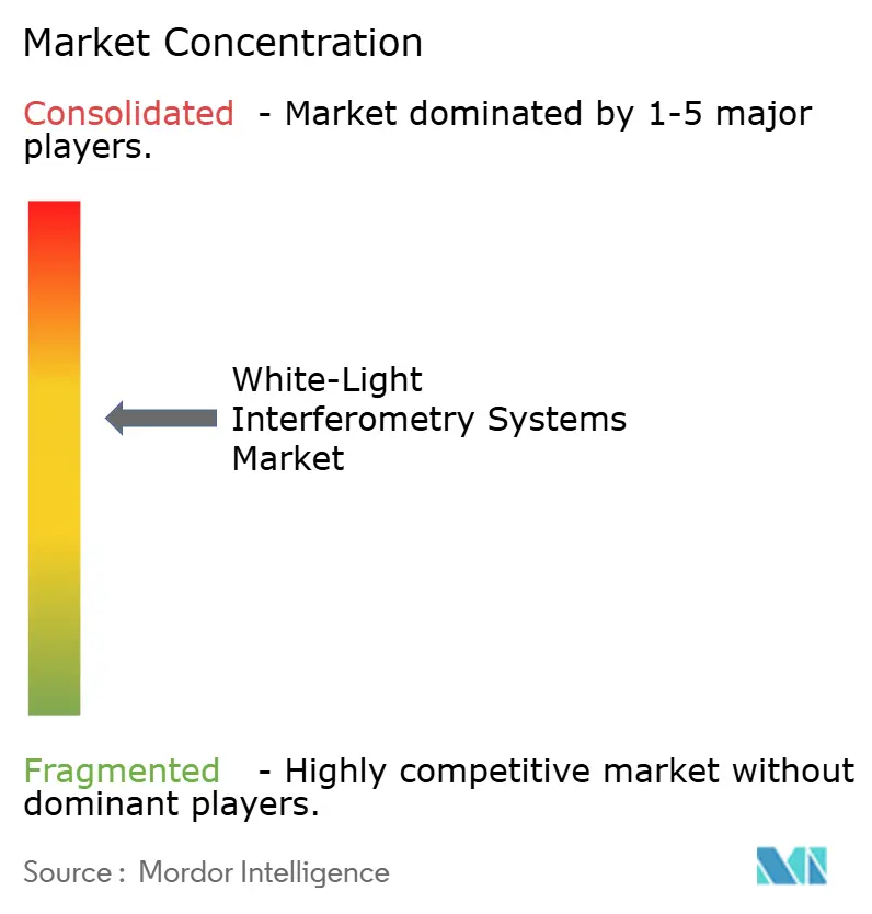
The white-light interferometry systems market is moderately consolidated, with AMETEK through Zygo, Bruker Corporation, KLA Corporation, and Keyence Corporation holding an important combined position, while Sensofar Metrology, Taylor Hobson, Mahr GmbH, and Polytec GmbH retain established roles in application-specific niches that need particular optical configurations, established local support, or experience with a defined surface measurement workflow. The competitive basis has shifted beyond core hardware specifications because semiconductor and precision-manufacturing buyers increasingly consider automation depth, software capability, data handling, and the ability to connect measurement results to a corrective production action, especially where surface variation can affect yield, bonding quality, or final optical performance. KLA reported USD 12.16 billion in FY2025 revenue and stated that advanced packaging process control exceeded USD 925 million in application revenue, which indicates the scale of capital investment directed toward process-control applications that include complex surface measurement needs. For suppliers in the white-light interferometry systems market, the relevant commercial question is whether a platform can create reliable metrology feedback during a production cycle, rather than simply deliver an isolated measurement result, because fabs favor systems that can fit into established process-control routines and provide usable data to manufacturing engineers without lengthy manual interpretation.
Zygo has continued to build its position through coherence scanning interferometry and laser interferometry products, and its April 2026 presentation of the Nexview NX2 3D optical profiler and Qualifire 1.2 laser interferometer showed continued attention to users operating across both laboratory and production environments. The continued development of these platforms matters because semiconductor, optical manufacturing, precision engineering, aerospace, and medical device users have different sample sizes, throughput expectations, and surface characteristics, which makes configuration flexibility a practical part of vendor selection and helps established suppliers serve more than one end-use setting with related measurement technology. Bruker has also pursued adjacent measurement capability through its 2026 photothermal AFM-IR spectroscopy initiative, a move that expands the technical range around its core installed base and can help the company address customer requirements that combine surface measurement with other forms of material characterization. This strategy reflects the fact that many buyers do not select a surface measurement system in isolation, since their broader workflow can include failure analysis, material qualification, substrate review, packaging process control, and production integration, all of which increase the value of vendors able to connect WLI with related analytical tools and service capabilities.
Keyence acquired CADENAS GmbH in 2025, strengthening its digital engineering ecosystem and smart-factory workflow integration, while regional companies such as SFA and Park Systems have entered or expanded in applications connected with HBM, hybrid bonding, glass substrates, and automation-compatible measurement platforms where close alignment with chipmaker requirements can be important. The white-light interferometry systems market is therefore divided between global companies that compete on product breadth, compliance support, installed-base relationships, and international service coverage, and regional specialists that compete on application fit, faster response to packaging changes, and close access to semiconductor customers that are developing new manufacturing steps. Inline WLI with AI-supported recipe optimization represents an opening in advanced packaging fabs because the measurement requirement is clear, yet deployments can still need substantial SECS/GEM engineering before production data can be used effectively within a fab's existing automation environment, creating a need for suppliers that can simplify implementation as well as improve measurement capability. Alternative technologies remain relevant in this competitive setting, with confocal systems serving certain complex surfaces, focus-variation systems supporting steep-flank inspection, and atomic force microscopy retaining a role where sub-nanometer vertical accuracy is needed, which means WLI suppliers must continue to explain their relative strengths in throughput, non-contact operation, vertical range, and compatibility with production use. FARO Technologies is not a direct participant because its portfolio centers on 3D laser scanning, portable CMM arms, and laser trackers for large-scale dimensional measurement, while HORIBA is not a direct participant because it does not offer WLI surface profilometry systems, leaving Onto Innovation and Veeco Instruments as more relevant adjacent suppliers for advanced packaging inspection and surface characterization tasks.
White-Light Interferometry Systems Industry Leaders
AMETEK, Inc.
Bruker Corporation
KLA Corporation
Keyence Corporation
Polytec GmbH
- *Disclaimer: Major Players sorted in no particular order

Recent Industry Developments
- May 2026: Zygo showcased the Nexview NX2 3D optical profiler and Qualifire 1.2 laser interferometer at Optatec 2026 in Frankfurt, Germany, from May 5-7, targeting laboratory and production environments in optical manufacturing and precision engineering.
- March 2026: Keyence Corporation launched the VK-X4000 Series 3D Optical Profiling Microscope, extending its high-resolution surface characterization portfolio with expanded analytical capabilities for precision manufacturing and semiconductor quality control.
- January 2026: Zygo presented its integrated precision metrology portfolio, including the Qualifire laser interferometer family, at SPIE Photonics West 2026, emphasizing applicability across semiconductor, life sciences, aerospace, and medical device applications.
- August 2025: Park Systems unveiled an expanded FX Large Sample AFM series at SEMICON Korea 2025, including the FX300 for 300 mm wafer analysis and FX200 IR and FX300 IR variants with integrated infrared spectroscopy, extending hybrid WLI-AFM metrology capabilities to large-format advanced packaging substrates.


Global White-Light Interferometry Systems Market Report Scope
The White-Light Interferometry Systems Market covers non-contact optical metrology instruments that use low-coherence (broadband) white-light interference to measure 3D surface topography, roughness, step height, thin-film thickness, and micro-scale features with nanometer-level vertical resolution.
The White-Light Interferometry Systems Market Report is Segmented by Product Type (Benchtop and Laboratory Systems, Floor-Standing Systems, Inline and On-Machine Systems, and Portable and Handheld Systems), Technology (Coherence Scanning Interferometry, Vertical Scanning Interferometry, Phase-Shifting Interferometry, Low-Coherence Thickness Measurement, and AI-Enabled Interferometric Analysis), Application (Surface Roughness and Texture Measurement, Step Height and Depth Measurement, Flatness, Form, and Parallelism Measurement, Thin-Film and Coating Thickness Measurement, Wafer, TSV, TGV, and Advanced Packaging Inspection, Defect Review and Failure Analysis, and Other Applications), End-User (Semiconductor and Electronics, Precision Manufacturing, Automotive and Aerospace, Medical Devices and Life Sciences, Optics and Photonics, Research and Academia, and Other End-User Industry), and Geography (North America, South America, Europe, Asia-Pacific, and Middle East and Africa). The Market Forecasts are Provided in Terms of Value (USD).
| Benchtop and Laboratory Systems |
| Floor-Standing Systems |
| Inline and On-Machine Systems |
| Portable and Handheld Systems |
| Coherence Scanning Interferometry |
| Vertical Scanning Interferometry |
| Phase-Shifting Interferometry |
| Low-Coherence Thickness Measurement |
| AI-Enabled Interferometric Analysis |
| Surface Roughness and Texture Measurement |
| Step Height and Depth Measurement |
| Flatness, Form, and Parallelism Measurement |
| Thin-Film and Coating Thickness Measurement |
| Wafer, TSV, TGV, and Advanced Packaging Inspection |
| Defect Review and Failure Analysis |
| Other Applications |
| Semiconductor and Electronics |
| Precision Manufacturing |
| Automotive and Aerospace |
| Medical Devices and Life Sciences |
| Optics and Photonics |
| Research and Academia |
| Other End-User Industry |
| North America | United States | |
| Canada | ||
| Mexico | ||
| South America | Brazil | |
| Argentina | ||
| Rest of South America | ||
| Europe | Germany | |
| United Kingdom | ||
| France | ||
| Italy | ||
| Spain | ||
| Rest of Europe | ||
| Asia-Pacific | China | |
| Japan | ||
| India | ||
| South Korea | ||
| ASEAN | ||
| Rest of Asia-Pacific | ||
| Middle East and Africa | Middle East | Saudi Arabia |
| United Arab Emirates | ||
| Turkey | ||
| Rest of the Middle East | ||
| Africa | South Africa | |
| Nigeria | ||
| Rest of Africa | ||
| By Product Type | Benchtop and Laboratory Systems | ||
| Floor-Standing Systems | |||
| Inline and On-Machine Systems | |||
| Portable and Handheld Systems | |||
| By Technology | Coherence Scanning Interferometry | ||
| Vertical Scanning Interferometry | |||
| Phase-Shifting Interferometry | |||
| Low-Coherence Thickness Measurement | |||
| AI-Enabled Interferometric Analysis | |||
| By Application | Surface Roughness and Texture Measurement | ||
| Step Height and Depth Measurement | |||
| Flatness, Form, and Parallelism Measurement | |||
| Thin-Film and Coating Thickness Measurement | |||
| Wafer, TSV, TGV, and Advanced Packaging Inspection | |||
| Defect Review and Failure Analysis | |||
| Other Applications | |||
| By End-User Industry | Semiconductor and Electronics | ||
| Precision Manufacturing | |||
| Automotive and Aerospace | |||
| Medical Devices and Life Sciences | |||
| Optics and Photonics | |||
| Research and Academia | |||
| Other End-User Industry | |||
| By Geography | North America | United States | |
| Canada | |||
| Mexico | |||
| South America | Brazil | ||
| Argentina | |||
| Rest of South America | |||
| Europe | Germany | ||
| United Kingdom | |||
| France | |||
| Italy | |||
| Spain | |||
| Rest of Europe | |||
| Asia-Pacific | China | ||
| Japan | |||
| India | |||
| South Korea | |||
| ASEAN | |||
| Rest of Asia-Pacific | |||
| Middle East and Africa | Middle East | Saudi Arabia | |
| United Arab Emirates | |||
| Turkey | |||
| Rest of the Middle East | |||
| Africa | South Africa | ||
| Nigeria | |||
| Rest of Africa | |||


Key Questions Answered in the Report
What is the size of the white-light interferometry systems market?
The white-light interferometry systems market was valued at USD 290.54 million in 2025 and is estimated at USD 310.52 million in 2026. It is forecast to reach USD 457.68 million by 2031 at an 8.07% CAGR.
What is driving demand for white-light interferometry systems?
Advanced semiconductor nodes, hybrid bonding, wafer-level packaging, MEMS production, and inline measurement needs support demand.
Which product category is expanding fastest?
Inline and On-Machine Systems are projected to expand at an 8.46% CAGR through 2031 as fabs seek faster process feedback.
Which application leads white-light interferometry demand?
Wafer, TSV, TGV, and Advanced Packaging Inspection held 29.43% of application revenue in 2025 and is projected to expand at an 8.44% CAGR.
Which region has the strongest position in white-light interferometry systems?
Asia-Pacific held 41.86% of global revenue in 2025 and is projected to expand at an 8.59% CAGR through 2031.
What limits adoption of white-light interferometry systems?
High capital costs, vibration sensitivity, limited reference artifacts, and competing confocal, focus-variation, and atomic force microscopy methods can limit adoption.
Page last updated on: