Wafer Cleaning Equipment Market Size and Share
Market Overview
| Study Period | 2019 - 2030 |
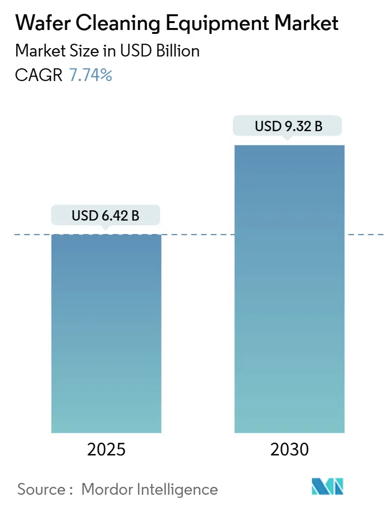
| Market Size (2025) | USD 6.42 Billion |
| Market Size (2030) | USD 9.32 Billion |
| Growth Rate (2025 - 2030) | 7.74% CAGR |
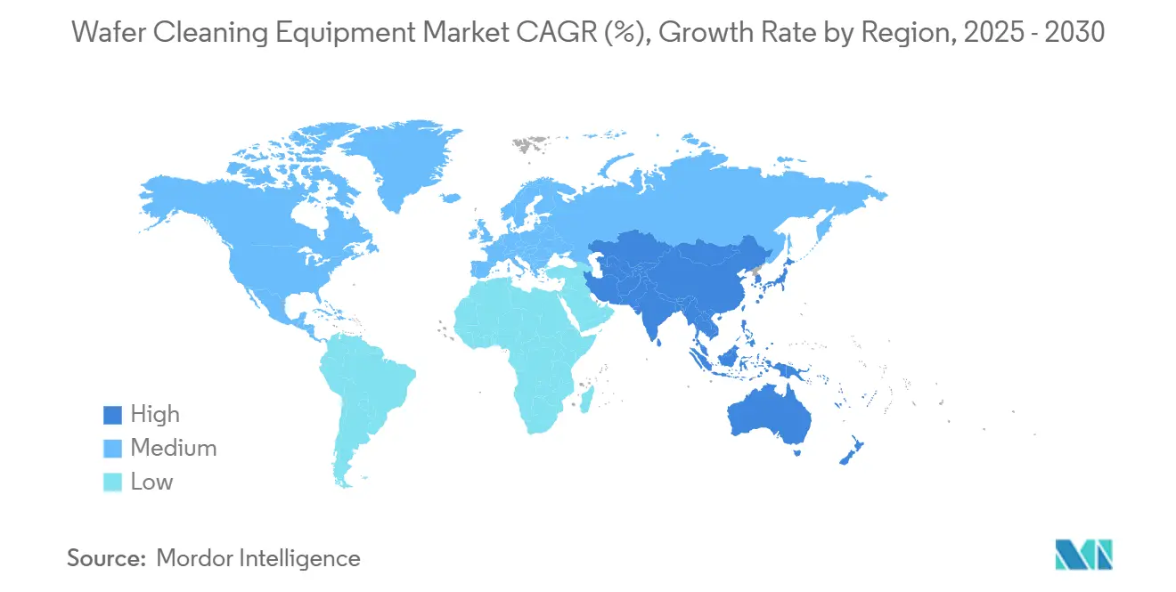
| Fastest Growing Market | Asia Pacific |
| Largest Market | Asia Pacific |
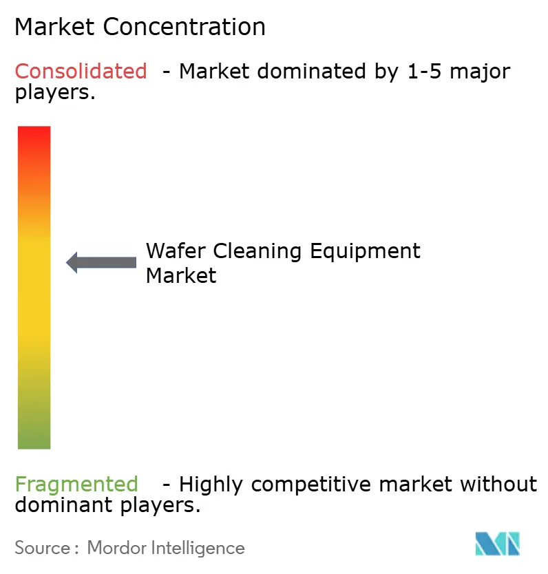
| Market Concentration | Medium |
Major Players*Disclaimer: Major Players sorted in no particular order Image © Mordor Intelligence. Reuse requires attribution under CC BY 4.0. |
|
Wafer Cleaning Equipment Market Analysis by Mordor Intelligence
The wafer cleaning equipment market size stood at USD 6.42 billion in 2025 and is forecast to reach USD 9.32 billion by 2030, reflecting a 7.74% CAGR during 2025-2030. The expansion mirrors the semiconductor industry’s move toward 1.6 nm process technology, where sub-10 nm particle removal becomes mandatory.[1]Tokyo Electron, “Cryogenic Etching – Tokyo Electron’s ‘Digital and Green Transformation’ of Semiconductor Process Equipment,” tel.com EUV lithography adoption, foundry capacity build-outs in Taiwan, South Korea, China, and the United States, and the transition to 300 mm silicon-carbide and gallium-nitride wafers are amplifying demand across the wafer cleaning equipment market. Environmental mandates targeting fluorinated greenhouse gases and rising ultrapure-water costs are reshaping equipment selection criteria, but suppliers offering water-efficient or cryogenic solutions are capturing share. Competitive intensity remains moderate because sophisticated process know-how, long qualification cycles, and service footprints act as barriers to entry.
Key Report Takeaways
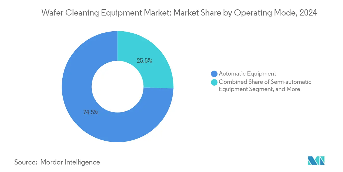
- By operating mode, fully automatic systems led with 74.5% of wafer cleaning equipment market share in 2024; the same segment is projected to post the fastest 8.5% CAGR to 2030.
- By technology type, single-wafer spray tools commanded 33.2% revenue share in 2024, while single-wafer cryogenic systems are forecast to expand at a 12.2% CAGR through 2030.
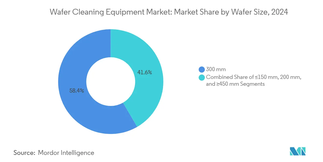
- By wafer size, 300 mm tools accounted for 58.4% of the wafer cleaning equipment market size in 2024; ≥450 mm solutions are expected to accelerate at a 19.5% CAGR between 2025-2030.
- By application, memory devices captured 30.2% share of the wafer cleaning equipment market size in 2024; power discrete and IC devices are set to grow at 13.5% CAGR to 2030.
- By end-user, pure-play foundries represented 43.3% demand in 2024, whereas OSAT providers are anticipated to register the quickest 9.2% CAGR through 2030.
- By geography, Asia-Pacific held 72.5% revenue in 2024 and is advancing at 14.3% CAGR to 2030.
Global Wafer Cleaning Equipment Market Trends and Insights
Drivers Impact Analysis
| Driver | (~) % Impact on CAGR Forecast | Geographic Relevance | Impact Timeline |
|---|---|---|---|
| Proliferation of 3-D NAND and DRAM node shrinks driving defect-free FEOL cleaning demand | +2.1% | Global, concentrated in Asia-Pacific memory hubs | Medium term (2-4 years) |
| Foundry capacity expansion in the U.S., Korea and Taiwan creating new tool install base | +1.8% | North America, Asia-Pacific core markets | Short term (≤ 2 years) |
| Transition toward 300 mm SiC and GaN power wafers requiring new wet-bench chemistries | +1.4% | Global, early adoption in automotive regions | Long term (≥ 4 years) |
| Adoption of EUV lithography necessitating ultra-low particle cleans <10 nm | +1.6% | Advanced foundry markets globally | Medium term (2-4 years) |
| Rapid fab investments by Chinese IDMs despite U.S. export controls | +0.9% | China mainland, spillover to Southeast Asia | Short term (≤ 2 years) |
Source: Mordor Intelligence
Proliferation of 3-D NAND and DRAM Node Shrinks Driving Defect-Free FEOL Cleaning Demand
Mass-production roadmaps toward 1,000-layer 3-D NAND by 2030 multiply cleaning steps because every additional layer increase particle-induced yield loss. SK Hynix earmarked USD 75 billion for memory scaling through 2028, directing 80% to high-bandwidth memory. Lam Research introduced Cryo 3.0 etch to mitigate polymer residues in deep trenches. Equipment makers that deliver sub-angstrom removal precision are benefiting from rising layer counts, lifting the wafer cleaning equipment market. Memory fabs now contractually link tool purchase decisions to demonstrated removal efficiency below 10 nm, reinforcing long-term demand.
Foundry Capacity Expansion in the U.S., Korea and Taiwan Creating New Tool Install Base
The CHIPS Act triggered large-scale tool procurement in Arizona, where TSMC’s complex requires thousands of process tools. Samsung and SK Hynix committed 622 trillion won (USD 471 billion) for 16 new fabs by 2047, intensifying immediate order cycles. Tokyo Electron nearly doubled R&D spend to JPY 1.5 trillion over five years to secure next-generation opportunities. Capacity additions focus on 3 nm and below, translating to tool specs that only advanced wafer cleaning equipment market participants can meet. Short tool lead-times and service proximity drove an immediate surge in orders for fully automatic cleaning platforms.
Transition Toward 300 mm SiC and GaN Power Wafers Requiring New Wet-Bench Chemistries
Electric-vehicle traction inverters and solar inverters favored 300 mm SiC substrates that demand abrasive-particle removal without crystal damage. Infineon released its first 200 mm SiC products, validating the scaling pathway. Scientific studies identified new slurry formulations for SiC chemical-mechanical polishing. Cleaning vendors had to redesign bath materials and integrate particle-free rinse modules, propelling long-cycle replacement demand in the wafer cleaning equipment market. Automotive OEM qualification cycles are long, reinforcing sustained tool utilization once installed.
Adoption of EUV Lithography Necessitating Ultra-Low Particle Cleans <10 nm
High-NA EUV scanners priced at about USD 380 million each compel fabs to eliminate once acceptable particles. Intel processed 30,000 wafers with its first two High-NA machines, proving the need for extreme cleanliness. ASML requires pre-exposure particle levels below detection thresholds, forcing cleaning platforms to deliver better than ISO 1 performance. Tokyo Electron’s monopoly in EUV resist coating spurred complementary demand for compatible cleaners that maintain defect density well below 0.05 cm². Each scrapped 3 nm wafer costs USD 18,000, aligning ROI firmly with advanced cleaning adoption.
Restraints Impact Analysis
| Restraint | (~) % Impact on CAGR Forecast | Geographic Relevance | Impact Timeline |
|---|---|---|---|
| Stringent discharge regulations on fluorinated greenhouse gases (F-GHGs) | -1.2% | Global, stricter enforcement in EU and North America | Medium term (2-4 years) |
| Rising ultrapure water (UPW) cost in drought-prone semiconductor hubs | -0.8% | Water-stressed regions: Arizona, Taiwan, California | Short term (≤ 2 years) |
| High capex intensity versus alternative dry plasma cleans in BEOL | -0.6% | Cost-sensitive markets and mature node production | Long term (≥ 4 years) |
Source: Mordor Intelligence
Stringent Discharge Regulations on Fluorinated Greenhouse Gases (F-GHGs)
The global semiconductor industry pledged to phase out PFOA, tightening chemical options. The U.S. EPA’s accelerated PFAS review injects uncertainty into chemistry roadmaps. European fabs cut PFC emissions 42% from 2010-2020, mainly by retrofitting abatement modules. Equipment firms now bundle scrubbers and closed-loop chemical recycle units, raising acquisition cost and extending ROI timelines, moderating the wafer cleaning equipment market growth projection.
Rising Ultrapure-Water (UPW) Cost in Drought-Prone Semiconductor Hubs
Advanced cleaning recipes for 16 nm and below consumed over 35% more water per wafer, inflating operating costs. TSMC’s Arizona fab attracted scrutiny because the region faces long-term drought risk despite official assurances. Intel aimed for net-positive water by 2030 with large reclamation programs. Rising UPW tariffs incentivize single-wafer spray and cryogenic CO₂ tools that cut rinse volumes by up to 90%, reshaping vendor selection criteria in the wafer cleaning equipment market.
Segment Analysis
By Operating Mode: Automation Drives Precision and Throughput
Fully automatic platforms generated 74.5% of 2024 revenue thanks to strict contamination-control mandates on advanced logic lines, placing the wafer cleaning equipment market in an automation-first paradigm. Semi-automatic tools persisted in R&D cleanrooms, while manual systems stayed limited to specialty or legacy flows. The fully automatic segment, already dominant, is forecast to compound at 8.5% annually on the back of AI-driven recipe optimization. SCREEN’s SS-3200 spin-scrubber processed 500 wafers per hour while cutting deionized-water use, underpinning replacement cycles.[2]SCREEN Semiconductor Solutions, “Launch of 200 mm Wafer Cleaning System,” screen.co.jp
Process analytics embedded in machine controllers now store millions of datapoints per lot, allowing fabs to predict excursions and prevent line stops. Vendors embed predictive-maintenance modules that flag nozzle fouling or flow instability. These digital workflows align with smart-manufacturing mandates, supporting premium pricing. Consequently, the wafer cleaning equipment market sees purchasing decisions shift from capex alone toward total cost-of-ownership anchored in uptime metrics and water savings.
By Technology Type: Single-Wafer Solutions Lead Innovation
Single-wafer spray lines earned 33.2% revenue share in 2024 by combining small footprint, chemistry savings, and recipe flexibility, helping maintain the wafer cleaning equipment market trajectory. Cryogenic CO₂ variants, though newer, registered the fastest 12.2% CAGR outlook on the promise of near-zero liquid discharge. Batch immersion tools survived in high-volume commodity lines, while batch spray occupied the mid-tier. Scrubbers served blanket oxide removal tasks that chemicals alone could not address.
Tokyo Electron’s cryogenic etch reduced CO₂ emissions 80%, validating green-chemistry claims. ACM Research’s Ultra C Tahoe slashed sulfuric-acid use 75% while matching legacy performance, winning multiple foundry installs. Technology decisions now revolve around water and greenhouse-gas metrics as much as particle-count specs, reinforcing the strategic importance of single-wafer innovation to the wafer cleaning equipment market.
By Wafer Size: 300 mm Dominance with 450 mm Emergence
The 300 mm format accounted for 58.4% of 2024 revenue, forming the cornerstone of the wafer cleaning equipment market. Tools rated for ≥450 mm wafers are expected to surge 19.5% CAGR because larger substrates promise cost per die reductions at 2 nm nodes. Power devices on 200 mm SiC remain essential to EV drivetrains, sustaining demand for dual-format platforms. Legacy ≤150 mm lines persisted in the photonics and research segments.
Infineon’s 200 mm SiC ramp showed that material hardness drives higher brush-scrub torque requirements. Meanwhile, toolmakers prototype full-wafer-thickness support frames for 450 mm to avoid warpage, complicating megasonic rinse module design. Given wafer price differentials—3 nm wafers at USD 18,000 versus USD 5,000 for 28 nm—fabs see economics favoring platform upgrades.
By Application: Memory Devices Drive Advanced Cleaning Requirements
Memory lines generated 30.2% demand in 2024 as 3-D NAND structures imposed intricate clean-etch-clean loops that stretch over 900 process steps. Power discrete and IC lines show the steepest 13.5% CAGR on EV and renewable energy scale-up. Smartphone/tablet SoCs continued to underpin baseline volumes, while RF modules and CMOS image sensors drove niche contamination specs for high-frequency or optical performance.
Samsung’s R&D complex introduced wafer-to-wafer bonding, elevating post-bond clean needs for heterogeneous integration. Automotive OEM reliability mandates—15-year lifetimes at extreme temperatures—tightened ionic contamination limits, pushing demand for advanced single-wafer spray tools. These factors anchor application-led diversification inside the wafer cleaning equipment market.
By End-User: Pure-Play Foundries Lead Equipment Adoption
Pure-play foundries accounted for 43.3% of 2024 orders because customers spanning AI accelerators to mobile chipsets rely on standardized cleanliness. OSAT houses are projected to outpace at 9.2% CAGR as advanced packaging requires void-free surfaces prior to bonding. IDMs split capex between internal fabs and external capacity, ensuring multi-sourcing of cleaning platforms.
ACM Research grew 40% to USD 782.1 million by expanding Chinese foundry installs, especially at 28 nm and below. Taiwan Speciality Chemicals’ purchase of Hung Jie Technology widened dry-clean service coverage for OSAT customers. The wafer cleaning equipment market, hence, aligns closely with capacity localization and backend value-chain shifts.
Geography Analysis
Asia-Pacific generated 72.5% of 2024 revenue, anchored by cluster investments in Taiwan, South Korea, and China that collectively installed more than 7.7 million wafers per month cleaning capacity.[3]BusinessKorea, “Samsung Electronics, SK Hynix to Make Huge Investment,” businesskorea.co.kr Foundry expansions in Kaohsiung and Hsinchu lifted near-term tool uptake, while China’s IDM surge under export controls catalyzed domestic tool adoption.
North America’s share rose on TSMC-Arizona and Intel’s Ohio investments, leveraging CHIPS Act grants. These fabs specified US-based service teams and spare-parts hubs, altering vendor-selection dynamics inside the wafer cleaning equipment market.
Europe maintained specialty leadership: Infineon and STMicroelectronics expanded SiC output; the Netherlands launched the EUR 12 million ChipNL Centre to co-develop cleaning and metrology platforms. Automotive demand underpins steady tool renewal.
South America, and Middle East and Africa posted nascent demand from assembly plants. Government incentives in the UAE and Brazil aim to attract backend facilities that still need localized wafer cleaning services, hinting at longer-term geographic diversification for the wafer cleaning equipment market.
Competitive Landscape
Market concentration is moderate: SCREEN, Tokyo Electron, Applied Materials, ACM Research, and Lam Research collectively controlled an estimated 65% revenue in 2024. SCREEN retained leadership in wet benches, while Applied Materials’ broad portfolio delivered USD 27.18 billion in FY 2024 sales, with Q4 semiconductor-systems revenue at USD 5.18 billion. ACM Research captured share via localized supply chains in China and breakthroughs like Ultra C Tahoe.
Strategically, vendors emphasize platform differentiation over price. Tokyo Electron’s Ulucus LX integrated laser-lift-off and wet clean, lowering DI-water by 90%.[4]Tokyo Electron, “Tokyo Electron Launches Ulucus LX,” tel.com SCREEN’s spin-scrubber lineage scales from 200 mm to 300 mm, easing customer transition. Environmental compliance drives R&D: scrubber add-ons, water-reclaim loops, and PFAS-free chemistries.
Emerging disruptors include cryogenic CO₂ pioneers and AI-enabled inline metrology start-ups that turn every clean step into data collection nodes. Private equity moves—Pure Wafer’s acquisition by ZMC—signal consolidation in service and reclaim niches. Together, these trends sustain technology-centric rivalry in the wafer cleaning equipment market.
Wafer Cleaning Equipment Industry Leaders
-
Applied Materials, Inc.
-
Lam Research Corporation
-
Veeco Instruments Inc.
-
Screen Holdings Co., Ltd
-
Modutek Corporation
- *Disclaimer: Major Players sorted in no particular order
Recent Industry Developments
- June 2025: Taiwan Speciality Chemicals acquired 65% of Hung Jie Technology for USD 100.33 million, targeting a 170% revenue lift through dry-clean vertical integration.
- May 2025: ACM Research posted Q1 revenue of USD 172.3 million, up 13% YoY, supported by AI and advanced-packaging demand.
- March 2025: ACM Research qualified its high-temperature SPM tool for sub-28 nm nodes, enhancing particle control.
- March 2025: Tokyo Electron evaluated India manufacturing to support Tata Electronics’ Dholera fab.
Global Wafer Cleaning Equipment Market Report Scope
Wafer cleaning clears particles or impurities from the semiconductor surface without altering the quality of the surface. The performance of the device and its reliability are affected mainly due to the presence of contaminants and particulate impurities on the wafers of the device's surface.
The Wafer Cleaning Equipment Market is segmented by Operating Mode Type (Automatic Equipment, Semi-automatic Equipment, Manual Equipment), Application(smartphones and tablets, memory devices, RF devices, LED), and Geography (North America [United States, Canada], Europe [Germany, France, Italy, United Kingdom, Rest of Europe], Asia Pacific [China, Japan,Taiwan, South Korea, Rest of Asia Pacific], Rest of the World). The market sizes and forecasts are provided in terms of value (USD) for all the above segments.
| By Operating Mode | Automatic Equipment | |||
| Semi-automatic Equipment | ||||
| Manual Equipment | ||||
| By Technology Type | Single-wafer Spray | |||
| Single-wafer Cryogenic | ||||
| Batch Immersion | ||||
| Batch Spray | ||||
| Scrubbers | ||||
| By Wafer Size | ≤150 mm | |||
| 200 mm | ||||
| 300 mm | ||||
| ≥450 mm | ||||
| By Application | Smartphones and Tablets | |||
| Memory Devices | ||||
| RF Devices | ||||
| LED | ||||
| Power Discrete and IC | ||||
| CMOS Image Sensors | ||||
| By End-User | Foundries | |||
| Integrated Device Manufacturers (IDM) | ||||
| Outsourced Semiconductor Assembly and Test (OSAT) | ||||
| By Geography | North America | United States | ||
| Canada | ||||
| Mexico | ||||
| Europe | Germany | |||
| France | ||||
| United Kingdom | ||||
| Nordics | ||||
| Rest of Europe | ||||
| Asia-Pacific | China | |||
| Taiwan | ||||
| South Korea | ||||
| Japan | ||||
| India | ||||
| Rest of Asia-Pacific | ||||
| South America | Brazil | |||
| Mexico | ||||
| Argentina | ||||
| Rest of South America | ||||
| Middle East and Africa | Middle East | Saudi Arabia | ||
| United Arab Emirates | ||||
| Turkey | ||||
| Rest of Middle East | ||||
| Africa | South Africa | |||
| Rest of Africa | ||||
| Automatic Equipment |
| Semi-automatic Equipment |
| Manual Equipment |
| Single-wafer Spray |
| Single-wafer Cryogenic |
| Batch Immersion |
| Batch Spray |
| Scrubbers |
| ≤150 mm |
| 200 mm |
| 300 mm |
| ≥450 mm |
| Smartphones and Tablets |
| Memory Devices |
| RF Devices |
| LED |
| Power Discrete and IC |
| CMOS Image Sensors |
| Foundries |
| Integrated Device Manufacturers (IDM) |
| Outsourced Semiconductor Assembly and Test (OSAT) |
| North America | United States | ||
| Canada | |||
| Mexico | |||
| Europe | Germany | ||
| France | |||
| United Kingdom | |||
| Nordics | |||
| Rest of Europe | |||
| Asia-Pacific | China | ||
| Taiwan | |||
| South Korea | |||
| Japan | |||
| India | |||
| Rest of Asia-Pacific | |||
| South America | Brazil | ||
| Mexico | |||
| Argentina | |||
| Rest of South America | |||
| Middle East and Africa | Middle East | Saudi Arabia | |
| United Arab Emirates | |||
| Turkey | |||
| Rest of Middle East | |||
| Africa | South Africa | ||
| Rest of Africa | |||
Key Questions Answered in the Report
What is the current size of the wafer cleaning equipment market?
The wafer cleaning equipment market reached USD 6.42 billion in 2025.
How fast will the wafer cleaning equipment market grow?
It is projected to post a 7.74% CAGR and achieve USD 9.32 billion by 2030.
Which operating-mode segment is leading?
Fully automatic systems dominated with 74.5% market share in 2024 and are forecast to expand at 8.5% CAGR.
Why is Asia-Pacific so dominant?
Taiwan, South Korea, and China host the majority of global wafer starts, giving Asia-Pacific 72.5% revenue share in 2024 and the fastest 14.3% CAGR outlook.
How will environmental regulations affect equipment demand?
Stricter F-GHG discharge rules and rising ultrapure-water costs are driving fabs toward water-efficient or PFAS-free cleaning tools, influencing future procurement decisions.
Which application is growing fastest?
Power discrete and IC devices lead with a projected 13.5% CAGR through 2030 due to electric-vehicle and renewable-energy adoption.
Page last updated on: July 6, 2025

