
SiC Wafer Polishing Market Size and Share
Market Overview
| Study Period | 2022 - 2032 |
|---|---|
| Market Size (2027) | USD 1.58 Billion |
| Market Size (2032) | USD 7.78 Billion |
| Growth Rate (2027 - 2032) | 37.56 % |
| Fastest Growing Market | Asia-Pacific |
| Largest Market | Asia-Pacific |
| Market Concentration | High |
Major Players *Disclaimer: Major Players sorted in no particular order Image © Mordor Intelligence. Reuse requires attribution under CC BY 4.0. | |
SiC Wafer Polishing Market Analysis by Mordor Intelligence
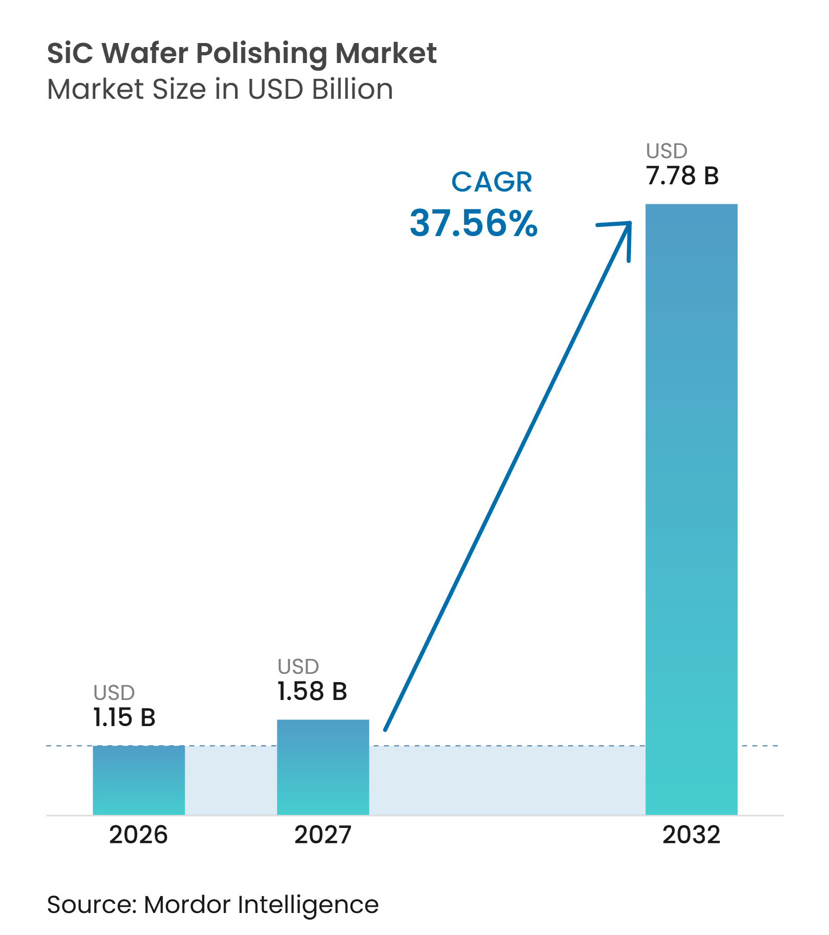
The SiC wafer polishing market size was valued at USD 1.15 billion in 2026 and is estimated to grow from USD 1.58 billion in 2027 to USD 7.78 billion by 2032, at a CAGR of 37.56% during the forecast period (2027-2032). The SiC wafer polishing market is being shaped by the shift from conventional silicon to wide-bandgap materials in power electronics. Silicon carbide has a Mohs hardness of 9, which means its surface preparation requires dedicated pads, slurries, and equipment rather than standard silicon polishing supplies. Automotive electrification and renewable power conversion are increasing wafer demand while also raising surface-quality requirements. The transition from 150 mm to 200 mm substrates is driving demand for larger-format polishing tools and consumables. Suppliers with qualified slurry chemistry, pad formulations, and process knowledge are positioned to benefit as fabs increase output.
Key Report Takeaways
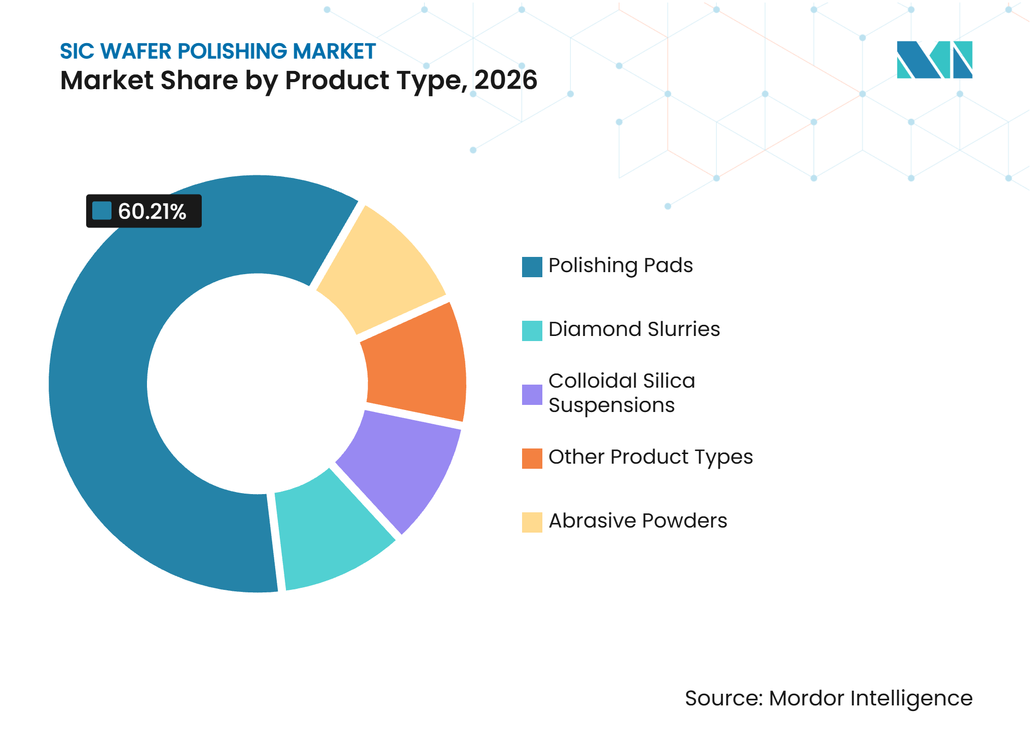
- By product type, polishing pads held 60.21% of the market share in 2026 and are forecast to grow at a 38.93% CAGR through 2032.
- By process type, chemical-mechanical polishing accounted for 55.17% of market share in 2026 and is forecast to grow at a 40.17% CAGR through 2032.
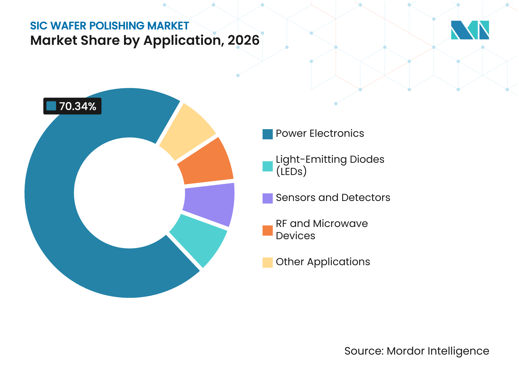
- By application, power electronics accounted for 70.34% of market share in 2026 and is projected to expand at a 42.61% CAGR through 2032.
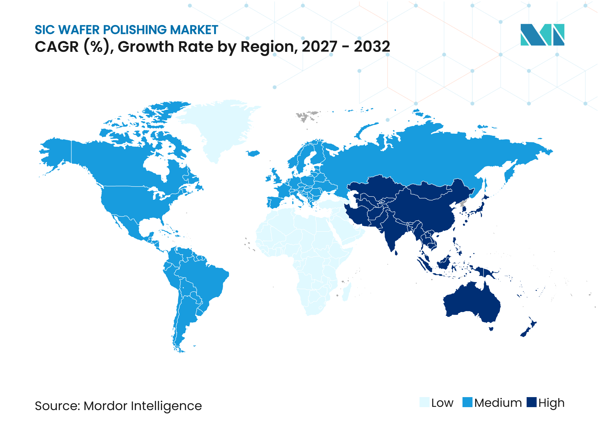
- By geography, Asia-Pacific held 40.38% market share in 2026 and is forecast to grow at a 40.04% CAGR through 2032.
Note: Market numbers in this report are based on Mordor Intelligence's proprietary estimation framework, which combines nine months of actuals with Q4 projections for base year 2026.
Market Trends and Insights
Drivers Impact Analysis of SiC Wafer Polishing Market*
| Drivers | (~) % Impact on CAGR Forecast | Geographic Relevance | Impact Timeline |
|---|---|---|---|
| EV Inverter and Onboard-Charger Deployment | +14.5% | Global, concentrated in China, Europe, and North America | Short term (≤ 2 years) |
| Renewable-Energy Power-Conversion Demand | +8.5% | Global, with APAC and Europe leading in utility-scale solar and North America adding data center Uninterruptible Power Supply (UPS) demand | Medium term (2-4 years) |
| Transition from 6-Inch to 8-Inch SiC Wafers | +7.0% | Global, with early volume in Japan, South Korea, and the United States and ramp-up in China | Medium term (2-4 years) |
| Advanced Chemical Mechanical Planarization (CMP) Consumables and Surface-Quality Requirements | +5.0% | Global, with the highest relevance in APAC fab clusters and European device manufacturing | Long term (≥ 4 years) |
| AI-Enabled In-Line Metrology and Closed-Loop Polishing | +4.0% | Global, with North America and Japan leading patent activity | Long term (≥ 4 years) |
| Source: Mordor Intelligence | |||
EV Inverter and Onboard-Charger Deployment
The SiC wafer polishing market benefits as SiC Metal-Oxide-Semiconductor Field-Effect Transistors (MOSFETs) become a preferred design choice for EV traction inverters using 800-volt battery systems. Their use is also extending to onboard chargers, where faster switching can support compact charging stages rated from 7 kW to 22 kW. ROHM introduced compact HSDIP20 SiC modules for onboard charger power factor correction in April 2025, reporting more than 3 times the power density of top-cooled discrete designs. BYD disclosed a 1,000 kW peak-charging platform in March 2025 that uses high-voltage SiC power chips. Tighter device geometry leaves less tolerance for subsurface damage, increasing the need for longer, more chemically active CMP steps. Onsemi reported resilient demand for SiC from Chinese and European EV customers in May 2025, despite uncertainty over US tariffs.
Renewable-Energy Power-Conversion Demand
The SiC wafer polishing market also benefits from renewable energy systems that require efficient power conversion. Large solar inverters are adopting SiC devices because they can achieve system efficiency above 99%, compared with 98% to 98.5% for silicon Insulated Gate Bipolar Transistor (IGBT) designs. Full-power wind converters also benefit from lower thermal stress, particularly in offshore installations where maintenance costs are high. A 2025 review identified wide-bandgap semiconductors as important for integrating large shares of renewable energy into electricity systems and reducing conversion losses. Grid equipment often operates continuously at high voltage, so manufacturers require very low defect densities and high-purity final polishing. This requirement supports demand for colloidal silica finishing steps and qualified CMP consumables.
Transition from 6-Inch to 8-Inch SiC Wafers
The transition from 150 mm to 200 mm SiC wafers supports the SiC wafer polishing market, as it requires new polishing lines and consumables designed for larger substrates. A 200 mm wafer provides 78% more die area than a 150 mm wafer, thereby reducing device costs and extending the use of SiC beyond premium EV platforms. Wolfspeed generated more revenue from 200 mm substrates than from 150 mm substrates, while Infineon and Bosch entered production in 2025. Onsemi is developing a EUR 1.64 billion SiC facility in the Czech Republic, supported by a EUR 450 million grant under the European Chips Act, with commercial operations planned for 2027. Larger wafers require a total thickness variation of less than 0.3 μm and a surface roughness of less than 0.1 nm Ra for epitaxial-ready production. Japan has also directed support toward SiC wafer capacity through its semiconductor infrastructure program.
Advanced Chemical Mechanical Polishing (CMP) Consumables and Surface-Quality Requirements
The SiC wafer polishing market is moving toward slurry and pad systems that increase material removal rates while limiting surface defects. These objectives can conflict because SiC CMP depends on the balance between chemical oxidation and mechanical abrasion. A 2025 study found that the C-face of 4H-SiC can be polished 3.5 times faster than the Si-face under the same slurry conditions, underscoring the importance of adaptive process control. Entegris developed a recyclable SiC CMP slurry that can return up to 80% of used slurry to production while reducing hazardous waste by more than 75%. Vibrantz introduced its abrasive-free SRS2550 SiC slurry in October 2025 and reported a 0.7-0.8 Å surface finish and up to 99% usable wafer area. China also has active standards projects for 200-mm polished monocrystalline SiC wafers and residual-stress testing.
Restraints Impact Analysis of SiC Wafer Polishing Market*
| Restraints | (~) % Impact on CAGR Forecast | Geographic Relevance | Impact Timeline |
|---|---|---|---|
| Extreme Hardness, Brittleness, and Defectivity | -0.8% | Global, most acute for fabs scaling to 8-inch wafers without established process recipes | Short term (≤ 2 years) |
| Long Cycle Times and Low Material-Removal Rates | -0.5% | Global, with a stronger effect on high-volume automotive-grade production lines | Medium term (2-4 years) |
| Proprietary Recipes and Limited Process Interoperability | -0.3% | Global, most constraining where fewer qualified consumable suppliers are available | Long term (≥ 4 years) |
| Source: Mordor Intelligence | |||
Extreme Hardness, Brittleness, and Defectivity
The SiC wafer polishing market faces process constraints due to SiC's Mohs hardness of 9 and brittleness. Even optimized CMP slurries achieve material removal rates of only 4-7 µm/hour on the Si face. Surface defects can become dislocations in the epitaxial layer, reducing breakdown voltage and switching reliability in finished devices. This issue is more pronounced for 200 mm wafers, which carry a higher risk of edge roll and thickness variation than 150 mm wafers. A 2025 study found that ultrasonic chemical-corrosion approaches still require careful calibration to avoid creating new subsurface damage. These yield constraints limit the rate at which new polishing capacity converts into usable wafer supply.
Long Cycle Times and Low Material-Removal Rates
The SiC wafer polishing market is constrained by preparation cycles that are significantly longer than comparable silicon processes. Coarse grinding, fine grinding, mechanical polishing, and CMP can each require several hours per batch. Longer cycles raise capital requirements and increase the risk of breakage during large-diameter processing. Engis reported that its HYPREZ Grind-to-CMP system reduced CMP planarization time by 66% for 150 mm to 165 mm wafers[1]. However, fabs still need to requalify the full process before adoption. These throughput limitations can reduce the expected cost advantage of 200 mm wafers in applications that are more sensitive to device cost.
*Our forecasts treat driver/restraint impacts as directional, not additive. The impact forecasts reflect baseline growth, mix effects, and variable interactions.
SiC Wafer Polishing Market Segment Analysis
By Product Type:
Polishing Pads Lead Revenue and GrowthPolishing pads held 60.21% of the SiC wafer polishing market share in 2026 and are forecast to grow at a 38.93% CAGR through 2032. This reflects higher CMP step counts and rising pad consumption as wafer geometry requirements become more stringent. Pads play a central role in CMP because their pore structure, groove pattern, and hardness influence surface condition alongside slurry chemistry. The SiC wafer polishing market favors pad suppliers that can deliver stable performance across a range of wafer sizes. Fujibo Holdings held an estimated 80% global share of CMP soft pads, a category used in final SiC polishing.
Fujibo announced an investment of JPY 8.7 billion (~USD 0.05 billion) at its Mibu-gawa factory in November 2025 to raise CMP soft-pad production by 60% by late fiscal 2028. The company is also building a JPY 6.5 billion research center in Taiwan, with an operational target in the first half of fiscal 2027, to work with Asian fabs on pad-and-slurry combinations. Abrasive powders remain important for initial grinding and lapping, where larger wafers require substantial material removal. Diamond slurries are used for intermediate mechanical polishing, while colloidal silica suspensions are used for final finishing. Colloidal silica is gaining relevance as surface roughness requirements move below 0.1 nm Ra.



By Process Type:
CMP Defines Surface-Quality PerformanceChemical-mechanical polishing held 55.17% of revenue in 2026 and is forecast to grow at a 40.17% CAGR through 2032. CMP combines chemical oxidation with abrasive removal and is the established route to sub-nanometer roughness without creating fresh subsurface damage. This capability is important for both Si and C faces of SiC substrates. The SiC wafer polishing market size for CMP benefits from requirements for epitaxial-ready surfaces in automotive, industrial, and energy devices. Semiconductor Equipment and Materials International (SEMI) identified gaps in real-time CMP metrology in its August 2025 auxiliary report.
Mechanical polishing remains important for removing surface damage from sawing and grinding. Pureon AG introduced processes that combine IRINO-PROSiC composite pads and diamond suspensions to achieve a total thickness variation of below 1 µm on 150 mm SiC wafers without intermediate pad conditioning. Electropolishing and plasma-assisted polishing remain smaller methods used mainly for research applications or specific polytypes. Recent work on UV-cured pads and catalytic composite abrasives reflects continuing interest in stress-free finishing approaches. Chemical polishing is also advancing as fabs test abrasive-free final-polishing methods intended to reduce scratch defects.
By Application:
Power Electronics Holds the Largest PositionPower electronics accounted for 70.34% of revenue in 2026 and is projected to grow at a 42.61% CAGR through 2032. EV inverters, onboard chargers, industrial motor drives, and renewable-energy converters are shifting from silicon toward SiC devices. Automotive qualification requirements are particularly demanding because wafer makers must meet specific surface and defect standards. This gives qualified consumable suppliers a more durable position in the supply chain. The SiC wafer polishing market is also benefiting from demand for data-center uninterruptible power supplies that use high-efficiency SiC power devices.
LED applications retain a material but declining role because gallium nitride (GaN)-on-silicon is reducing the use of SiC substrates in LED production. This shift raises the average surface-quality requirement, as power-device substrates need tighter finishing specifications. Sensors, detectors, and RF devices remain smaller applications with distinct material needs. RF devices use semi-insulating SiC substrates and may require CMP chemistries that differ from those used for conductive power-device substrates.

Geography Analysis
Asia-Pacific
Asia-Pacific held 40.38% of the SiC wafer polishing market share in 2026 and is forecast to grow at a 40.04% CAGR through 2032. China supports regional demand through investment in SiC manufacturing, large-scale EV deployment, and renewable energy expansion. The YOFC SiC wafer facility in Wuhan began production in 2025 with an annual capacity of 360,000 wafers, sufficient to supply chips for 1.44 million new-energy vehicles[2]. China's 2025 tax policy notice includes polishing pads and slurries among the materials eligible for preferential treatment. Japan contributes through Fujibo, Fujimi, and JSR, while South Korea and Taiwan are working to qualify 200 mm SiC processes and strengthen co-development opportunities for materials suppliers.
North America
North America is a major market for SiC wafer polishing, encompassing wafer suppliers, device makers, and consumable developers. Wolfspeed's shift toward 200 mm substrate revenue supports recurring demand for qualified CMP products, while Entegris supplies Epic Power CMP pads and slurry-recycling systems for high-capacity fabs. US chip incentives support new wafer capacity requiring larger-format polishing tools and consumables, while Engis offers Grind-to-CMP solutions for 150 mm and 200 mm wafers. Compliance factors include OSHA requirements and EPA semiconductor air-emissions rules for slurry handling and waste treatment. EPA and OSHA renewed cooperation on chemical safety in January 2025, reinforcing chemical management standards across manufacturing sites.
Europe, Southeast Asia, and Emerging Regions
Europe is expanding its role in SiC power-device production through Onsemi's planned integrated facility in the Czech Republic. The facility is expected to begin commercial operations in 2027 and will cover stages from crystal growth to finished devices. Infineon is transitioning its Kulim, Malaysia site from 150 mm to 200 mm wafer production, creating demand in Southeast Asia. The European Union's Critical Raw Materials Act supports upstream supply chains, while Brazil, Saudi Arabia, and India are increasing their focus on SiC power electronics through initiatives in renewable energy and semiconductors.
Competitive Landscape
Market Concentration
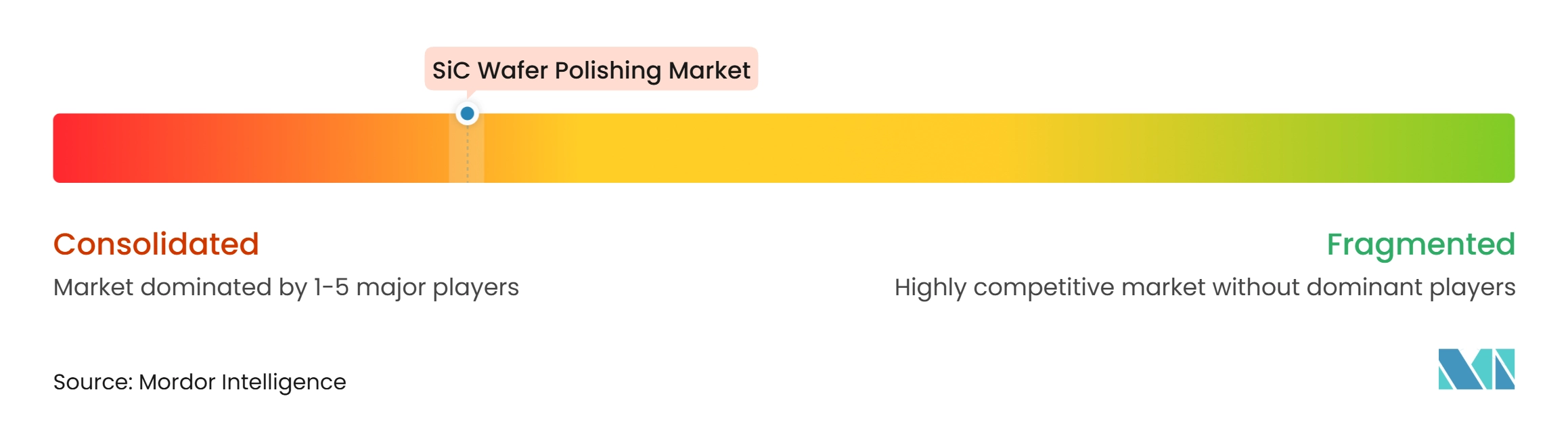
The SiC wafer polishing market is consolidated. Entegris and Fujimi are established suppliers for SiC substrate planarization, while Fujibo holds a strong position in soft CMP pads. Qnity Electronics, formerly DuPont's Electronics business, addresses hard CMP pad requirements through its Ikonic and Emblem product families. Fab qualification cycles make it difficult to replace approved materials. Fujibo's estimated 80% global soft-pad market share reflects the concentration in final-polishing consumables.
In October 2025, Qnity signed a long-term CMP pad supply memorandum with SK Hynix for next-generation semiconductor manufacturing. The agreement illustrates how suppliers use multiyear arrangements to secure demand rather than relying on spot sales. Vibrantz Technologies presented its abrasive-free SRS2550 slurry at 2025 semiconductor events, highlighting chemical removal methods that may reduce particle-related defects. This approach could challenge established slurry suppliers if it achieves full production qualification. Competition is also shifting toward products designed specifically for 200 mm wafers.
Process intelligence represents an additional area of competition in the SiC wafer polishing market. A U.S. patent issued in March 2025 covers machine-vision input for CMP process-control algorithms. SEMI's CMP metrology report indicates that in-situ measurement remains underdeveloped across the market. Equipment and consumable suppliers that can combine materials with monitoring tools may gain a competitive advantage. Proprietary recipes and limited interoperability continue to act as barriers for both buyers and suppliers. The market therefore combines high technical barriers with opportunities in 200 mm formulations and closed-loop polishing control.
SiC Wafer Polishing Industry Leaders
-
DuPont
-
Entegris
-
FUJIBO HOLDINGS, INC.
-
Saint-Gobain
-
Fujimi Incorporated
- *Disclaimer: Major Players sorted in no particular order
SiC Wafer Polishing Market Companies Covered in this Report
- 3M
- DuPont
- Engis Corporation
- Entegris
- FUJIBO HOLDINGS, INC.
- Fujimi Incorporated
- ILJIN DIAMOND CO., LTD.
- JSR Corporation
- Kemet International Limited
- Lapmaster Wolters
- Logitech Ltd.
- Pureon AG
- Saint-Gobain
- SKC
- Vibrantz
Recent Industry Developments in SiC Wafer Polishing Market
- January 2026: Fujibo Holdings announced a JPY 8.7 billion capacity expansion investment at the Fujibow Ehime Mibu-gawa factory to increase CMP soft pad production by over 60%, targeting semiconductor CMP applications driven by AI-related demand, with operations expected from the second half of fiscal year 2028. The company is also constructing a JPY 6.5 billion research and development center in Taiwan, expected to be operational by the first half of fiscal year 2027, to co-develop SiC Wafer Polishing-compatible pad architectures with Asian foundries.
- November 2025: The European Commission approved a EUR 450 million (~USD 501.99 million) Czech Republic state aid grant to Onsemi for establishing an integrated SiC power device manufacturing facility in Rožnov pod Radhoštěm, covering all processes from crystal growth to finished devices. The facility is expected to begin commercial operations by 2027 and will be the first fully integrated SiC Wafer Polishing production site in the EU, representing a direct expansion of demand for polishing consumables in Europe.
Global SiC Wafer Polishing Market Report Scope
SiC wafer polishing is a precision finishing process used to make a silicon carbide (SiC) single-crystal substrate mirror-flat, atomically smooth, and free of subsurface damage before it is used to manufacture high-power or high-frequency electronic devices.
The SiC wafer polishing market is segmented by product type, process type, application, and geography. By product type, the market is segmented into abrasive powders, polishing pads, diamond slurries, colloidal silica suspensions, and other product types. By process type, the market is segmented into mechanical polishing, chemical-mechanical polishing (CMP), electropolishing, chemical polishing, plasma-assisted polishing, and other process types. By application, the market is segmented into power electronics, light-emitting diodes (LEDs), sensors and detectors, RF and microwave devices, and other applications. The report also covers market sizes and forecasts for SiC wafer polishing across 15 countries in major regions. The market sizes and forecasts are provided in terms of value (USD).
Segmentation Overview
| Abrasive Powders |
| Polishing Pads |
| Diamond Slurries |
| Colloidal Silica Suspensions |
| Other Product Types |
| Mechanical Polishing |
| Chemical-Mechanical Polishing (CMP) |
| Electropolishing |
| Chemical Polishing |
| Plasma-Assisted Polishing |
| Other Process Types |
| Power Electronics |
| Light-Emitting Diodes (LEDs) |
| Sensors and Detectors |
| RF and Microwave Devices |
| Other Applications |
| Asia-Pacific | China |
| India | |
| Japan | |
| South Korea | |
| Rest of Asia-Pacific | |
| North America | United States |
| Canada | |
| Mexico | |
| Europe | Germany |
| United Kingdom | |
| France | |
| Italy | |
| Rest of Europe | |
| South America | Brazil |
| Argentina | |
| Rest of South America | |
| Middle East and Africa | Saudi Arabia |
| South Africa | |
| Rest of Middle East and Africa |
| By Product Type | Abrasive Powders | |
| Polishing Pads | ||
| Diamond Slurries | ||
| Colloidal Silica Suspensions | ||
| Other Product Types | ||
| By Process Type | Mechanical Polishing | |
| Chemical-Mechanical Polishing (CMP) | ||
| Electropolishing | ||
| Chemical Polishing | ||
| Plasma-Assisted Polishing | ||
| Other Process Types | ||
| By Application | Power Electronics | |
| Light-Emitting Diodes (LEDs) | ||
| Sensors and Detectors | ||
| RF and Microwave Devices | ||
| Other Applications | ||
| By Geography | Asia-Pacific | China |
| India | ||
| Japan | ||
| South Korea | ||
| Rest of Asia-Pacific | ||
| North America | United States | |
| Canada | ||
| Mexico | ||
| Europe | Germany | |
| United Kingdom | ||
| France | ||
| Italy | ||
| Rest of Europe | ||
| South America | Brazil | |
| Argentina | ||
| Rest of South America | ||
| Middle East and Africa | Saudi Arabia | |
| South Africa | ||
| Rest of Middle East and Africa | ||
Key Questions Answered in the Report
What is current market size of SiC Wafer Polishing Market?
The SiC wafer polishing market size was valued at USD 1.15 billion in 2026 and is estimated to grow from USD 1.58 billion in 2027 to USD 7.78 billion by 2032, at a CAGR of 37.56% during the forecast period (2027-2032).
Which SiC wafer polishing product has the largest share?
Polishing pads lead with a 60.21% share in 2026 and are expected to grow at a 38.93% CAGR through 2032.
Which application accounts for the largest SiC wafer polishing demand?
Power electronics account for a 70.34% share in 2026 and are forecast to expand at a 42.61% CAGR through 2032.
Which region leads SiC wafer polishing demand?
Asia-Pacific leads with a 40.38% share in 2026 and is projected to grow at a 40.04% CAGR through 2032.