High Bandwidth Memory Market Size and Share
Market Overview
| Study Period | 2020 - 2031 |
|---|---|
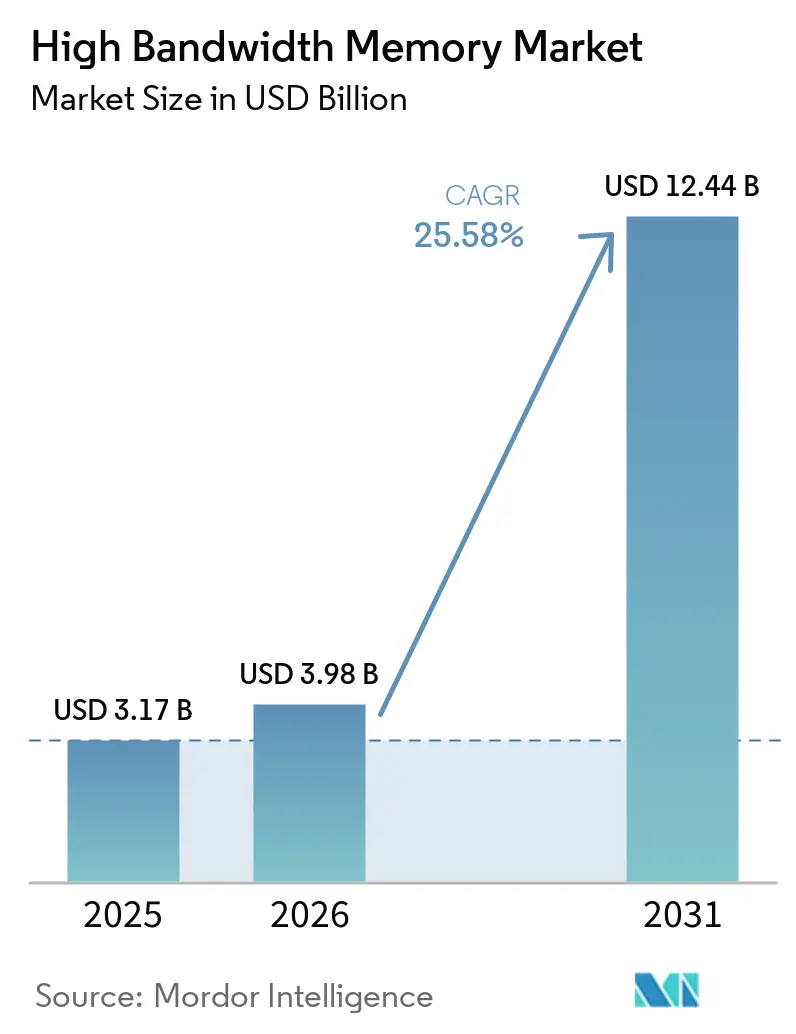
| Market Size (2026) | USD 3.98 Billion |
| Market Size (2031) | USD 12.44 Billion |
| Growth Rate (2026 - 2031) | 25.58% CAGR |
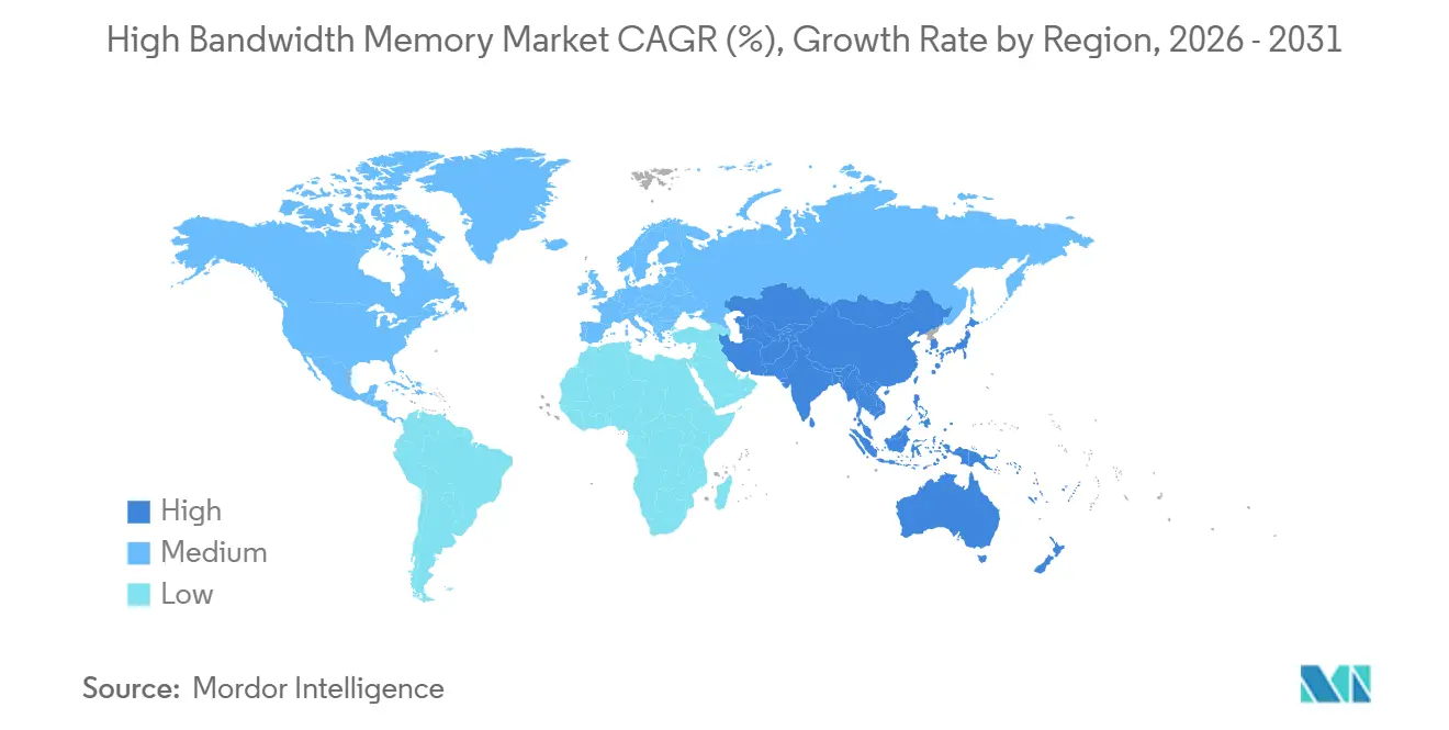
| Fastest Growing Market | Asia Pacific |
| Largest Market | Asia Pacific |
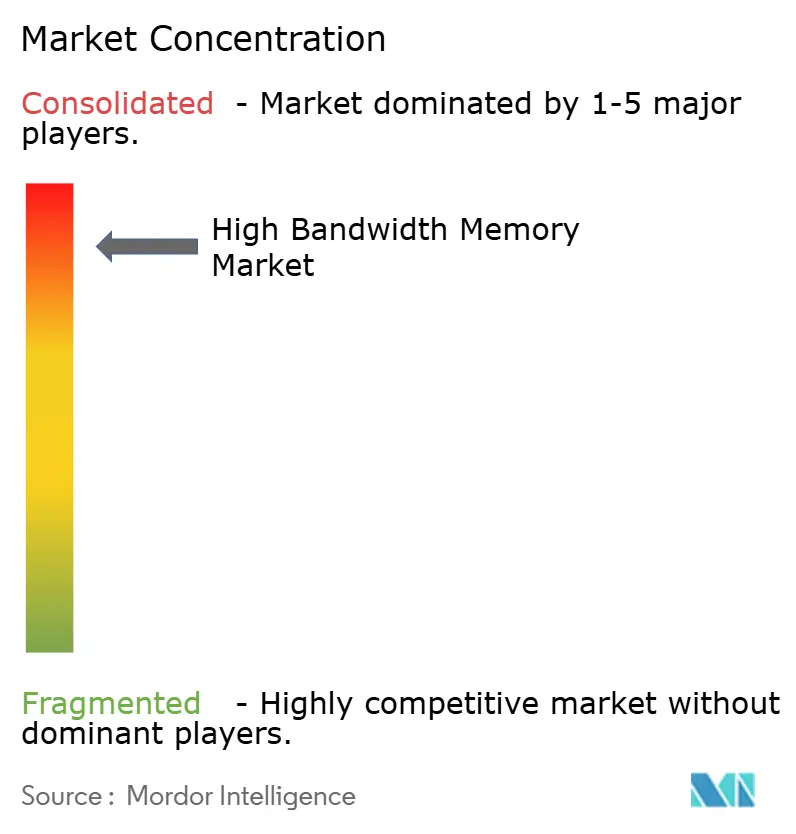
| Market Concentration | High |
Major Players *Disclaimer: Major Players sorted in no particular order Image © Mordor Intelligence. Reuse requires attribution under CC BY 4.0. | |
High Bandwidth Memory Market Analysis by Mordor Intelligence
The High Bandwidth Memory market size is expected to increase from USD 3.17 billion in 2025 to USD 3.98 billion in 2026 and reach USD 12.44 billion by 2031, growing at a CAGR of 25.58% over 2026-2031. Sky-high bandwidth requirements in generative-AI clusters are pushing hyperscalers to abandon conventional GDDR and DDR in favor of vertically stacked DRAM that delivers more than 2.8 terabytes per second of bandwidth per stack. Server-class deployments still dominate shipments, yet edge inference in vehicles and industrial gateways is accelerating adoption outside traditional data centers. Advanced 2.5-D packaging capacity has emerged as a bottleneck, giving memory suppliers unprecedented pricing power and aligning their roadmaps tightly with foundry partners’ interposer innovations. Government subsidies topping USD 100 billion across Asia-Pacific and North America are underwriting rapid fab expansions, while export-control regimes are bifurcating supply chains and driving regionalization. Collectively, these forces indicate that bandwidth, not raw compute, is the new performance ceiling in AI infrastructure, and that the High Bandwidth Memory market will remain structurally supply-constrained through the end of the decade.
Key Report Takeaways
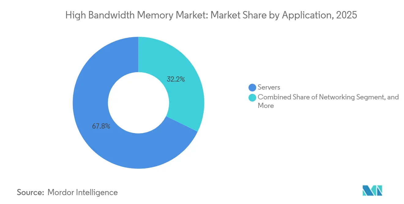
- By application, servers led with 67.80% revenue share in 2025, while automotive and transportation are projected to grow at a 26.58% CAGR through 2031.
- By technology, HBM3 captured 45.70% of 2025 revenue, whereas HBM3E is forecast to expand at 26.43% over 2026-2031.
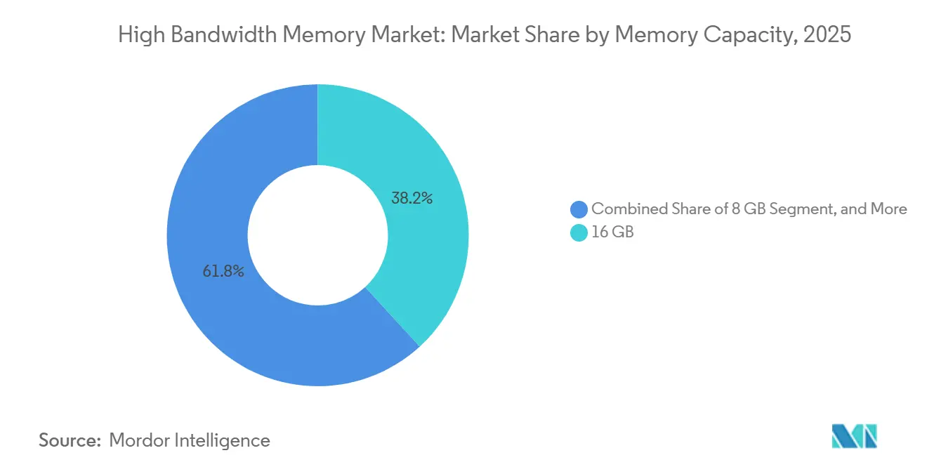
- By memory capacity per stack, the 16-gigabyte tier accounted for 38.20% of 2025 shipments, but 32-gigabyte and above configurations are advancing at a 26.56% CAGR to 2031.
- By processor interface, GPUs held 63.60% revenue share in 2025, while AI accelerators and ASICs are set to grow at 25.62% through 2031.
- By geography, Asia-Pacific commanded a 41.00% share in 2025 and is on track for a 26.66% CAGR during 2026-2031.
Note: Market size and forecast figures in this report are generated using Mordor Intelligence’s proprietary estimation framework, updated with the latest available data and insights as of 2026.
Global High Bandwidth Memory Market Trends and Insights
Drivers Impact Analysis*
| Driver | (~) % Impact on CAGR Forecast | Geographic Relevance | Impact Timeline |
|---|---|---|---|
| AI-Server Proliferation and GPU Attach Rates | +8.2% | Global, concentrated in North America and Asia-Pacific hyperscaler hubs | Short term (≤ 2 years) |
| Data-Center Shift to DDR5 and 2.5-D Packaging | +6.1% | Global, led by North America and Europe enterprise deployments | Medium term (2-4 years) |
| Hyperscaler Preference for Silicon Interposers | +5.4% | North America and Asia-Pacific, with spillover to Europe | Medium term (2-4 years) |
| Localized Memory Production Subsidies | +3.7% | South Korea, Japan, United States | Long term (≥ 4 years) |
| Edge-AI Inference in Automotive ADAS | +1.6% | Global, early in Europe and North America, scaling in Asia-Pacific | Long term (≥ 4 years) |
| Photonics-Ready HBM Roadmaps (HBM-P) | +0.8% | North America and Asia-Pacific research clusters | Long term (≥ 4 years) |
| Source: Mordor Intelligence | |||


AI-Server Proliferation and GPU Attach Rates
Enterprises are pivoting toward GPU-dense servers that demand four to eight HBM stacks per node to keep pace with transformer models exceeding one trillion parameters. Dell Technologies reported AI-optimized server revenue up 80% year over year in fiscal 2025, illustrating how traditional OEMs are profiting from this pivot. Non-traditional buyers such as Bitcoin miner-turned-AI provider IREN have ordered 20,000 Nvidia H200 GPUs, each with 141 GB of HBM3E, confirming that bandwidth needs spill across verticals. As model sizes grow, the memory-to-compute ratio continues to climb, locking in multiyear visibility for HBM suppliers. The generational jump from HBM2E to HBM3E raised per-stack bandwidth by 50%, yet developers are already specifying HBM4 for 2027 hardware, compressing product lifecycles and forcing overlapping R&D. Consequently, DRAM makers are capturing a larger share of system bill-of-materials than GPU vendors ever anticipated.
Data-Center Shift to DDR5 and 2.5-D Packaging
Migration from DDR4 to DDR5 has familiarized substrate manufacturers and assembly houses with multi-gigahertz signaling, lowering perceived risk around HBM qualification. By late 2025, DDR5 modules represented over half of server DRAM shipments, and the learning curve in thermal design for 6.4 GT/s interfaces directly benefits HBM packaging. TSMC’s Chip-on-Wafer-on-Substrate process routes thousands of micro-bumps between logic and memory dies, a technology that evolved from earlier 2.5-D field-programmable gate arrays.[1]TSMC, “2.5-D and 3-D Packaging Technologies,” tsmc.com As manufacturing maturity rises, HBM cost premiums have narrowed from 10× to roughly 4× versus commodity DRAM, widening adoption beyond hyperscale AI into high-performance computing and premium graphics cards. Standards bodies have codified interoperability, preventing vendor lock-in and accelerating the diffusion of High Bandwidth Memory across multiple compute domains.
Hyperscaler Preference for Silicon Interposers
Cloud service providers are standardizing on silicon interposers to share vast HBM pools across multi-chip modules. NVIDIA alone locked in 60-65% of TSMC’s advanced-packaging capacity for 2026, leaving limited headroom for rivals. Alternative houses such as ASE Technology doubled advanced-packaging revenue to USD 1.6 billion in 2025 by qualifying fan-out chip-on-substrate and silicon-bridge techniques. Yet TSMC’s installed base and proven yield keep it the gatekeeper for leading AI accelerators. Silicon interposer lead times have stretched beyond 12 months, creating a strategic moat for hyperscalers who pre-book capacity years in advance. Memory vendors have responded by signing joint development agreements; SK hynix and TSMC aligned on HBM4 mass production in 2024, to guarantee the tight coupling of die-stack and interposer roadmaps.
Localized Memory Production Subsidies
South Korea, Japan, and the United States have together pledged more than USD 100 billion in incentives to trim capital intensity for new HBM fabs by up to 40%. Japan’s JPY 10 trillion (USD 65 billion) semiconductor program funded Micron’s USD 9.6 billion expansion in Hiroshima. South Korea’s 33 trillion won (USD 23 billion) package supports Samsung and SK Hynix's clean-room build-outs. The U.S. CHIPS Act awarded USD 6.6 billion to TSMC Arizona and separate grants to Samsung, Intel, and Micron, reinforcing domestic memory sovereignty. Subsidies lower the barrier-to-entry for advanced nodes, but they also split global supply chains into regulated and unregulated zones, creating regional price differentials that will persist throughout the forecast.
Restraints Impact Analysis*
| Restraint | (~) % Impact on CAGR Forecast | Geographic Relevance | Impact Timeline |
|---|---|---|---|
| Limited CoWoS/SoIC advanced-packaging capacity | -4.3% | Global, acute in Taiwan | Short term (≤ 2 years) |
| Geo-political export controls on AI accelerators | -2.8% | China demand suppression, spillover to Middle East and Africa | Medium term (2-4 years) |
| TSV yield losses above 12-layer stacks | -1.9% | Global, affecting all HBM4 ramps | Medium term (2-4 years) |
| Thermal throttling in >1 TB/s devices | -1.2% | Global, concentrated in AI training clusters | Long term (≥ 4 years) |
| Source: Mordor Intelligence | |||
Limited CoWoS/SoIC Advanced-Packaging Capacity
TSMC’s CoWoS and SoIC lines reached roughly 120,000 wafers per month by late 2025, but Nvidia alone reserved more than half of that volume for 2026. Short-run alternatives at ASE, Amkor, and JCET offer fan-out or silicon-bridge options, yet these processes lag in yield and customer qualifications, forcing second-tier chip designers to accept longer validation cycles or reduced performance. Although TSMC earmarked part of its USD 44-50 billion in fiscal 2026 capex for new packaging capacity in Arizona, near-term supply remains inelastic. Consequently, packaging capacity, not wafer starts, is the gating factor for High Bandwidth Memory market growth through 2028, and customers with multi-source strategies command premium allocations.
Geo-Political Export Controls on AI Accelerators
The U.S. Bureau of Industry and Security re-classified HBM with a DRAM half-pitch of 18 nm or below as an advanced computing item in December 2024, imposing license requirements that cap shipments to China-based projects.[2]Bureau of Industry and Security, “License Exception HBM,” bis.doc.gov Samsung and SK hynix historically derived up to 30% of HBM revenue from China, forcing them to redirect product toward allied markets or accept idle capacity in legacy HBM2E lines. Chinese fabs, including ChangXin Memory Technologies, aim to deliver domestic HBM3 by 2026, yet ecosystem and yield hurdles push commercial parity beyond the forecast window. The result is a bifurcated market structure with premium pricing for export-compliant nodes and margin compression on unrestricted legacy parts.
*Our forecasts treat driver/restraint impacts as directional, not additive. The impact forecasts reflect baseline growth, mix effects, and variable interactions.
Segment Analysis
By Application: Servers Drive Volume As Automotive Accelerates
Servers accounted for 67.80% of the total 2025 revenue, making them the anchor of the High Bandwidth Memory market size at USD 3.17 billion. Hyperscale data centers deploy four to eight HBM stacks per GPU, translating to hundreds of petabytes of addressable demand annually. Networking equipment, such as 800-Gb Ethernet line cards, uses HBM to meet ultra-low-latency thresholds but accounts for only a modest slice of revenue. High-performance computing centers are transitioning from HBM2E to HBM3E to reduce time-to-solution on memory-bound algorithms.
Automotive platforms represent the fastest-growing slice, advancing at a 26.58% CAGR as centralized compute domains consolidate sensor fusion and path planning on single SoCs that integrate HBM. NVIDIA’s Drive Thor delivers 2,000 TOPS with on-package HBM to digest nearly 1 TB of sensor data per hour. Premium consumer graphics cards still leverage stacked DRAM, but cost-sensitive SKUs favor GDDR because gaming workloads are less bandwidth-constrained. The strategic implication is that design-win longevity in automotive, combined with stringent safety certifications, creates thicker margins than hyperscale refresh cycles can offer.


By Technology: HBM3E Surges While HBM4 Samples Ramp
HBM3 accounted for 45.70% of the revenue in 2025, driven by its widespread adoption across high-performance computing and AI applications. However, HBM3E is anticipated to drive growth at 26.43%, as suppliers increasingly qualify 12-layer stacks capable of exceeding 3 TB/s. These advanced stacks offer significantly higher bandwidth, which reduces the number of packages required per accelerator. This, in turn, minimizes interposer area and enhances overall yield. Meanwhile, HBM2 and HBM2E are experiencing a steady decline, with their usage now largely confined to networking and legacy compute systems.
Sampling of HBM4 commenced in early 2025, marking a significant milestone in memory technology. SK Hynix was the first to ship 12-layer modules, with Samsung following closely behind a few months later. The specifications for HBM4 are impressive, featuring more than 10 Gb/s per pin and stack bandwidth exceeding 2 TB/s. Additionally, HBM4 offers a 40% improvement in energy efficiency compared to HBM3E, making it a highly attractive option for next-generation applications. The transition to volume production is expected to begin in 2026, likely accelerating the shift in revenue share toward HBM4 by the end of the decade. This evolution is also expected to pave the way for photonics-ready HBM variants, projected to emerge between 2028 and 2029.
By Memory Capacity Per Stack: Larger Stacks Gain Ground
The 16 GB tier held 38.20% market share in 2025, reflecting mainstream AI accelerator configurations. This dominance highlights its suitability for a wide range of applications, particularly in AI and machine learning workloads. However, 32 GB and above stacks are projected to grow at a compound annual growth rate (CAGR) of 26.56% through 2031. This growth is driven by hyperscaler roadmaps that aim to increase per-GPU capacity to 384 GB, addressing the rising demand for higher computational power and memory bandwidth in advanced AI systems. For instance, AMD’s MI325X already integrates 288 GB of HBM3E, showcasing the industry's shift toward higher memory capacities. Additionally, both SK hynix and Samsung are actively validating 48 GB, 16-layer HBM4 configurations, which are expected to be ready for deployment in 2026 clusters.
Reducing the number of packages per board significantly reduces interposer routing complexity, thereby lowering the total cost of ownership for end users. This trend underscores the importance of capacity per stack rather than just raw capacity per system, as it has become a critical factor in determining the overall bill of materials. Suppliers with established, proven 16-layer manufacturing processes are well positioned to capture a larger market share, as they can meet the growing demand for high-capacity, efficient memory solutions in next-generation computing systems.
By Processor Interface: AI Accelerators Trim GPU Dominance
GPUs accounted for 63.60% of the projected revenue in 2025, maintaining their dominance in the market. However, they are expected to face increasing competition as custom AI accelerators and application-specific integrated circuits (ASICs) grow at a robust rate of 25.62%. This growth is primarily driven by their ability to bypass proprietary ecosystems, offering more tailored and efficient solutions for specific applications. Companies like Marvell and Broadcom have already secured multi-year engagements with hyperscalers for high-bandwidth memory (HBM)-enabled ASICs. Both companies claim to deliver superior compute-to-memory power ratios, which are critical for addressing the growing demand for high-performance computing.
Meanwhile, CPUs with on-package HBM, such as Intel’s Xeon CPU Max, are carving out a niche by addressing memory-bound workloads. These include scientific computing tasks and in-memory databases, where their capabilities are particularly well-suited. Although this segment is smaller compared to GPUs and ASICs, it remains a steady and important part of the market. Field-programmable gate arrays (FPGAs) continue to play a vital role in specific use cases such as low-latency trading and telecom backhaul, where their flexibility and performance are unmatched. Additionally, optical and neuromorphic processors, while still in the pilot phase, are emerging technologies that highlight the future requirements for increased bandwidth. These advancements have the potential to redefine interface hierarchies, paving the way for new innovations in processing and data handling.
Geography Analysis
Asia-Pacific dominated the High Bandwidth Memory market with 41.00% market share in 2025 and is set to grow at a 26.66% CAGR through 2031. The region benefits significantly from government subsidies in countries like South Korea and Japan, which reduce fab costs by 20-40%. These subsidies have enabled companies like SK hynix to achieve an operating margin of 72% on USD 37.1 billion in Q1-2026 revenue. Additionally, Micron’s USD 9.6 billion investment in a new Hiroshima facility aims to diversify non-Chinese supply lines, ensuring a more stable supply chain. Meanwhile, China’s domestic DRAM manufacturers are striving to ramp up HBM3 production volumes by 2026, though they remain 18-24 months behind established players in terms of technological advancements and production capabilities.
North America ranks as the second-largest market, driven by strong hyperscaler demand and significant government support through the CHIPS Act grants. These grants, totaling more than USD 6.6 billion, have been instrumental in developing TSMC’s advanced packaging hub in Arizona.[3]U.S. Department of Commerce, “TSMC Arizona Incentive,” commerce.gov Major U.S.-based companies such as Nvidia, AMD, and Broadcom collectively account for over 70% of global HBM procurement, aligning the region’s supply chain closely with Silicon Valley’s technological roadmaps. Europe, on the other hand, lags due to its limited indigenous DRAM production capacity. However, it remains a critical consumer market, particularly for applications in automotive advanced driver-assistance systems (ADAS) and high-performance computing (HPC) centers.
South America, the Middle East, and Africa collectively represent emerging markets with growing demand, primarily driven by telecommunications infrastructure upgrades and national AI development initiatives. However, these regions face challenges, such as export licensing restrictions and limited local packaging capabilities, which constrain immediate shipment volumes. As a result, these markets are currently viewed as strategic opportunities for future growth rather than primary revenue contributors in the near term.

Competitive Landscape
The High Bandwidth Memory market is highly concentrated, with Samsung, SK hynix, and Micron controlling more than 95% of global output. SK hynix is projected to maintain a dominant market share of over 60% in 2026, driven by its early adoption and successful deployment of HBM3E and HBM4 technologies in Nvidia’s H200 and Blackwell GPUs. Samsung, on the other hand, has been actively working to close the gap, securing a significant agreement in March 2026 to supply HBM4 for AMD’s MI455X platform. Meanwhile, Micron is focusing on scaling up HBM4 production in 2026, with plans to introduce 48 GB stacks capable of delivering 2.8 TB/s, positioning it to compete strongly on capacity and performance.[4]Micron Technology, “HBM4 Product Brief,” micron.com
TSMC’s dominance in Chip-on-Wafer-on-Substrate (CoWoS) capacity further strengthens its upstream leverage, compelling customers to explore dual-sourcing with alternative providers such as ASE, Amkor, and JCET, despite the higher validation costs. Innovation in the market is increasingly centered on photonics-ready HBM and custom memory architectures. For instance, Marvell has developed a custom HBM solution that boasts a 70% reduction in interface power, while Rambus and Cadence have introduced HBM4E controller IP capable of supporting data rates of 16 Gb/s per pin, showcasing advancements in efficiency and performance.
The next major area of competition in the market is expected to revolve around vertical integration, which combines memory, packaging, and interconnect technologies under a unified framework. Hyperscalers that are co-investing in packaging lines are beginning to redefine traditional supplier-customer dynamics. This shift signals the emergence of a new era in the industry, where the ability to manage heat dissipation and yield optimization, rather than merely increasing raw die output, will become the key determinants of market leadership and influence.
High Bandwidth Memory Industry Leaders
Micron Technology, Inc.
Samsung Electronics Co. Ltd.
SK Hynix Inc.
Taiwan Semiconductor Manufacturing Company Limited
ASE Technology Holding Co., Ltd.
- *Disclaimer: Major Players sorted in no particular order

Recent Industry Developments
- April 2026: SK hynix received the IEEE Corporate Innovation Award for breakthroughs in HBM3E and HBM4.
- March 2026: SK hynix received the IEEE Corporate Innovation Award for breakthroughs in HBM3E and HBM4.
- March 2026: Samsung and AMD signed an MoU designating Samsung as the primary HBM4 supplier for MI455X GPUs.
- February 2026: SK Hynix confirmed it will provide HBM4 for Nvidia’s next-generation accelerators.


Global High Bandwidth Memory Market Report Scope
The High Bandwidth Memory (HBM) Market refers to the global industry focused on the development, manufacturing, and commercialization of advanced stacked memory solutions designed to deliver extremely high data bandwidth, low power consumption, and compact form factors for high-performance computing applications. HBM utilizes 3D die stacking and through-silicon vias (TSVs) to enable faster data transfer between memory and processors, making it critical for data-intensive workloads.
The High Bandwidth Memory Report is Segmented by Application (Servers, Networking, High-Performance Computing, Consumer Electronics, and Automotive and Transportation), Technology (HBM2, HBM2E, HBM3, HBM3E, and HBM4), Memory Capacity per Stack (4 GB, 8 GB, 16 GB, 24 GB, and 32 GB and Above), Processor Interface (GPU, CPU, AI Accelerator/ASIC, FPGA, and Other Interfaces), and Geography (North America, South America, Europe, Asia-Pacific, and Middle East and Africa). Market Forecasts are Provided in Terms of Value (USD).
| Servers |
| Networking |
| High-Performance Computing |
| Consumer Electronics |
| Automotive and Transportation |
| HBM2 |
| HBM2E |
| HBM3 |
| HBM3E |
| HBM4 |
| 4 GB |
| 8 GB |
| 16 GB |
| 24 GB |
| 32 GB and Above |
| GPU |
| CPU |
| AI Accelerator / ASIC |
| FPGA |
| Others |
| North America | United States | |
| Canada | ||
| Mexico | ||
| South America | Brazil | |
| Rest of South America | ||
| Europe | Germany | |
| France | ||
| United Kingdom | ||
| Rest of Europe | ||
| Asia-Pacific | China | |
| Japan | ||
| India | ||
| South Korea | ||
| Rest of Asia-Pacific | ||
| Middle East and Africa | Middle East | Saudi Arabia |
| United Arab Emirates | ||
| Turkey | ||
| Rest of Middle East | ||
| Africa | South Africa | |
| Rest of Africa | ||
| By Application | Servers | ||
| Networking | |||
| High-Performance Computing | |||
| Consumer Electronics | |||
| Automotive and Transportation | |||
| By Technology | HBM2 | ||
| HBM2E | |||
| HBM3 | |||
| HBM3E | |||
| HBM4 | |||
| By Memory Capacity per Stack | 4 GB | ||
| 8 GB | |||
| 16 GB | |||
| 24 GB | |||
| 32 GB and Above | |||
| By Processor Interface | GPU | ||
| CPU | |||
| AI Accelerator / ASIC | |||
| FPGA | |||
| Others | |||
| By Geography | North America | United States | |
| Canada | |||
| Mexico | |||
| South America | Brazil | ||
| Rest of South America | |||
| Europe | Germany | ||
| France | |||
| United Kingdom | |||
| Rest of Europe | |||
| Asia-Pacific | China | ||
| Japan | |||
| India | |||
| South Korea | |||
| Rest of Asia-Pacific | |||
| Middle East and Africa | Middle East | Saudi Arabia | |
| United Arab Emirates | |||
| Turkey | |||
| Rest of Middle East | |||
| Africa | South Africa | ||
| Rest of Africa | |||


Key Questions Answered in the Report
What is the current High Bandwidth Memory market size and how fast is it growing?
The High Bandwidth Memory market size stood at USD 3.98 billion in 2026 and is forecast to reach USD 12.44 billion by 2031, reflecting a 25.58% CAGR .
Which end-use segment is expanding the fastest?
Automotive and transportation is projected to post the quickest growth, advancing at a 26.58% CAGR as centralized ADAS compute platforms adopt stacked DRAM for edge inference workloads.
Who are the dominant suppliers of High Bandwidth Memory today?
Samsung, SK hynix, and Micron collectively control more than 95% of global qualified capacity, with SK hynix leading in HBM3E and HBM4 shipments.
How are export controls affecting High Bandwidth Memory supply?
U.S. regulations classify sub-18 nm HBM as an advanced computing item, curbing shipments to certain China-based projects and forcing suppliers to redirect output to allied geographies, which elevates regional pricing.
Why is advanced packaging a bottleneck for High Bandwidth Memory?
TSMC's CoWoS lines are nearly fully booked through 2026, and alternative providers have yet to match its yield, making packaging capacity the gating factor rather than raw wafer output.
What technology generation will lead the market by the end of the decade?
HBM4 is expected to dominate revenue share by 2029 as 12- and 16-layer stacks move into mass production, delivering more than 2 TB/s of bandwidth per package.
Page last updated on:


