CMOS Image Sensors Market Size and Share
Market Overview
| Study Period | 2020 - 2031 |
|---|---|
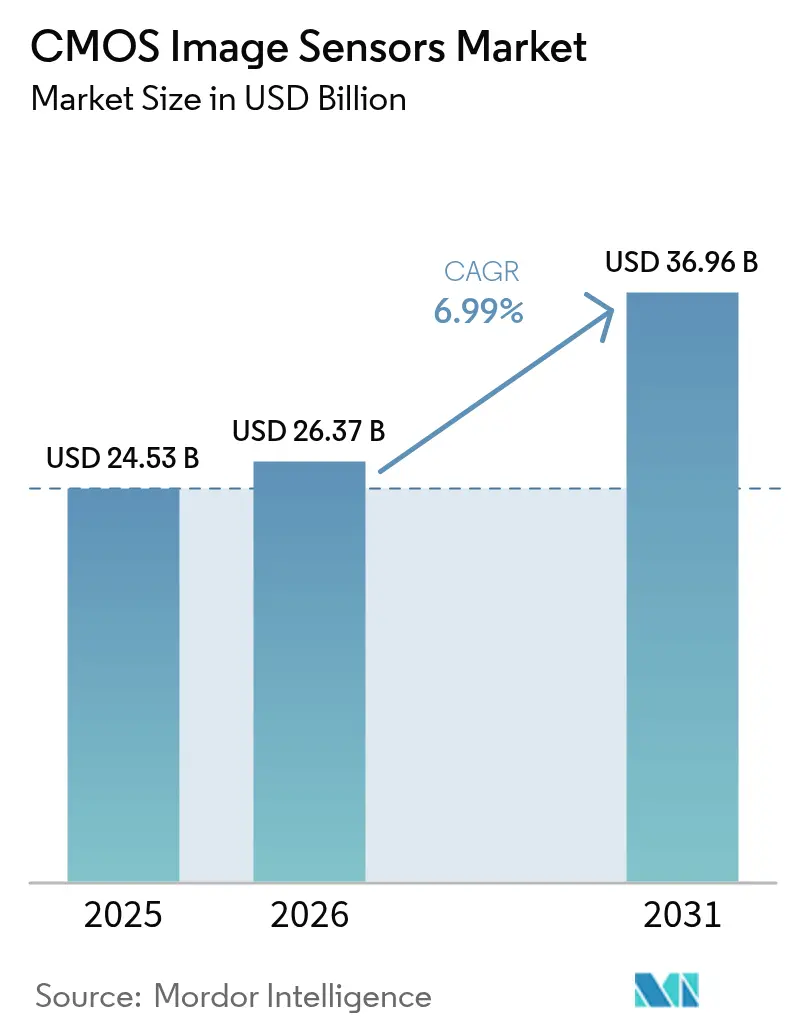
| Market Size (2026) | USD 26.37 Billion |
| Market Size (2031) | USD 36.96 Billion |
| Growth Rate (2026 - 2031) | 6.99% CAGR |
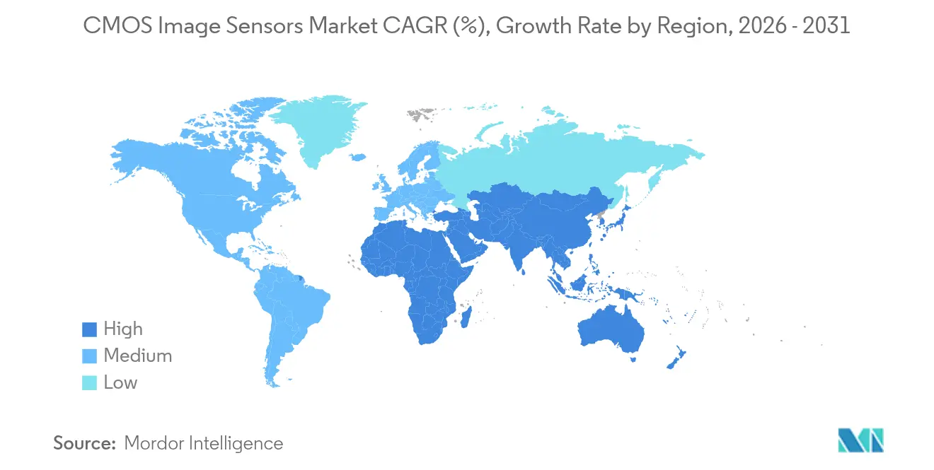
| Fastest Growing Market | Middle East and Africa |
| Largest Market | Asia Pacific |
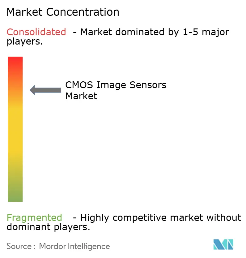
| Market Concentration | High |
Major Players *Disclaimer: Major Players sorted in no particular order Image © Mordor Intelligence. Reuse requires attribution under CC BY 4.0. | |
CMOS Image Sensors Market Analysis by Mordor Intelligence
The CMOS image sensors market size is projected to expand from USD 24.53 billion in 2025 and USD 26.37 billion in 2026 to USD 36.96 billion by 2031, registering a 6.99% CAGR between 2026 and 2031. Premium-tier smartphones integrating four to six cameras, regulatory mandates for automatic emergency braking, and adoption of stacked backside-illuminated designs that embed on-chip intelligence are the principal growth vectors. Module makers shift focus from unit volume toward value-added architectures that separate pixel and logic layers to raise quantum efficiency without increasing die area. Automotive designs now require near-infrared sensitivity at 940 nanometers to meet functional-safety norms, while wireless sensor modules enable untethered surveillance and healthcare devices, trimming installation cost and power budgets.
Key Report Takeaways
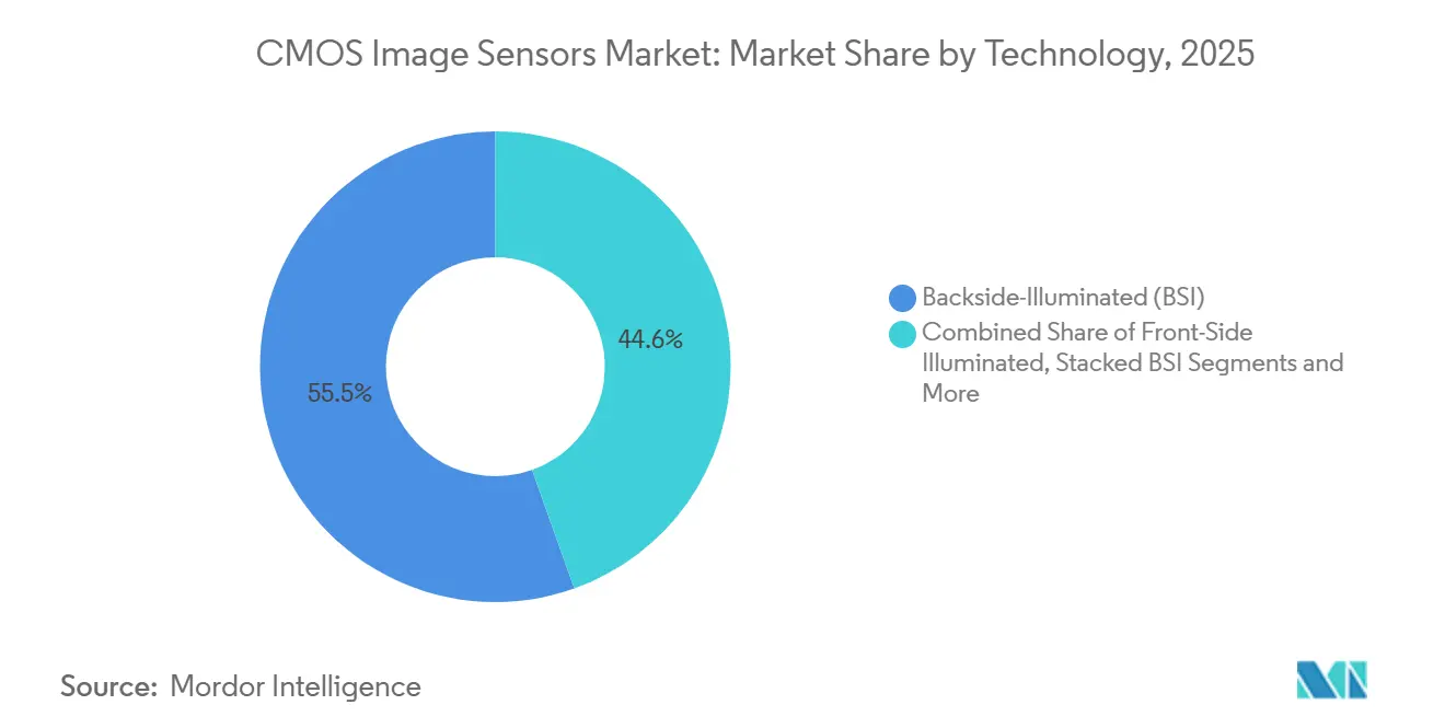
- By technology, backside-illuminated sensors led with 55.45% of the CMOS image sensors market share in 2025, while stacked BSI architectures are forecast to expand at a 7.84% CAGR through 2031.
- By resolution, the 12–24-megapixel band accounted for a 47.29% share of the CMOS image sensors market size in 2025 and sensors greater than 49 megapixels are projected to grow at a 7.25% CAGR to 2031.
- By spectrum, visible-light devices retained 68.14% revenue share in 2025; non-visible variants will advance at a 7.56% CAGR during the forecast window.
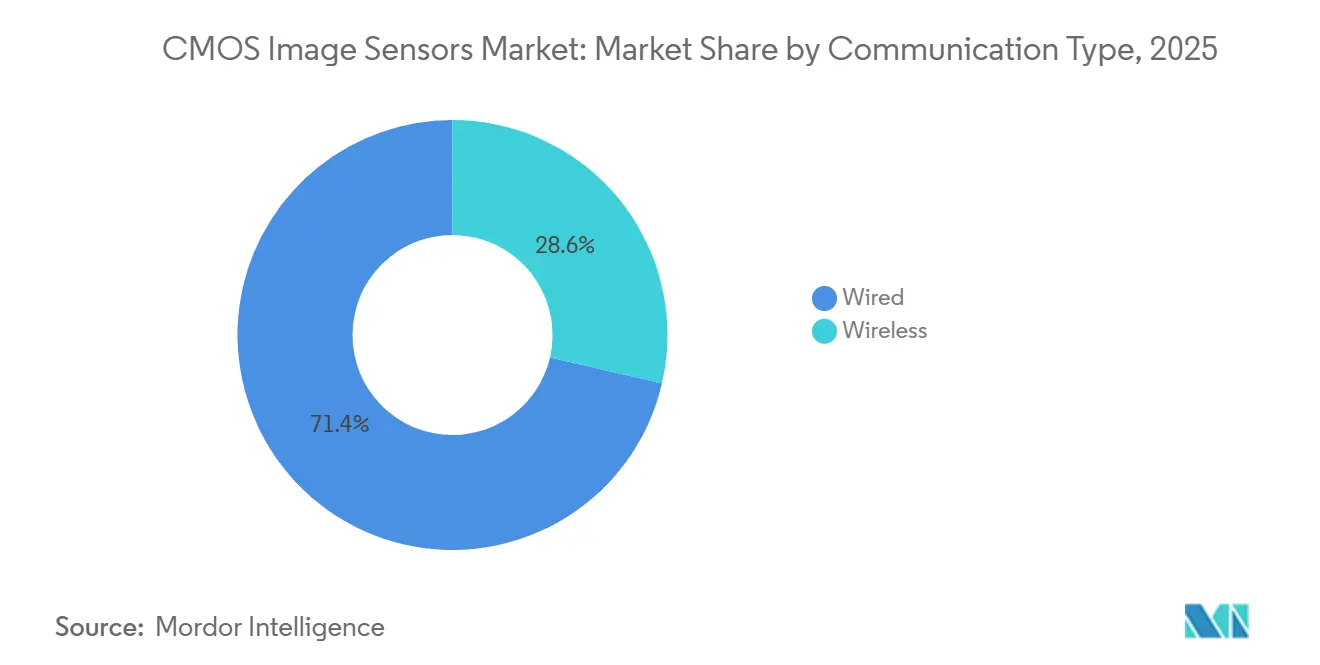
- By communication type, wired interfaces held 71.38% share in 2025, whereas wireless sensor modules are expected to post a 7.81% CAGR to 2031.
- By end-user, consumer electronics commanded 51.82% revenue in 2025 and automotive is set to record the fastest 8.22% CAGR between 2026 and 2031.
- By geography, Asia-Pacific commanded 63.93% of the market revenue in 2025, while the Middle East is projected to register the fastest CAGR of 7.33% between 2026 and 2031.
Note: Market size and forecast figures in this report are generated using Mordor Intelligence’s proprietary estimation framework, updated with the latest available data and insights as of 2026.
Global CMOS Image Sensors Market Trends and Insights
Drivers Impact Analysis*
| Driver | (~) % Impact on CAGR Forecast | Geographic Relevance | Impact Timeline |
|---|---|---|---|
| Smartphone Multi-Camera Adoption by Asia-Pacific OEMs | +1.20% | Asia-Pacific (China, India, South Korea), spillover to global premium segments | Medium term (2-4 years) |
| Regulatory Mandates for ADAS Cameras in United States and European Union | +1.50% | North America and Europe, with OEM supply chains extending to Asia-Pacific manufacturing hubs | Long term (≥4 years) |
| Video-Centric Social Media Demand for 4K and 8K Sensors in North America | +0.80% | North America, Europe, emerging creator economies in Latin America and Southeast Asia | Short term (≤2 years) |
| Miniaturized Sensors for Wearable Medical Imaging in Japan and European Union | +0.60% | Japan, European Union (Germany, France, United Kingdom), United States research institutions | Long term (≥4 years) |
| Smart-City Surveillance Roll-Outs in Middle East | +0.50% | Middle East (Saudi Arabia, United Arab Emirates, Israel), spillover to Africa and South Asia | Medium term (2-4 years) |
| Global-Shutter Demand for Industrial Automation in Germany's Industry 4.0 | +0.70% | Europe (Germany, Italy, France), North America, Asia-Pacific manufacturing corridors | Medium term (2-4 years) |
| Source: Mordor Intelligence | |||


Smartphone Multi-Camera Adoption by Asia-Pacific OEMs
Asia-Pacific brands embedded an average of 4.2 CMOS sensors per flagship handset in 2025, up from 2.8 in 2020, as computational photography demanded ultra-wide, telephoto, macro, and depth modules. Chinese vendors Xiaomi, OPPO, and Vivo shipped 42% of global smartphones in 2025, each specifying 50–200-megapixel sensors to stand out in a saturated field.[1]Amy Fan and Sherri Wang, “Samsung wins Apple iPhone image sensor deal in Texas, eyes Qualcomm next,” DIGITIMES Asia, digitimes.com The rising camera count offsets the modest 3%-unit CAGR expected through 2030, enlarging bill-of-materials value even as replacement cycles lengthen. SmartSens introduced the SC530AT 5-megapixel sensor with 100 decibels stacked HDR for in-cabin monitoring, showing how phone-style multi-sensor architectures migrate into automotive cabins. Samsung’s outsourcing of overflow production to UMC underscores foundry tightness and the race to match Sony’s scale.
Regulatory Mandates for ADAS Cameras in United States and European Union
The United States Federal Motor Vehicle Safety Standard 127, finalized in 2024, requires automatic emergency braking on all new light vehicles by September 2029 and implies at least five CMOS sensors per car.[2]National Highway Traffic Safety Administration, “NHTSA Finalizes Rule Requiring Automatic Emergency Braking Technology on New Vehicles,” nhtsa.gov Europe’s General Safety Regulation, effective July 2024, sets parallel obligations. Automakers must therefore validate sensors under ISO 26262 and lock multi-year supply contracts, removing price as the primary filter and shifting rivalry toward quantum efficiency at 940 nanometers. Sony has targeted a doubling of automotive revenue by 2028 through alliances with Continental and Bosch. Near-infrared performance and cybersecurity features such as image authentication now differentiate bidding suppliers.
Video-Centric Social Media Demand for 4K and 8K Sensors in North America
Content creators uploaded more than 720 million hours of 4K video in 2025, a 38% jump from 2024, because platform algorithms reward high-resolution footage. CMOS sensors enabling stable 4K60 capture with on-chip stabilization, therefore moved from cinema rigs into advanced smartphones and mirrorless vlogging cameras. RED Digital Cinema’s 8K products and Canon’s 410-megapixel prototype prove that extreme resolution no longer compromises frame rate, foreshadowing consumer trickle-down within five years.[3]U.S. Canon Inc., “Canon Develops CMOS Sensor with 410 Megapixels, the Largest Number of Pixels Ever Achieved in a 35 mm Full-frame Sensor,” usa.canon.com Demand for backside-illuminated architectures that preserve image quality in varied lighting continues to rise among independent creators.
Smart-City Surveillance Rollouts in Middle East
Riyadh installed over 1,600 AI-enabled cameras in November 2025, each built around a 5-megapixel CMOS sensor integrated with edge neural processors, cutting bandwidth costs by 80% versus legacy designs. The United Arab Emirates earmarked USD 2.4 billion to deploy 50,000 networked cameras by 2027 under ISO/IEC 27001 security rules. Suppliers that bundle sensors, processors, and wireless links in a turnkey module win procurement bids, an approach pursued by SmartSens and GalaxyCore with regional integrators.
Restraints Impact Analysis*
| Restraint | (~) % Impact on CAGR Forecast | Geographic Relevance | Impact Timeline |
|---|---|---|---|
| Advanced 300-mm CIS Wafer Capacity Constraints in Taiwan and South Korea | -0.90% | Global, with acute pressure in Asia-Pacific foundry hubs (Taiwan, South Korea) | Medium term (2-4 years) |
| Average Selling Price Erosion in Entry-Level Smartphones | -0.70% | Global, most pronounced in Asia-Pacific and emerging markets (India, Southeast Asia, Africa) | Short term (≤2 years) |
| Thermal Noise and Rolling-Shutter Limits in High-Speed Cinematography | -0.40% | North America, Europe (professional cinema and broadcast segments) | Long term (≥4 years) |
| United States-China Export Controls on Leading-Edge CIS | -0.80% | Global supply chains, with direct impact on China and indirect effects on Asia-Pacific and North America OEMs | Medium term (2-4 years) |
| Source: Mordor Intelligence | |||
Advanced 300-mm CIS Wafer Capacity Constraints in Taiwan and South Korea
Taiwan Semiconductor Manufacturing Company and Samsung Foundry supplied 68% of 300 mm CIS wafers in 2025 but prioritized higher-margin logic, creating a gap of 25,000 wafer starts per month versus demand through 2027. Lead times lengthened to 20 weeks, delaying handset launches and automotive validation. Tower Semiconductor has committed USD 1.2 billion to add 15,000 wafer starts in Israel by Q4 2027, yet tight capacity still channels market share toward vertically integrated players with captive fabs.
Average Selling Price Erosion in Entry-Level Smartphones
Sensors priced below USD 3 represented 52% of units but only 18% of revenue in 2025, as average prices in the sub-12-megapixel class fell 14% year-over-year. Chinese module makers Sunny Optical and O-Film compete on razor-thin margins, squeezing second-tier vendors that lack economies of scale. OmniVision, under Will Semiconductor, is therefore refocusing on premium sockets that support 40% higher average selling prices, although at lower volumes.
*Our forecasts treat driver/restraint impacts as directional, not additive. The impact forecasts reflect baseline growth, mix effects, and variable interactions.
Segment Analysis
By Technology: Stacked Designs Propel On-Chip Intelligence
Backside-illuminated devices led the CMOS image sensors market share at 55.45% in 2025. Stacked BSI and 3-D architectures are expected to deliver a 7.84% CAGR by embedding neural engines and DRAM within the die stack, shrinking system footprints without sacrificing frame rate. Sony’s IMX927 global-shutter sensor achieves 8 frames per second at 105 megapixels, proving that copper-pillar bonding can combine pixel layers with logic at production volumes. Canon demonstrated 3,280 megapixels-per-second readouts in a 410-megapixel full-frame device, underscoring the bandwidth advantage of layer separation. Front-side-illuminated parts persist in cost-sensitive webcams and barcode scanners where quantum efficiency above 50% suffices. Global-shutter CMOS, priced around USD 18 per 2-megapixel industrial unit, gains favour in Industry 4.0 plants that demand distortion-free inspection at conveyor speeds beyond 10 m/s. As on-chip intelligence climbs, vertically integrated suppliers that own both sensor and processor IP stand to widen margins across the CMOS image sensors market.
Stacked architectures yield heterogeneous integration, pairing 65 nm logic layers with 90 nm photodiode tiers for optimal trade-offs. Osaka City University’s three-wafer prototype with an embedded deep neural network circuit cut edge-processing power draw by 60% versus external ISPs. These advances accelerate adoption in surveillance drones, augmented-reality headsets, and implantable medical devices, segments that prize performance per milliwatt. In the CMOS image sensors market, capacity constraints on advanced wafer bonding elevate barrier-to-entry, thus concentrating value among leaders that master both process integration and in-house algorithm design.


By Resolution: Ultra-High Pixels Enable Computational Cropping
The 12–24-megapixel class captured 47.29% of 2025 revenue in the CMOS image sensors market, driven by mid-range smartphones balancing file size and optical design headroom. Sensors above 49 megapixels will expand at 7.25% CAGR because surveillance, medical imaging, and industrial inspection use digital zoom to replace mechanical movement. Canon’s 410-megapixel device allows operators to extract any 4K window while retaining broadcast clarity, consolidating camera counts by 40% in smart-city deployments. Sub-12-megapixel parts remain dominant in automotive surround-view modules where 60 fps low-light performance matters more than pixel density.
Sony’s 5-megapixel IMX775 sensor with 2.1 µm pixels shows how moderate resolution marries high near-infrared sensitivity for driver monitoring. Economies of scale in 12–24-megapixel optics suppress cost, sustaining dominance in smartphones and drones. Nonetheless, yield challenges on die size push ultra-high-resolution makers toward sub-1.4 µm pixels and advanced fault screening, reinforcing the importance of mature lithography nodes. The CMOS image sensors market size for ultra-high pixels will therefore hinge on balancing defect density, lens complexity, and system-level processing overhead.
By Spectrum: Non-Visible Bands Unlock New Modalities
Visible-light sensors held 68.14% revenue in 2025, yet non-visible variants spanning near-infrared, ultraviolet, and short-wave infrared are predicted to record a 7.56% CAGR. Sony’s IMX775 merges RGB and 940 nm NIR capture on one die, cutting vehicle bill-of-materials by USD 8 and ensuring co-registered colour and depth data. Short-wave infrared sensors using indium gallium arsenide now top 80% quantum efficiency at 1,550 nm, enabling moisture detection and photovoltaic inspection. Ultraviolet devices power lithography metrology and fluorescence microscopy.
Hybrid bonding of III-V materials raises cost and process complexity, but automotive volume ramps will cut non-visible sensor prices by 30% between 2025 and 2028. As machine-vision buyers demand multispectral data in a single housing, suppliers that integrate colour, NIR, and depth layers will secure design wins, enlarging the CMOS image sensors market size across precision agriculture, logistics, and contactless biometrics.
By Communication Type: Wireless Enables Untethered Edge Devices
Wired interfaces such as MIPI CSI-2 kept 71.38% share in 2025 because deterministic latency under 10 µs satisfies automotive and industrial safety requirements. Wireless CMOS modules are forecast to grow 7.81% CAGR as wearable health monitors, drones, and distributed cameras avoid costly cabling. Asahi Kasei’s AIMEZ module transmits posture data at 2.5 Mbps over 48 cm while consuming just 2.6 mW, legitimizing battery-powered elder-care devices. Capsule endoscopes already embed 320×240 CMOS sensors with RF links, eliminating infection-prone wires.
Automotive remains wired because ISO 26262 mandates redundancy and electromagnetic immunity. MIPI CSI-2 v4.0 now reaches 32 Gbps over 16 lanes, easily accommodating 8K video. Laboratory terahertz links achieved 10 Gbps over 10 m in 2025, hinting at future wireless parity. For now, the CMOS image sensors market embraces a hybrid model: wired in latency-critical environments and wireless where mobility, maintenance cost, or medical safety dominate.
By End-User Industry: Automotive Surges on Safety Regulations
Consumer electronics still led revenue with 51.82% in 2025, yet automotive will post the fastest 8.22% CAGR through 2031. Federal Motor Vehicle Safety Standard 127 compels every new U.S. light vehicle after 2029 to integrate automatic emergency braking supported by at least five CMOS cameras. European mandates mirror this momentum. Sony’s IMX775 and SmartSens’s SC530AT meet AEC-Q100 Grade 2 and ISO 26262 ASIL-B levels, reflecting the new baseline for in-cabin driver monitoring.
Industrial automation stresses global-shutter parts for robotic pick-and-place, while healthcare pioneers miniature implantable cameras capturing neural activity. As premium phones stretch replacement cycles, rising camera counts offset volume slack, keeping consumer electronics central but ceding the growth crown to automotive within the CMOS image sensors market.
Geography Analysis
Asia-Pacific commanded 63.93% of 2025 revenue thanks to dominant wafer capacity at TSMC and Samsung Foundry and 42% global smartphone shipments from Chinese OEMs. Sony maintained over 60% smartphone sensor share and incubates stacked neural solutions in Japan. Samsung’s 2027 Apple contract in Austin highlights geographic diversification away from geopolitical risk. India’s 180-million-unit handset market drives entry-level sensor volume, although ASP erosion compresses margins. The Middle East will be the fastest riser with a 7.33% CAGR to 2031, fuelled by Riyadh’s 1,600-camera rollout and the UAE’s USD 2.4 billion smart-city program.
North America gains from mandatory ADAS adoption and a booming creator economy uploading 4K and 8K content. Europe pushes global-shutter demand for Industry 4.0 robotics, with Siemens and Bosch specifying 10 µs exposure ceilings.
Africa and South America together remain under 8% of revenue yet present volume upside in mobile-first economies adopting sub-USD 150 smartphones. Overall, wafer capacity bottlenecks in Asia-Pacific and rising capital outlays in Israel and the United States reshape the supply map of the CMOS image sensors market.

Competitive Landscape
Sony, Samsung, and OmniVision captured an estimated 74% of 2025 revenue, making the CMOS image sensors market highly consolidated. Sony’s exploration of a USD 35-49 billion spin-off signals pressure to unlock value as smartphone growth slows.
Samsung’s one-stop design-to-fab model, anchored by a Texas facility for Apple and potential expansion to Qualcomm, challenges Sony’s leadership. Chinese challengers SmartSens and GalaxyCore ride automotive and surveillance niches, offering AEC-Q100 sensors at a 20% discount to incumbents. Canon advances ultra-high-resolution stacked sensors while Tower Semiconductor’s USD 1.2 billion capacity build targets customers seeking guaranteed 300 mm supply.
Patent portfolios fortify incumbents: Sony holds more than 4,200 CIS patents and Samsung filed 890 new applications during 2024-2025, raising entry hurdles. Foundry scarcity forces fabless players to secure long-term allocations or exit commodity tiers. Emerging white space lies in short-wave infrared and ultraviolet imaging, where III-V integration expertise trumps scale. As R&D costs for stacked BSI architectures rise, further consolidation is likely, with vertical integration favoured for margin defense in the CMOS image sensors market.
CMOS Image Sensors Industry Leaders
Sony Group Corporation
Samsung Electronics Co., Ltd.
OmniVision Technologies, Inc.
onsemi Corporation
STMicroelectronics N.V.
- *Disclaimer: Major Players sorted in no particular order

Recent Industry Developments
- June 2025: Sony Semiconductor Solutions announced the LYT-828, a 50-megapixel CMOS image sensor featuring dynamic range exceeding 100 dB and Hybrid Frame-HDR technology, scheduled for mass production in late August 2025 to enhance smartphone imaging capabilities in high-contrast scenes.
- April 2025: OmniVision launched a 1.5-megapixel global shutter sensor specifically designed for automotive driver monitoring systems, expanding the company's presence in automotive safety applications.
- April 2025: TSMC's Arizona facility accelerated expansion plans with a USD 165 billion investment to house six fabs, with the first fab utilizing 4nm technology for high-end SoCs and subsequent fabs planned for 3nm and 2nm technologies.
- March 2025: onsemi introduced the Hyperlux ID family, the first real-time indirect time-of-flight sensor capable of high precision depth measurements up to 30 meters for industrial automation applications.


Global CMOS Image Sensors Market Report Scope
The CMOS Image Sensors Market Report is Segmented by Technology (Front-Side Illuminated, Backside-Illuminated, Stacked BSI/3-D, Global-Shutter CMOS), Resolution (Less than 12 Megapixels, 12-24 Megapixels, 25-48 Megapixels, Greater than 49 Megapixels), Spectrum (Visible, Non-Visible), Communication Type (Wired, Wireless), End-User Industry (Consumer Electronics, Automotive, Industrial, Security, Healthcare, Computing, Aerospace), and Geography (North America, Europe, Asia-Pacific, Middle East, Africa, South America). Market Forecasts are Provided in Terms of Value (USD).
| Front-Side Illuminated (FSI) |
| Backside-Illuminated (BSI) |
| Stacked BSI / 3-D |
| Global-Shutter CMOS |
| Less than 12 Megapixels |
| 12-24 Megapixels |
| 25-48 Megapixels |
| Greater than 49 Megapixels |
| Visible Spectrum |
| Non-Visible (NIR, UV, SWIR) Spectrum |
| Wired |
| Wireless |
| Consumer Electronics |
| Automotive and Transportation |
| Industrial and Machine Vision |
| Security and Surveillance |
| Healthcare and Life Sciences |
| Computing and Data-Center |
| Aerospace and Defense |
| North America | United States |
| Canada | |
| Mexico | |
| Europe | United Kingdom |
| Germany | |
| France | |
| Italy | |
| Rest of Europe | |
| Asia-Pacific | China |
| Japan | |
| India | |
| South Korea | |
| Rest of Asia-Pacific | |
| Middle East | Israel |
| Saudi Arabia | |
| United Arab Emirates | |
| Turkey | |
| Rest of Middle East | |
| Africa | South Africa |
| Egypt | |
| Rest of Africa | |
| South America | Brazil |
| Argentina | |
| Rest of South America |
| By Technology | Front-Side Illuminated (FSI) | |
| Backside-Illuminated (BSI) | ||
| Stacked BSI / 3-D | ||
| Global-Shutter CMOS | ||
| By Resolution | Less than 12 Megapixels | |
| 12-24 Megapixels | ||
| 25-48 Megapixels | ||
| Greater than 49 Megapixels | ||
| By Spectrum | Visible Spectrum | |
| Non-Visible (NIR, UV, SWIR) Spectrum | ||
| By Communication Type | Wired | |
| Wireless | ||
| By End-User Industry | Consumer Electronics | |
| Automotive and Transportation | ||
| Industrial and Machine Vision | ||
| Security and Surveillance | ||
| Healthcare and Life Sciences | ||
| Computing and Data-Center | ||
| Aerospace and Defense | ||
| By Geography | North America | United States |
| Canada | ||
| Mexico | ||
| Europe | United Kingdom | |
| Germany | ||
| France | ||
| Italy | ||
| Rest of Europe | ||
| Asia-Pacific | China | |
| Japan | ||
| India | ||
| South Korea | ||
| Rest of Asia-Pacific | ||
| Middle East | Israel | |
| Saudi Arabia | ||
| United Arab Emirates | ||
| Turkey | ||
| Rest of Middle East | ||
| Africa | South Africa | |
| Egypt | ||
| Rest of Africa | ||
| South America | Brazil | |
| Argentina | ||
| Rest of South America | ||


Key Questions Answered in the Report
What is the projected value of the CMOS image sensors market in 2031?
It is forecast to reach USD 36.96 billion by 2031, expanding at a 6.99% CAGR from 2026.
Which end-user segment will grow fastest through 2031?
Automotive, supported by mandatory automatic emergency braking rules in the United States and Europe, is expected to post an 8.22% CAGR.
How many cameras will a typical light vehicle need to meet new U.S. safety rules?
Base models will require at least five CMOS cameras to comply with Federal Motor Vehicle Safety Standard 127.
Why are stacked CMOS sensors important?
Stacked architectures embed neural processors and DRAM within the sensor, boosting frame rate and efficiency without enlarging die size.
Which region currently leads production of CMOS image sensors?
Asia-Pacific controls nearly two-thirds of global revenue thanks to extensive foundry capacity and dominant smartphone OEMs.
What technology challenge constrains future supply?
Limited 300 mm wafer capacity for advanced stacked sensors in Taiwan and South Korea lengthens lead times and favors vertically integrated players.
Page last updated on:


