
Ceramic Substrate Market Size and Share
Market Overview
| Study Period | 2021 - 2031 |
|---|---|
| Market Size (2026) | USD 6.88 Billion |
| Market Size (2031) | USD 9.44 Billion |
| Growth Rate (2026 - 2031) | 6.54 % |
| Fastest Growing Market | Asia Pacific |
| Largest Market | Asia Pacific |
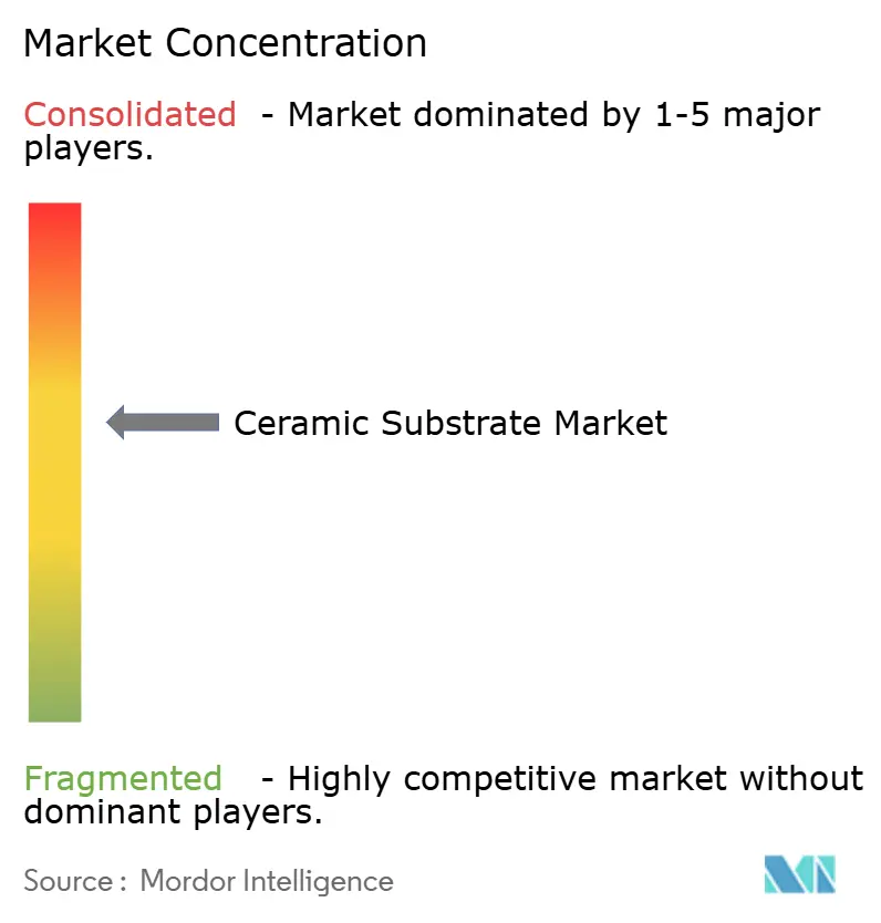
| Market Concentration | Medium |
Major Players *Disclaimer: Major Players sorted in no particular order Image © Mordor Intelligence. Reuse requires attribution under CC BY 4.0. | |
Ceramic Substrate Market Analysis by Mordor Intelligence
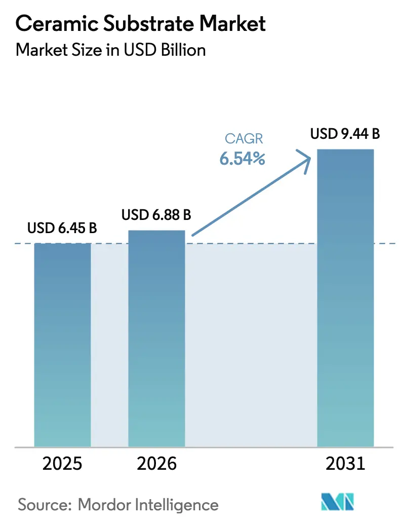
The Ceramic Substrate Market size is projected to expand from USD 6.45 billion in 2025 and USD 6.88 billion in 2026 to USD 9.44 billion by 2031, registering a CAGR of 6.54% between 2026 to 2031. Market momentum is shifting from passive heat-spreading roles toward active enablement of silicon-carbide and gallium-nitride power devices that tolerate junction temperatures above 200°C, conditions under which organic laminates fail within months. Automotive traction inverters, 5G radio-frequency (RF) modules, and aerospace phased-array radars are the principal demand vectors, supported by rising wide-bandgap wafer output in Asia-Pacific. Competitive strategies emphasize vertical integration to compress supply chains, while policy tailwinds, such as the United States Inflation Reduction Act and the European Union Carbon Border Adjustment Mechanism, anchor new capacity investments. Together, these dynamics ensure that the ceramic substrate market will remain on a solid mid-single-digit growth trajectory through 2031.
Key Report Takeaways
- By type, alumina captured 44.18% of the ceramic substrate market share in 2025, whereas silicon carbide substrates are projected to expand at a 7.80% CAGR to 2031.
- By manufacturing process, low-temperature co-fired ceramic (LTCC) accounted for 36.86% of revenue in 2025; active-metal-brazed (AMB) substrates are forecast to rise at a 7.10% CAGR through 2031.
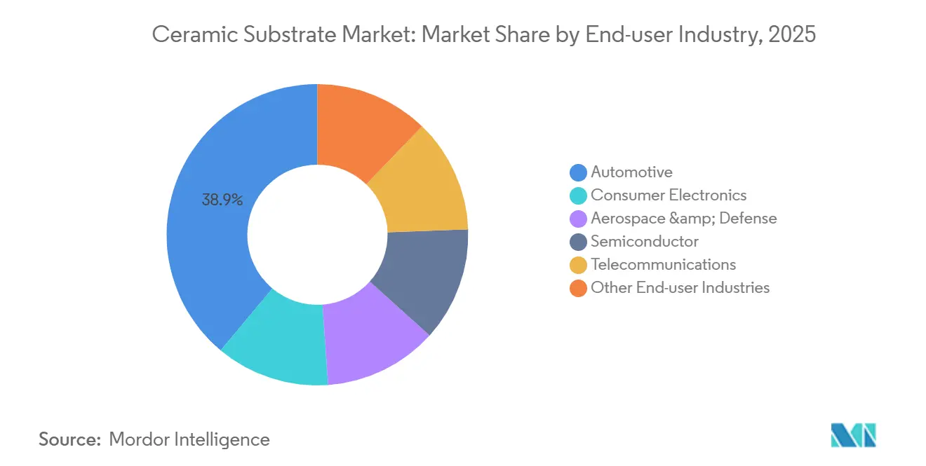
- By end-user industry, automotive held a 38.92% share in 2025, while the other end-user industries are poised to lead growth with an 8.40% CAGR to 2031.
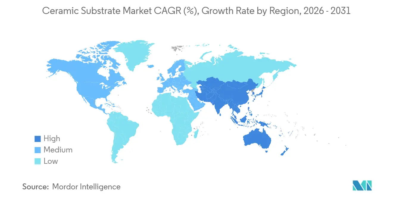
- By geography, Asia-Pacific commanded 46.61% of global revenue in 2025 and is expected to maintain the fastest regional CAGR of 7.09% over the outlook period.
Note: Market size and forecast figures in this report are generated using Mordor Intelligence’s proprietary estimation framework, updated with the latest available data and insights as of January 2026.
Global Ceramic Substrate Market Trends and Insights
Drivers Impact Analysis*
| Driver | (~) % Impact on CAGR Forecast | Geographic Relevance | Impact Timeline |
|---|---|---|---|
| Superior thermal conductivity enabling high-power electronics | +1.8% | Global, strongest in Asia-Pacific and North America | Medium term (2-4 years) |
| Rapid EV inverter and on-board-charger build-out | +2.1% | Asia-Pacific core, spillover to Europe and North America | Short term (≤2 years) |
| 5G base-station and RF module densification | +1.3% | Global, led by Asia-Pacific and North America | Short term (≤2 years) |
| SiC/GaN migration requiring AlN and DBC substrates | +1.0% | North America & Europe for aerospace; Asia-Pacific for automotive | Medium term (2-4 years) |
| Aerospace CubeSat miniaturization needs LTCC | +0.4% | North America and Europe, niche in Asia-Pacific | Long term (≥4 years) |
| Source: Mordor Intelligence | |||
Superior Thermal Conductivity Enabling High-Power Electronics
Designers now treat thermal conductivity as a primary constraint rather than a secondary specification. Silicon-carbide MOSFETs and gallium-nitride HEMTs run at junction temperatures up to 225°C, generating local heat fluxes that top 300 W/cm², well beyond the safe envelope for epoxy-based laminates[1]Rogers Corporation, “Power Electronics Substrate Materials,” rogerscorp.com. Aluminum-nitride substrates, offering 170–250 W/m·K, cut heat-sink volume by 35% and trim liquid-coolant flow rates, improving full-system efficiency by 2–3%. Direct-bonded-copper (DBC) variants eliminate adhesive layers, slicing thermal resistance by 0.1 K·cm²/W and allowing current densities of 200 A/cm² in automotive traction inverters. Multi-company investments that will lift global SiC wafer output from 150-mm to 200-mm diameters further expand the ceramic substrate market.
Rapid EV Inverter and On-Board-Charger Build-Out Increasing Usage
Battery-electric vehicles are standardizing on 800-V architectures, which impose voltage transients above 1,200 V and thermal cycling from −40°C to 150°C over 200,000 cycles. To meet these conditions, automakers integrate DBC substrates that handle regenerative-braking reversals within milliseconds, loads that fracture FR-4 boards. Silicon-carbide diodes on aluminum-nitride bases lift on-board-charger efficiency to 98% and shave cooling-system mass by 20%, extending vehicle range. Kyocera’s USD 454 million Nagasaki build-out will double automotive-grade substrate capacity by late 2026. As module costs fall, premium-segment penetration already exceeds 80%, and mainstream adoption is tracking downward cost curves, cementing demand for the ceramic substrate market.
5G Base-Station and RF Module Densification
Telecom equipment suppliers employ LTCC to embed inductors, capacitors, and transmission lines inside multilayer stacks, shrinking RF front-end volume by 40% and slicing insertion loss by 0.5 dB at 28 GHz[2]Fraunhofer IZM, “LTCC for 5G RF Front Ends,” fraunhofer.de. Massive-MIMO platforms deploying up to 256 antenna elements per sector need dielectric-loss tangents below 0.001; LTCC and high-temperature co-fired ceramics are the only proven commercial options. Asia-Pacific operators rolling out standalone 5G networks are driving continuous call-offs, propelling the ceramic substrate market through 2031.
SiC/GaN Migration Requiring AlN and DBC Substrates
Wide-bandgap semiconductors exhibit coefficients of thermal expansion near 4.5 ppm/K, aligning closely with aluminum nitride and mitigating solder-joint fatigue. DBC on AlN accommodates 0.6-mm copper traces without warpage, enabling 400 A continuous currents in EV traction inverters. Aerospace radar arrays also demand dimensional stability across −55°C to 125°C, directing specifications toward AlN.
Restraints Impact Analysis*
| Restraint | (~) % Impact on CAGR Forecast | Geographic Relevance | Impact Timeline |
|---|---|---|---|
| High price premium over metal/organic boards | −0.9% | Global, acute in cost-sensitive consumer electronics | Short term (≤2 years) |
| Fragility and yield losses during assembly | −0.5% | Global, concentrated in high-volume automotive & consumer lines | Medium term (2-4 years) |
| Toxic-exposure limits on BeO | −0.2% | North America and Europe | Long term (≥4 years) |
| Source: Mordor Intelligence | |||
High Price Premium Over Metal/Organic Boards
Unit prices range from USD 2 to USD 10 per square inch versus USD 0.10–0.50 for FR-4, a 5-to-20-fold spread that shuts entry into many consumer devices. Raw alumina powder and metallization account for 60% of the cost, while yield loss contributes another 15%, leaving scant room for markdowns without process innovation. Temporary shortages in 2024–2025 inflated prices by up to 20%, compelling some handset makers to revert to metal-core PCBs. Hybrid assemblies that place ceramic only under high-heat-flux components cut substrate spend by 30% while retaining most thermal benefit.
Fragility and Yield Losses During Assembly
Flexural strengths of 300–500 MPa make ceramics prone to edge chipping and thermal-shock cracking during reflow, where ramps from 25°C to 260°C occur within one minute. Coefficient-of-expansion mismatch between silicon, ceramics, and copper elevates shear stress, shortening module life by 20% in accelerated tests. Automotive lines report 5–15% scrap, concentrated in laser-scribing and die-attach stations. Automated optical inspection and robotic handling have trimmed defect rates by 30% since 2023, yet brittleness remains an intrinsic constraint that caps the attainable CAGR for the ceramic substrate market.
*Our forecasts treat driver/restraint impacts as directional, not additive. The impact forecasts reflect baseline growth, mix effects, and variable interactions.
Segment Analysis
By Type: Alumina Retains Volume Leadership Amid SiC Advancement
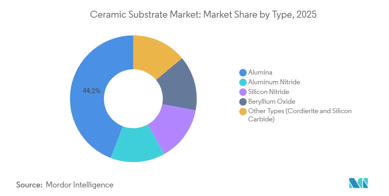
Alumina delivered 44.18% of the ceramic substrate market share in 2025, anchored by cost-sensitive consumer electronics and industrial drives. At the same time, silicon carbide substrates expanded 7.80% CAGR through 2031, propelled by aerospace radars and next-generation EV inverters that require coefficient-of-thermal-expansion mismatches below 0.5 ppm/K. Aluminum nitride, with 170–250 W/m·K conductivity, is gaining traction in 800-V EV platforms where operating junctions exceed 175°C.
Revenue momentum favors premium materials because average selling prices remain three to five times higher than alumina equivalents. As Coherent, DENSO, and Mitsubishi Electric pour USD 1 billion into 200-mm SiC wafer lines, downstream demand for compatible substrates will accelerate, reshaping the ceramic substrate market size profile. Alumina will keep its volume edge through 2031 in LEDs and smartphone power-management ICs, yet its revenue share will slip as telecom and data-center designers upgrade to AlN for lower dielectric loss.



By Manufacturing Process: LTCC Dominates While AMB Gains Momentum
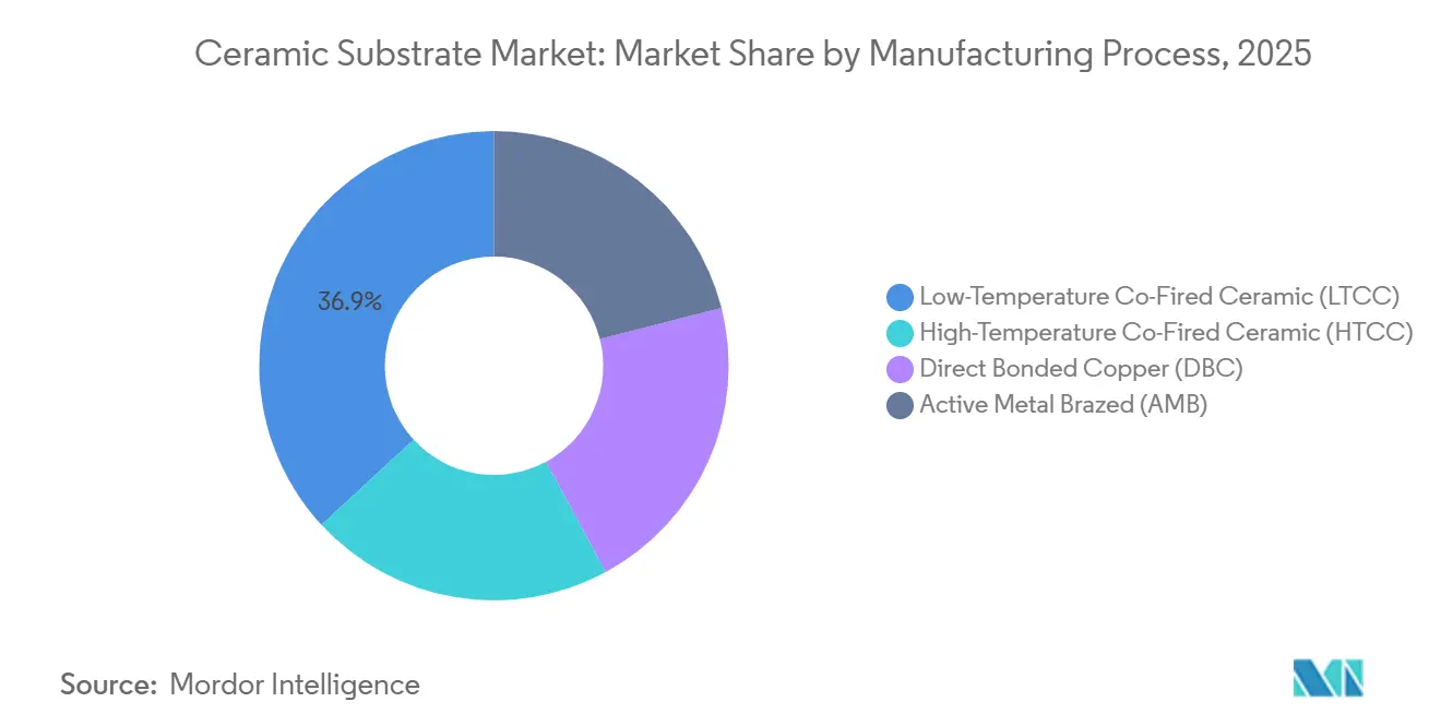
Low-Temperature Co-Fired Ceramic (LTCC) secured 36.86% of 2025 revenue by embedding passives into multilayer stacks that cut RF module footprints by 40%. Active Metal Brazed (AMB) substrates are poised for a 7.10% CAGR because titanium-based brazing removes nickel interlayers, shaving 0.05 K·cm²/W from thermal resistance and extending power-module life by 5%.
High-Temperature Co-Fired Ceramic (HTCC) retains a niche for avionics requiring dielectric strength above 10 kV/mm, but its cost structure is 30% higher than LTCC due to 1,600°C firing temperatures. DBC remains the workhorse in EV traction inverters that cycle 50 times per second between −40°C and 150°C, sustaining steady mid-single-digit growth for the ceramic substrate market.
By End-User Industry: Automotive Leads, Renewables Accelerate
Automotive applications generated 38.92% of 2025 revenue, anchored by 800-V traction inverters that rely on DBC substrates to manage regenerative-braking spikes. Renewable-energy and industrial-power sectors, grouped under other, are projected to rise 8.40% annually to 2031 as solar-farm inverters and offshore wind converters migrate to SiC devices on aluminum nitride (AlN) bases, pushing the ceramic substrate market size higher.
Consumer electronics stay in second place by volume, yet growth lags as handset makers shift to cheaper metal-core boards with thermal vias. Medical implants and aerospace radar modules, small but lucrative niches, command premium unit prices exceeding USD 100 per substrate, reinforcing a barbell revenue structure for the ceramic substrate industry.
Geography Analysis
Asia-Pacific contributed 46.61% of revenue in 2025 and is expected to post a 7.09% CAGR through 2031, buoyed by Chinese EV output topping 9 million units in 2024 and Japanese initiatives to triple translucent-alumina wafer capacity by fiscal 2027. Kyocera’s Nagasaki complex, slated for late 2026 completion, will co-locate SiC substrate and advanced packaging lines, cutting lead times by 30% and reinforcing regional self-sufficiency.
North America’s 2025 share was driven by defense and space programs that specify AlN substrates for phased-array radars operating across −55°C to 125°C. The Inflation Reduction Act’s clean-energy incentives underpin domestic inverter assembly, cushioning slower EV penetration relative to Asia.
In Europe, high energy prices inflate alumina sintering costs by 25% versus Asia-Pacific, but the EU Carbon Border Adjustment Mechanism, phasing in USD 90-equivalent tariffs per ton of CO₂, nudges OEMs toward low-carbon alumina such as Hydro’s HalZero, lifting regional demand for recyclable substrates. South America and the Middle East & Africa remain sub-10% contributors; projects in Brazil’s solar belt and Saudi Arabia’s NEOM smart-city keep niche demand alive, yet import reliance raises landed cost by up to 25%, limiting the ceramic substrate market’s expansion there.

Value Chain Analysis
The ceramic substrate value chain begins with upstream feedstocks and consumables, mainly high-purity ceramic powders (Al2O3, AlN, Si3N4), metallization metals (notably copper and silver), and binders and solvents used in slurry and tape processes. Supply availability and pricing are shaped by the concentration of high-purity powder supply, while metallization and brazing consumables feed into DBC and AMB cost structures and can influence delivery timelines.
Midstream processing covers slurry preparation and tape casting, drying, lamination, and co-firing (LTCC and HTCC), followed by copper attachment through direct bonding or active metal brazing. After that, substrates go through dicing, inspection, and reliability screening. Kyocera and NGK illustrate a move toward vertically integrated footprints that combine ceramic forming and firing with downstream metallization and packaging-adjacent capabilities, which can reduce lead times and limit exposure to assembly yield losses. Downstream, substrates are qualified into power modules for EV traction inverters and industrial converters, LTCC-based RF front ends, aerospace electronics, and semiconductor manufacturing equipment, with distribution typically routed through direct OEM supply agreements and module or packaging integrators where qualification cycles and reliability standards influence switching costs.
Competitive Landscape
The Ceramic Substrate market is moderately consolidated. Vertical integration is the dominant play. Kyocera’s USD 454 million Nagasaki plant will integrate substrate firing, copper bonding, and semiconductor packaging by 2026, harvesting margin at two nodes of the value chain. NGK is tripling HICERAM alumina wafer output and boosting AMB/DBC capacity 2.5× by 2026 to secure JPY 20 billion in annual semiconductor sales. Process innovation is the challenger’s lever. Heraeus’ titanium-interlayer AMB stack trims thermal resistance by 0.05 K·cm²/W and has won design-ins at Bosch and Continental for 200–500 kW inverters. Looking ahead, quantum-computing and neuromorphic-chip projects seek cryogenic and mixed-signal substrates, opening new white-space territories for ceramic substrate industry participants.
Ceramic Substrate Industry Leaders
CoorsTek Inc.
KYOCERA Corporation
CeramTec GmbH
Rogers Corporation
TTM Technologies Inc.
- *Disclaimer: Major Players sorted in no particular order

Market Opportunities and Future Outlook
Opportunities are extending beyond traditional power-module heat-spreading into ceramic-core substrates for advanced semiconductor packages used in AI data center architectures. At higher layer counts and larger body sizes, organic substrate warpage becomes a practical constraint, which raises the value proposition for ceramics where stiffness and thermal stability support yield and performance.
Kyocera began commercialization of a multilayer ceramic core substrate for advanced AI semiconductor packages (xPUs and switch ASICs) in April 2026. On the supply side, investment is concentrating around ceramic components tied to semiconductor production and high-density computing. NGK announced a JPY 70 billion project in April 2026 to build a new plant in Nomi City, Ishikawa Prefecture, to increase capacity for ceramics used in semiconductor manufacturing equipment, and Kyocera communicated a large capital commitment to its components business in 2026 with emphasis on chipmaking and AI data center applications. In parallel, research around monolithic multilayer ceramic substrates for 800V SiC modules, additive metallization for near-chip functionalization, and lower-temperature copper film formation on Al2O3 points to whitespace in manufacturability and reliability, especially where interfaces and copper-ceramic adhesion need to support higher current density and thermal cycling endurance.
Recent Industry Developments
- July 2026: CoorsTek announced a USD 120 million investment to build the Center for Advanced Materials, a new advanced materials R&D facility in Golden, Colorado. The project targets higher R&D throughput for high-performance ceramics used across semiconductor and electronics supply chains, supporting faster development-to-qualification cycles for next-generation ceramic substrate and component applications.
- April 2026: Kyocera commercialized a multilayer ceramic core substrate for advanced AI semiconductor packages, targeting xPUs and switch ASICs used in AI data center architectures. By addressing warpage and package stability challenges that arise with large organic substrates, the commercialization extends ceramic substrates into higher-value advanced packaging use cases.
- August 2024: CoorsTek completed construction of its third factory in Gumi, Gyeongsangbuk-do, South Korea, to expand production of semiconductor equipment components. The additional manufacturing footprint supports more localized supply for Asia-based semiconductor ecosystems and reinforces capacity resilience for ceramic-based components that share upstream materials and processing with substrate manufacturing.


Research Methodology Framework and Report Scope
Market Definition and Coverage
This market covers the revenue generated from ceramic substrates used as base plates or circuit substrates in electronics and electrical applications where insulation and heat dissipation are required.
Scope exclusions: Packaging materials, metal leadframes, organic laminates, and bare semiconductor wafers are excluded from the market totals.
Segmentation Overview
- By Type
- Alumina
- Aluminum Nitride
- Silicon Nitride
- Beryllium Oxide
- Other Types (Cordierite andSilicon Carbide)
- By Manufacturing Process
- High-Temperature Co-Fired Ceramic (HTCC)
- Low-Temperature Co-Fired Ceramic (LTCC)
- Direct Bonded Copper (DBC)
- Active Metal Brazed (AMB)
- By End-User Industry
- Consumer Electronics
- Automotive
- Aerospace & Defense
- Semiconductor
- Telecommunications
- Other End-user Industries (Industrial Power & Renewable Energy, and Medical Devices)
- By Geography
- Asia-Pacific
- China
- India
- Japan
- South Korea
- Vietnam
- Malaysia
- Indonesia
- Thailand
- Rest of Asia-Pacific
- North America
- United States
- Canada
- Mexico
- Europe
- Germany
- United Kingdom
- France
- Italy
- Russia
- Turkey
- Spain
- NORDIC Countries
- Rest of Europe
- South America
- Brazil
- Argentina
- Colombia
- Rest of South America
- Middle East and Africa
- Saudi Arabia
- South Africa
- Qatar
- Nigeria
- United Arab Emirates
- Rest of Middle East and Africa
- Asia-Pacific
Data Sources, Market Sizing, and Validation
Desk Research
Desk work starts with building a fact base on electronics output and trade flows that influence ceramic substrate consumption. We typically reference public sources such as UN Comtrade for import and export patterns, the World Bank for macro indicators, the USGS for relevant minerals context, and the OECD for industrial production signals. For electronics manufacturing direction, we also use government statistics portals and customs releases where available.
After the macro and trade layer is set, we cross-check the market story using company annual reports, investor presentations, and reputable press coverage on capacity additions and technology shifts. When needed, paid subscriptions for company financials and intelligence, patent databases, and shipment-level import and export databases are used to validate product mix cues and timing of supply expansions. The desk sources listed above are illustrative, and many other public and paid sources were also used for data collection, validation, and clarification.
Primary Interviews and Surveys
Primary work focuses on confirming what drives real demand and pricing for ceramic substrates, especially across power electronics, telecom hardware, and industrial electronics. We speak with suppliers, distributors, and downstream users to validate adoption of different substrate materials and processes, and to stress-test assumptions on utilization, yield, and qualification cycles across regions.
Distribution of primary research fieldwork respondents
| Company type | Respondent position | Region |
|---|---|---|
| Top tier: 37% | CXOs: 12% | APAC: 46% |
| Mid tier: 46% | Functional/Unit leaders: 28% | EMEA: 32% |
| Smaller Players: 17% | Managers: 60% | Americas: 22% |
Market-Sizing & Forecasting
The sizing model starts from a top-down build where electronics and power module demand is reconstructed using production and trade signals, followed by material and process penetration rates to arrive at the ceramic substrate value pool. Results are then corroborated using selective bottom-up approximations, such as sampling supplier revenues where disclosed, channel checks on typical average selling prices, and volume to value conversions for high-usage applications.
Key inputs used in the model include the mix shift between alumina and higher thermal conductivity materials (such as aluminum nitride and silicon nitride), the split of HTCC and LTCC versus DBC and AMB routes, and the growth rate of end uses like automotive power electronics and telecom hardware. We also factor in capacity expansion timing, typical qualification lead times, and regional production concentration, since these affect short-term supply availability and realized pricing. Where bottom-up data is incomplete for smaller suppliers or private units, gaps are handled through peer benchmarking on product mix and estimated utilization, and then re-checked with interview feedback.
For forecasting, scenario analysis is used with a base case anchored to agreed demand drivers from experts, and sensitivity is run on substrate ASP progression and adoption rates in power modules. When a variable showed clear historical stability, exponential smoothing was applied to avoid overreacting to one-off spikes.
Data Validation & Update Cycle
Validation is done by comparing model outputs against independent signals, such as regional electronics production direction, trade movement for relevant ceramic components, and visible capacity announcements. If a region shows a jump that is not supported by these signals, the assumptions are reopened and respondents may be re-contacted to explain the variance before final sign-off.
Before publication, the model and assumptions go through multi-step analyst review so arithmetic, unit conversions, and currency handling are consistent across countries and years. Reports are refreshed annually, and interim updates are made when material events occur, such as major capacity start-ups, technology shifts in power devices, or sharp changes in input costs. Right before delivery, a fresh pass is performed so clients receive the most current view available.
Mordor Intelligence's Ceramic Substrate Market Size Versus Other Published Estimates
Different published market sizes for ceramic substrates can look far apart because the scope line is not drawn the same way, and because base years and pricing logic are not always aligned. We also see gaps when some studies assume aggressive penetration of high-end substrates into power electronics without confirming qualification timing and regional supply constraints.
Packaging substrates and organic laminates sit outside Mordor Intelligence's scope, which is one reason the 2026 value is lower than estimates that bundle adjacent electronics substrate categories and count a broader bill-of-materials basket. In addition, some publishers rely on a single base year price snapshot, while our model rechecks ASP movement using process mix (DBC and AMB versus HTCC and LTCC), end-use weighting, and currency timing so the value does not drift with short-term volatility.
Benchmark comparison
| Source | Market Size | Gaps in Research Methodology |
|---|---|---|
| Mordor Intelligence | USD 6.88 B (2026) | |
| Industry Research Publisher A | USD 8.54 B (2024) | Uses a 2024 base year and presents total sales value with a broader end-use basket, which can pull in adjacent substrate materials and earlier-year pricing that is not directly comparable to a 2026 valuation. |
| Market Research Publisher B | USD 8.49 B (2025) | Reports a 2025 base year and may apply faster adoption assumptions across end uses, which can lift the value if qualification cycles and regional capacity ramp timing are not explicitly constrained. |
The comparison shows that year selection and what gets counted as a ceramic substrate product can shift the total by a couple of billion dollars. By keeping the inclusions tied to ceramic substrates and then checking process mix, end-use demand signals, and price progression with interviews, the final number stays traceable and repeatable.


Key Questions Answered in the Report
What is the projected value of the ceramic substrate market in 2031?
The market is forecast to reach USD 9.44 billion by 2031.
Which material type commands the largest ceramic substrate market share today?
Alumina leads with a 44.18% share as of 2025.
Which segment is growing fastest within the ceramic substrate market?
Silicon carbide substrates are advancing at a 7.80% CAGR through 2031.
Why are ceramic substrates critical for 800-V electric-vehicle inverters?
They withstand over 1,200 V transients and 200,000 thermal cycles that would crack organic boards, enabling 150–350 kW fast charging.
How does LTCC benefit 5 G base-station designers?
How does LTCC benefit 5G base-station designers?
Page last updated on:


 Your data is secure and never sold or shared.


