
United States Semiconductor Manufacturing Equipment Market Size and Share
Market Overview
| Study Period | 2020 - 2031 |
|---|---|
| Forecast Data Period | 2026 - 2031 |
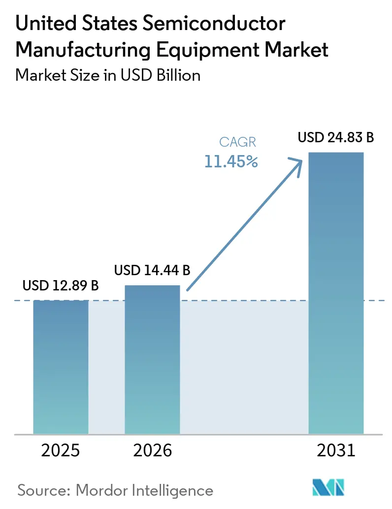
| Base Year Market Size (2025) | USD 12.89 Billion |
| Market Size (2026) | USD 14.44 Billion |
| Market Size (2031) | USD 24.83 Billion |
| Growth Rate (2026 - 2031) | 11.45 % |
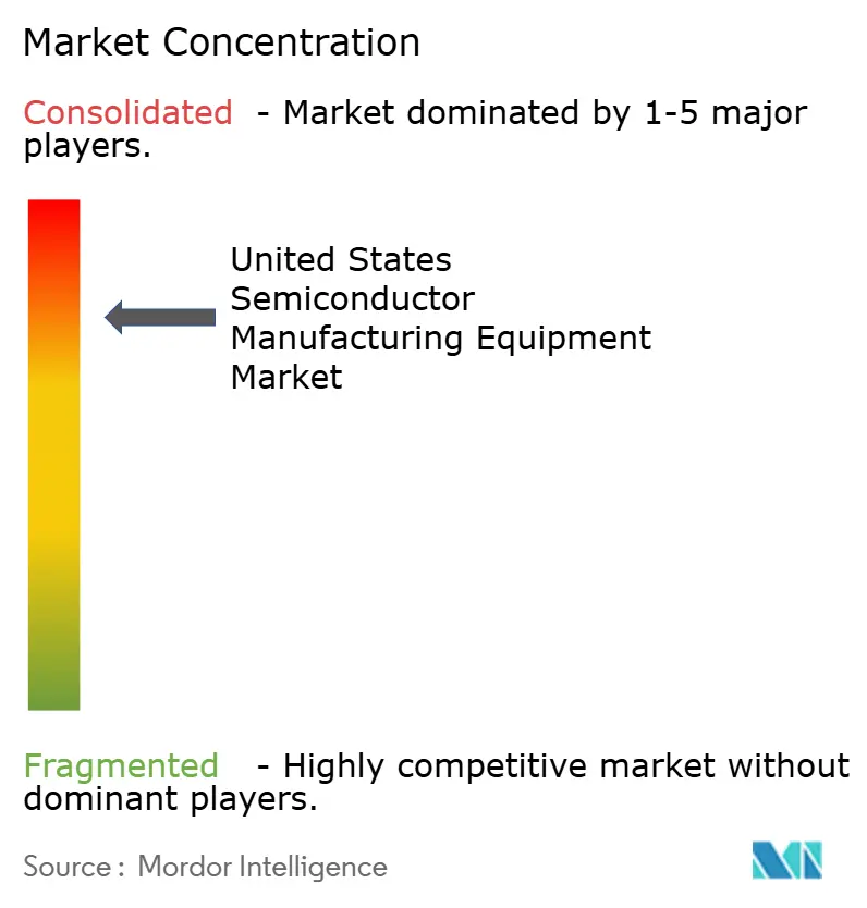
| Market Concentration | High |
Major Players *Disclaimer: Major Players sorted in no particular order Image © Mordor Intelligence. Reuse requires attribution under CC BY 4.0. | |
United States Semiconductor Manufacturing Equipment Market Analysis by Mordor Intelligence
The United States semiconductor manufacturing equipment market was valued at USD 12.89 billion in 2025 and estimated to grow from USD 14.44 billion in 2026 to reach USD 24.83 billion by 2031, at a CAGR of 11.4% during the forecast period (2026-2031).
Domestic fabrication projects are shifting from construction to equipment installation, which is expected to increase demand for wafer processing, packaging, testing, and factory support tools. Federal incentives, the manufacturing investment tax credit, and company capital plans are shaping the timing of these orders. AI computing demand is also increasing the requirements for leading-edge logic, high-bandwidth memory, and advanced packaging capacity. Process transitions at 2nm are increasing the number and complexity of manufacturing steps, while suppliers are expanding their U.S. service and spare parts networks. Export controls, capital requirements, and the availability of specialized workers may delay some purchasing decisions.
Key Report Takeaways
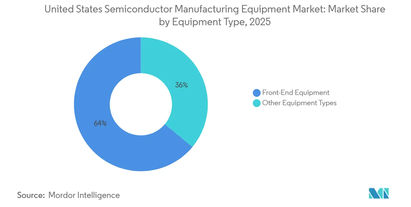
- By equipment type, front-end equipment was the largest category, accounting for 64.0% of the United States semiconductor manufacturing equipment market in 2025. Assembly and packaging equipment is forecast to be the fastest-growing category, expanding at a 15.60% CAGR through 2031, driven by demand for heterogeneous integration and AI-oriented packaging.
- By device type, logic and microcomponents were the largest category, representing 32.0% of the market in 2025. Memory equipment is forecast to grow at a 14.50% CAGR through 2031 as high-bandwidth-memory capacity expands.
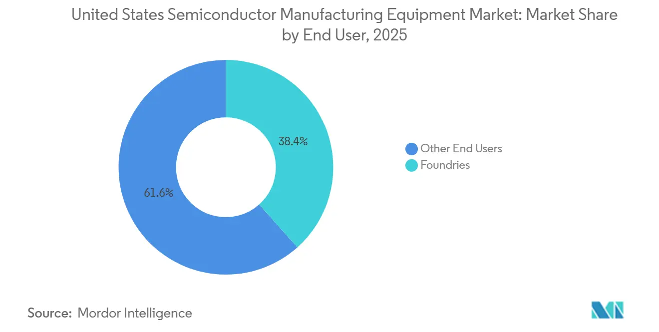
- By end user, foundries were both the largest and fastest-growing category, holding a 38.4% share in 2025 and projected to grow at a 13.40% CAGR through 2031. Growth is led by the United States capacity programs involving TSMC, Samsung, and Intel Foundry.
Note: Market size and forecast figures in this report are generated using Mordor Intelligence’s proprietary estimation framework, updated with the latest available data and insights as of January 2026.
United States Semiconductor Manufacturing Equipment Market Trends and Insights
Drivers Impact Analysis*
| Driver | (~) % Impact on CAGR Forecast | Geographic Relevance | Impact Timeline |
|---|---|---|---|
| CHIPS Act Incentives and Domestic Fab Buildout | +3.5% | National, concentrated in Arizona, Texas, New York, Oregon, and Ohio | Short term (≤ 2 years) to Medium term (2-4 years) |
| AI and High-Performance Computing Capacity Expansion | +2.8% | National, with the highest equipment pull in Arizona and Texas | Short term (≤ 2 years) |
| Advanced-Node Scaling and Greater Equipment Intensity per Wafer | +1.8% | Arizona, Oregon, and Texas | Medium term (2-4 years) |
| Advanced Packaging and Heterogeneous Integration Adoption | +1.2% | Arizona, Texas, and Oregon, expanding to New York and Ohio | Short term (≤ 2 years) to Medium term (2-4 years) |
| Domestic Supply-Chain Resilience and National-Security Procurement | +0.9% | National | Long term (≥ 4 years) |
| High-NA EUV Ecosystem Development in Albany and Other Research Hubs | +0.6% | New York and Oregon | Medium term (2-4 years) to Long term (≥ 4 years) |
| Source: Mordor Intelligence | |||
CHIPS Act Incentives and Domestic Fab Buildout
The CHIPS and Science Act provides USD 39 billion in direct manufacturing incentives and USD 11 billion for research and development infrastructure. By January 2025, 19 companies had received USD 30.7 billion in awards and USD 5.5 billion in loans for 40 commercial fabrication projects. The 35% investment tax credit applies to eligible projects that begin construction before December 31, 2026, thereby supporting earlier equipment ordering. TSMC has committed USD 265 billion for 12 fabrication and packaging facilities in Arizona. Texas Instruments plans to invest more than USD 60 billion across 7 United States fabs in Texas and Utah.
AI and High-Performance Computing Capacity Expansion
AI data centers require more leading-edge logic, higher-bandwidth memory, and greater advanced packaging capacity. The Semiconductor Industry Association projected a 56.3% CAGR for the AI data center ecosystem from 2025 through 2028. SEMI expects global 300mm fab equipment spending to reach USD 142 billion in 2026, rising 25% from the prior year, with logic and memory capacity supporting the increase. Wafer-processing equipment for front-end AI chip production grew 12% in 2025, while test equipment billings increased 55%. Leading-edge logic, DRAM, and advanced packaging accounted for more than 80% of incremental wafer-fab equipment spending in 2026. This concentrates opportunities among suppliers with exposure to those production areas, rather than in demand for mature nodes or legacy equipment.[1]Semiconductor Industry Association, “Powering AI: The Semiconductor Ecosystem at the Foundation of Data Centers,” Semiconductor Industry Association, semiconductors.org.
Advanced-Node Scaling and Equipment Intensity
The United States semiconductor manufacturing equipment market benefits as gate-all-around transistor designs replace FinFET structures at 2nm. Capital expenditure for 50,000 wafers per month of capacity rises from USD 16 billion at 5nm to USD 30 billion at 2nm. Gate-all-around production requires new epitaxial growth, selective etching, and atomic layer deposition processes. TSMC estimates that 2nm wafers require 15%-20% more deposition and etch steps than 3nm wafers. This increases chamber demand, consumable consumption, and process-control requirements. Intel's Hillsboro site operates the first commercial High-NA EUV tool installed in North America. The Albany NanoTech Complex is also installing an ASML TWINSCAN EXE:5200B system, extending High-NA EUV development capacity in New York.
Advanced Packaging, Resilience, and Research Capacity
Advanced packaging is becoming central to equipment selection as chip designers combine logic, memory, and other functions on shared substrates. TSMC plans to increase SoIC capacity from 10,000 to 50,000 wafers per month by 2027. This expansion requires die-attach, wafer-thinning, dicing, and hybrid-bonding equipment. Assembly and packaging equipment billings rose 21% in 2025. United States packaging capacity also supports domestic supply chain resilience and national security procurement requirements. The United States semiconductor manufacturing equipment market is developing a broader local service base as equipment suppliers place engineers, spare parts, and process-support teams closer to new fabs. New York's High-NA EUV program combines USD 1 billion in state funding with USD 9 billion in industry co-funding from companies including Micron, IBM, Applied Materials, and Tokyo Electron.[2]Governor Kathy Hochul, “Governor Hochul Announces World's Most Advanced Equipment for Semiconductor Chip Design Begins Arriving at Albany NanoTech,” New York State, governor.ny.gov.
Restraints Impact Analysis*
| Restraint | (~) % Impact on CAGR Forecast | Geographic Relevance | Impact Timeline |
|---|---|---|---|
| Extreme Capital Intensity and Long Tool Payback Periods | -2.0% | National, most acute in Arizona, Texas, New York, and Oregon | Long term (≥ 4 years) |
| Export Controls and Cross-Border Compliance Complexity | -1.5% | National, with global supply-chain implications | Short term (≤ 2 years) to Medium term (2-4 years) |
| Skilled Field-Service Engineer Shortage | -0.9% | Texas, Arizona, New York, Oregon, Ohio, California, and Idaho | Medium term (2-4 years) |
| Domestic Shortages of Semiconductor-Grade Components and Consumables | -0.5% | National, concentrated in Arizona, Texas, and New York | Medium term (2-4 years) |
| Source: Mordor Intelligence | |||
Extreme Capital Intensity and Long Tool Payback Periods
A leading-edge 2nm fab requires USD 18 billion-USD 25 billion in total capital expenditure, with equipment accounting for 80% of that amount. Mature-node projects still require substantial investment, with a 28nm-65nm fab averaging USD 4.5 billion in capital expenditure. SEMI expects global 300mm fab equipment spending to total USD 374 billion during 2026-2028. Tool payback periods can extend from 5 to 8 years, depending on yields and utilization. The cost of construction and operation in the United States remains higher than in major Asian manufacturing locations. These conditions make financing, incentive terms, skilled service labor, and reliable supplies of specialized components important to equipment purchasing schedules.
Export Controls and Compliance Complexity
Export controls add administrative and commercial constraints for suppliers serving international customers. In December 2024, the Bureau of Industry and Security introduced new controls on advanced-node equipment and high-bandwidth memory, as well as additional foreign-produced direct product rules. The Bureau published further rules in January 2025 covering AI diffusion and due diligence measures for advanced computing integrated circuits. The Government Accountability Office noted that a 25-day review period for Notified Advanced Computing notifications can create scheduling uncertainty for exporters. Companies that previously relied on China-bound equipment shipments must manage licensing, entity list reviews, and third-party due diligence. Smaller suppliers may face greater difficulty absorbing these compliance costs and maintaining the field-service staffing needed across several United States fab regions. The United States semiconductor manufacturing equipment market, therefore, remains exposed to both cross-border compliance requirements and domestic workforce and consumables constraints.[3]United States Government Accountability Office, “Export Controls: Commerce Implemented Advanced Semiconductor Rules and Took Steps to Address Compliance Challenges,” United States Government Accountability Office, gao.gov.
*Our forecasts treat driver/restraint impacts as directional, not additive. The impact forecasts reflect baseline growth, mix effects, and variable interactions.
Segment Analysis
By Equipment Type: Front-End Tools Lead While Packaging Expands
Front-end equipment represented the largest equipment category in the United States semiconductor manufacturing equipment market in 2025, accounting for 64.0% of market revenue. Lithography, deposition, etching, cleaning, chemical mechanical planarization, thermal processing, and metrology are required throughout the wafer production flow. Gate-all-around structures at 2nm require atomic-layer deposition, selective etching, and gate-dielectric steps that older FinFET tool fleets cannot fully support. More process steps per wafer increase demand for chambers, consumables, and inspection touchpoints. ASML is increasing EUV and DUV production capacity by 30% annually during the next 2 years to address customer demand. Applied Materials has stated that deposition and etch are growing faster than lithography at 2nm because the transition raises materials intensity.
Assembly and packaging equipment was the fastest-growing equipment category, supported by heterogeneous integration. Wire-bonding and flip-chip systems continue to support mature-node analog, power, and automotive devices. CoWoS, hybrid bonding, and wafer-level fan-out require more specialized equipment for AI accelerators. TSMC's target of 50,000 SoIC wafers per month by 2027 would require additional die-attach and hybrid-bonding tools. Test equipment billings increased 55% in 2025 as AI chips and stacked high-bandwidth memory required more validation. Factory automation, chemical and gas delivery, and cleanroom systems also benefit from greenfield projects in the United States, where facilities are designed around newer automation architectures. The United States semiconductor manufacturing equipment industry also requires support tools that allow new plants to manage material movement and process utilities from the start.



By Device Type: Logic Leads While Memory Equipment Accelerates
Logic and microcomponents represented the largest device-type category by equipment spending in the United States semiconductor manufacturing equipment market in 2025, with a 32.0% market share. AI accelerators and high-performance processors are directing investment toward advanced logic capacity. TSMC's Arizona program targets leading-edge production technologies for logic customers. Advanced logic requires hundreds of processing steps, multiple EUV patterning passes, and precise back-end interconnect formation. This complexity supports sustained demand for front-end and process-control tools. The United States semiconductor manufacturing equipment market size for advanced logic expands with each new capacity phase, progressing from construction to tool installation.
Memory equipment was the fastest-growing device-type category as HBM3E and HBM4 production scales for AI systems. DRAM equipment sales increased 40.2% in 2024, while NAND equipment sales increased 42.5% in 2025. Micron's Clay fab will need DRAM-focused wafer-fab equipment across several construction and production phases. MPU equipment demand is supported by Intel's 18A and 14A development in Hillsboro. Analog, mixed-signal, discrete, power, sensor, MEMS, and optoelectronic production require tools capable of handling silicon, silicon carbide, and III-V materials.
By End User: Foundries Concentrate High-Value Orders
Foundries represented the largest end-user group in the United States semiconductor manufacturing equipment market in 2025, accounting for 38.4% of market revenue. TSMC, Samsung, and Intel Foundry are focusing on expanding leading-edge fabrication in the United States. Their programs require wafer-fabrication tools and co-located advanced packaging lines. SEMI identifies foundry investment as a major driver of global equipment expansion through 2028. Sub-2nm capacity requires gate-all-around designs and related process technologies. The United States semiconductor manufacturing equipment market share held by foundry demand remains tied to a limited number of large fab programs and their tool move-in schedules.[4]Semiconductor Equipment and Materials International, “300mm Fab Outlook Report,” SEMI, semi.org.
IDMs form the second-largest end-user group, with Intel, Texas Instruments, Micron, and ON Semiconductor maintaining active domestic capital programs. Texas Instruments' planned USD 60 billion investment supports multi-year demand for mature-node deposition, etch, and test tools. OSAT providers primarily need assembly, packaging, and test systems, including equipment for nearshore advanced packaging programs. Amkor's Arizona facility and other United States packaging projects respond to chipmakers' efforts to reduce supply-chain risk. Research and pilot facilities, including the NSTC EUV Accelerator at Albany NanoTech and Intel's Oregon development center, meet the demand for prototype-scale equipment. These smaller orders can be strategically important because they establish process knowledge before high-volume manufacturing purchases begin.
Geography Analysis
The Southwest and Mountain West account for the largest concentration of greenfield advanced-fab investment in the United States semiconductor manufacturing equipment market. Arizona is the most active state for advanced-node construction in 2026, with TSMC's USD 265 billion commitment covering 12 fabrication and packaging facilities in the Phoenix area. Intel also operates high-volume logic and foundry production at its Ocotillo campus in Chandler. Utah hosts 2 of the 7 United States fabs in Texas Instruments' investment plan. This concentration is encouraging equipment suppliers to establish local capacity for engineering, spare parts, and process support. It also makes the regional equipment service network important after initial tool deliveries are completed.
New York is developing as a center for research infrastructure, High-NA EUV work, and future memory production. The NSTC EUV Accelerator at Albany NanoTech has standard-NA EUV capability, while the ASML TWINSCAN EXE:5200B system is in active installation in 2026. The state committed USD 1 billion to the campus, with USD 9 billion in industry co-funding. Micron's Clay project adds a significant potential source of demand for DRAM-oriented equipment. The United States semiconductor manufacturing equipment market size in New York is therefore linked to both research-grade systems and high-volume memory tools. This combination gives the state a role that differs from the largely production-focused clusters in Arizona and Texas.
Oregon, Texas, and Ohio complete the main regional pattern of United States equipment demand. Oregon hosts Intel's Hillsboro campus, including one of fewer than 12 High-NA EUV tools installed globally. Samsung began EUV equipment testing at its Taylor, Texas, site in 2025 as it prepares for 2nm gate-all-around production. Texas also hosts several Texas Instruments fabs and has announced plans for large-scale manufacturing infrastructure. Ohio remains a medium-term source of equipment demand through Intel's phased Columbus-area fab program. The United States semiconductor manufacturing equipment market share across these locations is shaped by the timing of each company’s construction and ramp plans. Geographic dispersion reduces dependence on single-site supply chains and workforces but requires suppliers to maintain a distributed United States field-service structure.
Competitive Landscape
The United States semiconductor manufacturing equipment market has a concentrated top tier of global OEMs and a wider group of specialized suppliers. ASML has a near-monopoly in EUV lithography, while Applied Materials and Lam Research have leading positions in deposition and etch. KLA leads in process control and inspection. Applied Materials, ASML, Lam Research, Tokyo Electron, and KLA account for most front-end equipment spending by value. This structure gives the largest suppliers strong positions in the most critical process steps. It also means that capacity availability at these suppliers can be as important as end-customer demand.
Applied Materials is preparing its USD 5 billion EPIC Center in Silicon Valley for collaborative equipment and process development. Samsung Electronics joined the EPIC Center in February 2026. Applied Materials and TSMC announced a co-innovation partnership in May 2026. Intel's High-NA EUV activity in Oregon and the Albany NanoTech installation also strengthen domestic process-development capabilities. The United States semiconductor manufacturing equipment market gives leading OEMs opportunities to pair tool sales with long-term process development and service agreements.
Competitive openings are most evident in advanced packaging, heterogeneous integration process control, and domestic field-service infrastructure. BE Semiconductor, Kulicke and Soffa, EV Group, ACM Research, and other specialized suppliers can participate in hybrid bonding, panel-level fan-out, and related processes. Teradyne reported USD 1.28 billion in first-quarter fiscal 2026 revenue, up 87% year over year, driven by semiconductor test demand for AI and data-center chips. The United States semiconductor manufacturing equipment market remains concentrated in leading-edge front-end processes, while specialized suppliers address narrower equipment categories. Strong process co-development capability is likely to matter more than price competition in areas such as atomic-layer etch, 3D NAND integration, and hybrid bonding.
United States Semiconductor Manufacturing Equipment Industry Leaders
Applied Materials, Inc.
ASML Holding N.V.
Tokyo Electron Limited
KLA Corporation
SCREEN Holdings Co., Ltd.
Teradyne, Inc.
Advantest Corporation
Hitachi High-Tech Corporation
- *Disclaimer: Major Players sorted in no particular order



United States Semiconductor Manufacturing Equipment Market Report Scope
| Wafer Fab Equipment / Front-End Equipment (lithography, deposition, etching, cleaning, CMP, thermal processing, front-end metrology & inspection equipment, etc.) |
| Assembly and Packaging Equipment (die attach, wire bonding, flip-chip bonding, wafer bumping, thinning, dicing, molding, etc.) |
| Semiconductor Test Equipment (automated test equipment, wafer probers, test handlers, burn-in equipment, and final test equipment) |
| Fab Facility, Automation and Support Equipment (automation systems, wafer handling systems, AMHS, chemical & gas delivery systems, chillers, cleanroom support equipment, etc.)) |
| Logic and Microcomponents (logic ICs, etc.) |
| Memory (DRAM, NAND, HBM, NOR, etc.) |
| Microprocessors (MPUs) |
| Analog (Power management ICs, signal chain, interface Ics, etc.) |
| Discrete and Power Devices (Diodes, transistors, MOSFETs, etc.) |
| Sensors, MEMS and Optoelectronic Devices (Image sensors, MEMS sensors, etc.) |
| Integrated Device Manufacturers (IDMs) |
| Foundries |
| Outsourced Semiconductor Assembly and Test (OSAT) Companies |
| Others (Research & Development (R&D) and Pilot Lines) |
| By Equipment Type | Wafer Fab Equipment / Front-End Equipment (lithography, deposition, etching, cleaning, CMP, thermal processing, front-end metrology & inspection equipment, etc.) |
| Assembly and Packaging Equipment (die attach, wire bonding, flip-chip bonding, wafer bumping, thinning, dicing, molding, etc.) | |
| Semiconductor Test Equipment (automated test equipment, wafer probers, test handlers, burn-in equipment, and final test equipment) | |
| Fab Facility, Automation and Support Equipment (automation systems, wafer handling systems, AMHS, chemical & gas delivery systems, chillers, cleanroom support equipment, etc.)) | |
| By Device Type | Logic and Microcomponents (logic ICs, etc.) |
| Memory (DRAM, NAND, HBM, NOR, etc.) | |
| Microprocessors (MPUs) | |
| Analog (Power management ICs, signal chain, interface Ics, etc.) | |
| Discrete and Power Devices (Diodes, transistors, MOSFETs, etc.) | |
| Sensors, MEMS and Optoelectronic Devices (Image sensors, MEMS sensors, etc.) | |
| By End User | Integrated Device Manufacturers (IDMs) |
| Foundries | |
| Outsourced Semiconductor Assembly and Test (OSAT) Companies | |
| Others (Research & Development (R&D) and Pilot Lines) |


Key Questions Answered in the Report
What is the outlook for United States semiconductor manufacturing equipment through 2031?
The United States semiconductor manufacturing equipment market is forecast to rise from USD 14.4 billion in 2026 to USD 24.8 billion by 2031, at an 11.4% CAGR.
What is driving equipment demand in the United States?
Fab incentives, AI computing capacity, advanced-node production, and advanced packaging are supporting demand for production and support tools.
Which equipment category leads demand in the United States?
Front-end equipment is the largest category because advanced logic manufacturing needs lithography, deposition, etch, and process-control systems.
Which equipment category is growing fastest?
Assembly and packaging equipment is expanding fastest as chipmakers increase hybrid bonding, CoWoS, and other heterogeneous-integration capacity.
Which end users are placing the largest equipment orders?
Foundries are the largest and fastest-growing end-user group, led by capacity programs from TSMC, Samsung, and Intel Foundry.
What are the main constraints on the United States equipment expansion?
High fab costs, lengthy equipment payback periods, export-control compliance, limited field-service talent, and component availability can delay procurement.
Page last updated on:


 Your data is secure and never sold or shared.


