
Semiconductor Back Grinding Wheels Market Size and Share
Market Overview
| Study Period | 2021 - 2031 |
|---|---|
| Market Size (2026) | USD 0.81 Billion |
| Market Size (2031) | USD 1.13 Billion |
| Growth Rate (2026 - 2031) | 7.06 % |
| Fastest Growing Market | Asia-Pacific |
| Largest Market | Asia-Pacific |
| Market Concentration | Medium |
Major Players *Disclaimer: Major Players sorted in no particular order Image © Mordor Intelligence. Reuse requires attribution under CC BY 4.0. | |
Semiconductor Back Grinding Wheels Market Analysis by Mordor Intelligence
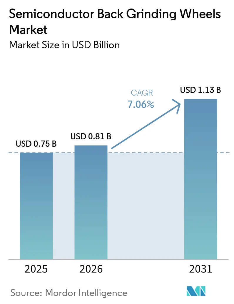
The semiconductor back grinding wheels market size was valued at USD 0.75 billion in 2025 and is estimated to grow from USD 0.81 billion in 2026 to reach USD 1.13 billion by 2031, at a CAGR of 7.06% during the forecast period (2026-2031). The semiconductor back-grinding wheels market is supported by growth in 300 mm wafer production, advanced packaging, and the expansion of silicon carbide (SiC) and gallium nitride (GaN) power-device capacity. These developments increase the number of grinding steps required and the need for precise thickness control on each wafer. Advanced stacking applications are pushing target wafer thicknesses below 50 μm, which increases consumable usage per wafer. Suppliers are responding with specialized bond matrices, fine-grit products, and closer process collaboration with logic, memory, and outsourced semiconductor assembly and test facilities. Supply exposure to synthetic diamond, cobalt, and specialty resins remains a key constraint on the market, as it can affect input availability and supplier margins.
Key Report Takeaways
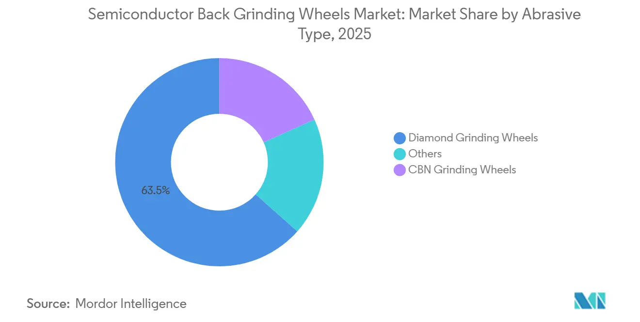
- By abrasive type, diamond grinding wheels held 63.45% of the semiconductor back grinding wheels market share in 2025 and are projected to grow at an 8.06% CAGR through 2031.
- By wafer and substrate material, silicon held 55.33% of the semiconductor back grinding wheels market share in 2025, while silicon carbide (SiC) is forecast to record the highest CAGR of 8.31% through 2031.
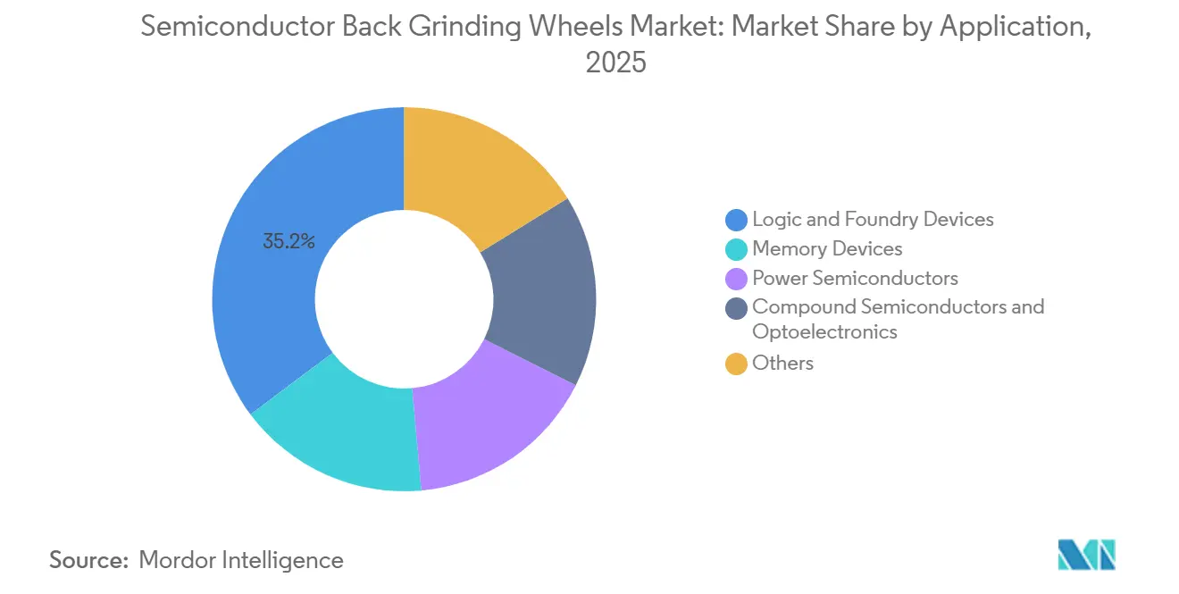
- By application, logic and foundry devices accounted for 35.24% of the semiconductor back grinding wheels market share in 2025, while power semiconductors are projected to expand at an 8.73% CAGR through 2031.
- By geography, Asia-Pacific held 44.76% of the semiconductor back grinding wheels market share in 2025 and is forecast to grow at an 8.42% CAGR through 2031.
Note: Market size and forecast figures in this report are generated using Mordor Intelligence’s proprietary estimation framework, updated with the latest available data and insights as of January 2026.
Market Trends and Insights
Drivers Impact Analysis of Semiconductor Back Grinding Wheels Market*
| Drivers | (~) % Impact on CAGR Forecast | Geographic Relevance | Impact Timeline |
|---|---|---|---|
| Advanced Packaging and Ultra-Thin Wafer Adoption | +2.0% | Global, with core demand in Taiwan, South Korea, and Japan | Short term (≤ 2 years) |
| Expansion of 300 mm Wafer Manufacturing | +1.5% | Global, with the highest incremental spending in Taiwan, China, and North America | Medium term (2-4 years) |
| SiC and GaN Power Semiconductor Scale-Up | +1.6% | Asia-Pacific core, with spillover to Europe and North America | Medium term (2-4 years) |
| HBM, Chiplet, and 2.5D/3D Integration | +1.3% | South Korea and Taiwan, with early gains in Japan and North America | Short term (≤ 2 years) |
| Mainstream Demand for High-Integrity Surface Finishing | +0.8% | Global | Long term (≥ 4 years) |
| In-Line Metrology and Closed-Loop Grinding Optimization | +0.5% | Global, led by fabs at advanced nodes | Long term (≥ 4 years) |
| Source: Mordor Intelligence | |||
Advanced Packaging and Ultra-Thin Wafer Adoption
Advanced packaging has made wafer thinning a yield-critical process rather than a peripheral production step. In HBM3E and HBM4 flows, individual DRAM dies require thicknesses of 30 to 50 μm to meet package-height limits. Stacks with 20 or more layers will require thicknesses well below 30 μm, raising requirements for surface integrity and wheel performance. In February 2026, LINTEC introduced its Pattern Coating Before Lamination process and RAD-3400F/12 resin coater to reduce thickness variation caused by circuit-surface step heights. The process supports consistent performance from higher-grade wheels by reducing thickness variation at wafer entry, thereby reducing defects after back grinding[1]. The semiconductor back-grinding wheels market also benefits as Outsourced Semiconductor Assembly and Test (OSAT) facilities adopt ultra-thin-wafer capabilities for fan-out wafer-level and panel-level packaging.
Expansion of 300 mm Wafer Manufacturing
The expansion of 300 mm manufacturing creates recurring demand for back-grinding consumables throughout a fab's operating life. SEMI expects global 300 mm front-end equipment spending to reach USD 142 billion in 2026, up 25% from 2025. SK Siltron began gradual operations at its 300 mm silicon wafer plant in the Gumi 3 Industrial Complex in July 2026, following a KRW 2.3 trillion investment (~USD 1.7 billion), and has secured customer orders supporting high-90% utilization. GlobalWafers opened its FAB300 facility in Novara, Italy, in October 2025, following a EUR 450 million investment (equivalent to USD 495 million). Migration from 5-inch and 6-inch wafers to 8-inch and 300 mm formats is also spreading across automotive microcontrollers, analog integrated circuits, and sensors, extending demand beyond advanced artificial intelligence devices.
SiC and GaN Power Semiconductor Scale-Up
SiC and GaN substrates are harder and more abrasion-resistant than silicon, requiring specialized bonding chemistry and greater use of grinding wheels per wafer. Mitsubishi Electric began operating a 200 mm SiC power semiconductor processing facility in Kikuchi City in November 2025, following an investment of JPY 100 billion (USD 667 million). The automated line targets a 30% improvement in production efficiency. Bosch reached commercial SiC production in Roseville, California, in 2026 and committed EUR 650 million (USD 715 million) to its Reutlingen SiC facility between 2026 and 2029. In July 2025, Infineon stated that its 300 mm GaN process was progressing toward customer samples and that 300 mm wafers can yield 2.3 times as many chips as established 200 mm wafers. These developments broaden the semiconductor back-grinding wheels market beyond conventional silicon wafer processing.
HBM, Chiplet, and 2.5D/3D Integration
High Bandwidth Memory (HBM) supply lagged demand in 2026, with advanced packaging yield being a more immediate constraint than wafer capacity. HBM4 stacks with more than 16 layers require DRAM wafers with a thickness of 30 μm or less, making total thickness variation important for planarity and interlayer bonding. Chiplet architectures increase the number of separately processed tiles, raising the number of back-grinding events per completed device. SEMI forecasts memory equipment spending to rise 29% in 2026, with demand concentrated among Korean memory fabs and Taiwan-based OSAT partners. These packaging requirements support demand for high-precision wheel specifications in the semiconductor back-grinding wheels market. The same production shift also increases the value of in-line metrology and closed-loop grinding control at advanced nodes.
Restraints Impact Analysis of Semiconductor Back Grinding Wheels Market*
| Restraints | (~) % Impact on CAGR Forecast | Geographic Relevance | Impact Timeline |
|---|---|---|---|
| Semiconductor Capital-Expenditure Cyclicality | -0.5% | Global, pronounced in memory-heavy markets in South Korea and Taiwan | Short term (≤ 2 years) |
| Long Qualification Cycles and Yield-Cost Exposure | -0.4% | Global, with the highest friction at leading-edge fabs | Medium term (2-4 years) |
| Diamond Grit, Cobalt, and Specialty Resin Supply Volatility | -0.3% | Global, with supply risk concentrated in China and the Democratic Republic of the Congo | Short term (≤ 2 years) |
| Substitution by Laser, Plasma Dicing, and Chemical Mechanical Planarization (CMP)-Only Flows | -0.2% | Asia-Pacific advanced-packaging fabs, with early adoption in North America | Long term (≥ 4 years) |
| Source: Mordor Intelligence | |||
Semiconductor Capital-Expenditure Cyclicality
Semiconductor capital spending is cyclical, and grinding-wheel sales can move with fab throughput, as wheels are variable consumables. Memory market volatility is particularly significant because memory fabs account for a large share of wafer-thinning output. SEMI reported sharp changes in NAND equipment spending. This variation can quickly affect fab utilization and reduce near-term demand for semiconductor back grinding wheels. Suppliers serving logic, memory, and power-device customers are better positioned to withstand a correction in any one of these device categories. Long qualification cycles also raise switching costs, as process changes can affect wafer yield and surface quality.
Diamond Grit, Cobalt, and Specialty Resin Supply Volatility
Grinding wheels depend on high-purity diamond grit, cobalt metal powder for metal-bond wheels, and heat-resistant specialty resins. China introduced export licensing requirements, effective November 8, 2025, for synthetic diamond grinding wheels meeting specified technical thresholds. The United States Geological Survey recorded a 30% decline in U.S. imports of industrial diamonds in 2025[2]. Supply tightness can increase input costs and compress margins, particularly for smaller manufacturers without long-term supply agreements. Cobalt exposure compounds this risk, as metal-bond diamond products use cobalt powder, and supply conditions can tighten during demand surges. Over the longer term, alternative processes such as laser dicing, plasma dicing, and chemical mechanical polishing-only flows may also limit certain grinding applications, particularly in advanced packaging.
*Our forecasts treat driver/restraint impacts as directional, not additive. The impact forecasts reflect baseline growth, mix effects, and variable interactions.
Semiconductor Back Grinding Wheels Market Segment Analysis
By Abrasive Type:
Diamond Grinding Wheels Extend Their Lead Through Substrate ComplexityDiamond grinding wheels held 63.45% of the semiconductor back grinding wheels market share in 2025 and are forecast to expand at an 8.06% CAGR through 2031. Their position reflects their ability to process silicon as well as harder, more brittle substrates such as SiC, GaN, and sapphire. Cubic Boron Nitride (CBN) and conventional abrasives cannot provide equivalent removal rates and damage control across the full range of materials entering high-volume production. A peer-reviewed 2024 study assessed five back-grinding wheel specifications across silicon, GaP, SiC, and sapphire. It found that bond modulus selection affected material removal and subsurface damage, with 122.07 GPa identified as the optimum bond modulus for SiC under the tested conditions. This technical requirement supports demand for qualified diamond products in the semiconductor back-grinding wheels market.
Vitrified-bond diamond wheels are gaining importance in ultra-precision fine-grinding stages because their porosity and self-sharpening behavior support consistent processing. Resin-bond diamond wheels remain important for finish-grinding steps where thermal stability requirements are less demanding. CBN wheels occupy a narrower role where contamination from cobalt-bonded diamond matrices is a concern. They may also serve selected compound-semiconductor structures where crystal sensitivity limits abrasive contact forces. Mixed-abrasive and advanced resin-bond formats are being developed for domestic SiC processing in China. These product developments indicate that the semiconductor back grinding wheels industry continues to require distinct wheel specifications for removal rate, thermal control, and surface integrity.

By Wafer and Substrate Material:
Silicon Anchors Output While Wide-Bandgap Substrates Redefine MarginsSilicon held 55.33% of the semiconductor back grinding wheels market share in 2025, supported by the large installed base of 300 mm silicon fabs. The migration of automotive and consumer semiconductor production to 300 mm wafers reinforces this baseline demand. Silicon processing provides stable wheel output, although its growth remains below the overall market rate because standard logic and memory thinning are relatively mature. Wider 300 mm production continues to require recurring grinding-wheel replacement as fabs operate at higher throughput. The semiconductor back grinding wheels market size for silicon remains tied to the installed production base and the ongoing shift toward larger wafer formats. This steady output gives suppliers a foundation for serving higher-value substrate applications.
SiC is forecast to grow at an 8.31% CAGR through 2031, making it the fastest-growing wafer material segment. Its growth is linked to electric-vehicle drivetrain inverters, grid power conversion, and data-center power-supply upgrades. GaAs and GaN remain smaller segments but require specialized product qualification at compound-semiconductor and optoelectronics fabs. Sapphire continues to require dedicated grinding chemistry due to its high hardness, supporting demand for replacement wheels in light-emitting diode (LED) chip production. A 2024 publication identified adjustable vitrified-bond porosity and interfacial wettability with diamond as important factors for ultra-fine SiC and GaN grinding wheels. Suppliers serving these substrates need to meet tight surface-quality requirements.
By Application:
Power Semiconductors Outpace Legacy Segments on Structural DemandLogic and foundry devices represented 35.24% of the semiconductor back grinding wheels market share in 2025, making them the largest application category. Advanced foundry production at TSMC, Samsung, and GlobalFoundries requires wafer thinning before advanced packaging assembly. The global increase in 300 mm capacity supports this application's output position. Logic and foundry processing also benefits from a large base of outsourced semiconductor assembly and test (OSAT) partners that require reliable thickness control. This installed demand helps maintain wheel use across multiple device generations and links the semiconductor back grinding wheels market to growth in advanced-node production and packaging activity.
Power semiconductors are projected to grow at an 8.73% CAGR through 2031, the fastest rate among the application categories. SiC and GaN power devices require tighter control of total thickness variation and higher wheel utilization per wafer than conventional silicon logic. Memory is a cyclical but important category because high-bandwidth memory (HBM) stacks require deeper die thinning than conventional DRAM packages. Compound semiconductors and optoelectronics are expanding with GaN radio-frequency devices, SiC Schottky diodes, solar inverters, and electric-vehicle chargers. The Others category includes microelectromechanical systems, image sensors, and power-management integrated circuits. Their packaging increasingly includes die-thinning steps that were not previously standard, expanding the potential application base.
Geography Analysis
APAC Semiconductor Back Grinding Wheels Market
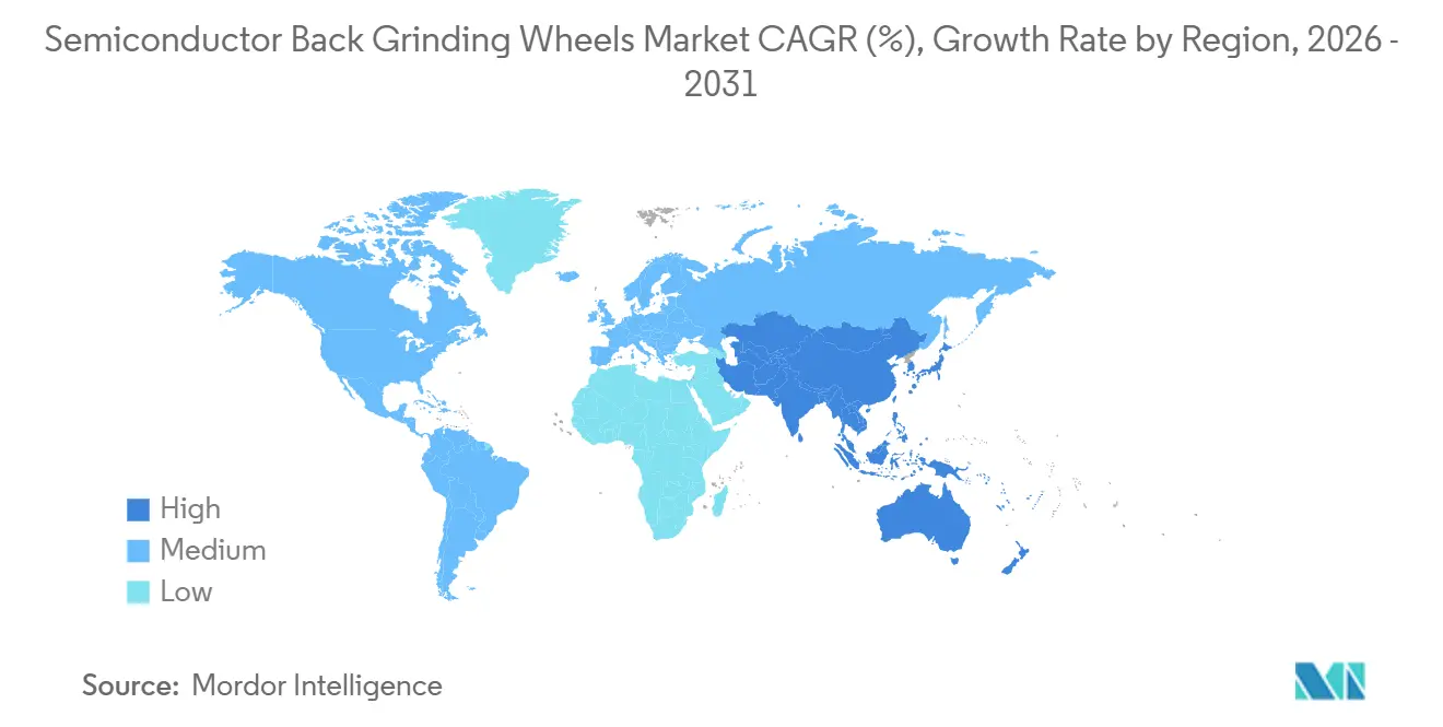
Asia-Pacific held 44.76% of the semiconductor back grinding wheels market share in 2025 and is forecast to grow at an 8.42% CAGR through 2031. The region combines dense wafer fabrication, Outsourced Semiconductor Assembly and Test (OSAT), and grinding wheel manufacturing capacity across Japan, South Korea, Taiwan, and China. Japan remains a major center for wheel development and materials research. South Korean integrated device manufacturers operate high-capacity thinning lines for High Bandwidth Memory (HBM) and NAND production. Taiwan combines TSMC's advanced packaging activity with a broad OSAT network that requires 300 mm back grinding capacity. China is expanding mature-node semiconductor production while developing domestic grinding wheel capabilities.
North America and Europe Semiconductor Back Grinding Wheels Market
North America recorded USD 10.9 billion in semiconductor equipment spending in 2025, supported by fab construction involving Intel, TSMC, Texas Instruments, and other manufacturers. GlobalWafers opened its USD 3.5 billion 300 mm silicon wafer facility in Sherman, Texas, in May 2025. These facilities create a multi-year demand base as production moves toward planned utilization. Europe recorded USD 2.9 billion in semiconductor equipment spending in 2025, a 41% decline from the prior year. European Commission grants totaling EUR 623 million (~USD 724.37 million) for facilities at GlobalFoundries in Dresden and X-FAB in Erfurt support a later recovery in regional wafer production.
South America, APAC and MEA Semiconductor Back Grinding Wheels Market
South America, the Middle East, and Africa account for a smaller share of demand, as activity is concentrated in downstream electronics assembly rather than wafer fabrication. Saudi Arabia's Vision 2030 plans include developing a domestic semiconductor supply chain. India has a USD 15 billion semiconductor incentive program and approvals for ongoing fab construction. These programs establish conditions for future wheel demand later in the forecast period, though their near-term effect remains limited given the time required to build and qualify large-scale wafer fabrication facilities. The semiconductor back grinding wheels market will therefore remain centered on established production regions while newer locations develop supporting capacity.
Competitive Landscape
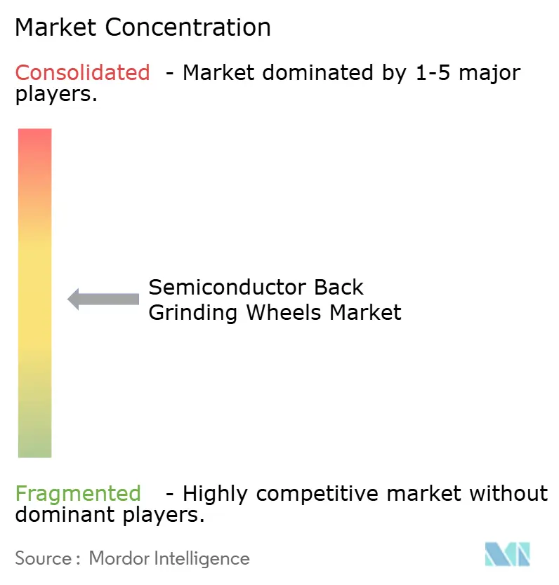
The semiconductor back grinding wheels market is moderately fragmented at the premium tier. DISCO Corporation, Asahi Diamond Industrial, and A.L.M.T. Corp. hold strong positions in advanced-node and wide-bandgap substrate grinding. EHWA Diamond and Shinhan Diamond Ind. Co., Ltd. compete across a broad range of products from South Korea. Competition depends on bond-matrix engineering, product qualification, and collaboration with logic and memory fabs. Suppliers that combine consumables with equipment relationships can influence wheel specifications during machine qualification, making process capability and customer validation as important as product availability.
DISCO launched the DFG8561, a fully automatic grinder with a 6.3 kW spindle developed for difficult-to-grind materials such as SiC and sapphire. Asahi Diamond announced its Medium-Term Management Plan 2030 in May 2026, targeting JPY 53 billion (~USD 0.33 billion) in sales by fiscal year 2030, equivalent to USD 353 million, compared with JPY 42 billion (~USD 0.26 billion) in fiscal year 2025. The company plans to invest JPY 15 billion (~USD 0.09 billion) to JPY 30 billion (~USD 0.18 billion) in growth over five years and has identified electronics and semiconductors as its highest-priority segment. These developments reflect how companies are using equipment development and targeted investment to maintain qualification positions.
Asahi Diamond Industrial and Tokyo Seimitsu began commercial sales of hub blades through AA Diamond Technology in July 2026. The partnership supports consumable cross-qualification where either company has existing equipment relationships. Chinese suppliers are developing ultra-fine-grit SiC and GaN wheel formulations, increasing competitive pressure in applications where Japanese suppliers have held a qualification advantage. SEMI and ISO-related qualification requirements continue to affect supplier selection at leading fabs, as reflected in the inclusion of ISO 9001 certification in AA Diamond Technology's July 2026 hub-blade announcement. The semiconductor back grinding wheels market has a concentration score of 6 out of 10, as a small group of Japanese and South Korean specialists leads the premium tier, though the available information does not establish a combined top-five market share of at least 70%.
Semiconductor Back Grinding Wheels Industry Leaders
-
DISCO CORPORATION
-
Saint-Gobain
-
Asahi Diamond Industrial Co.,Ltd.
-
KINIK COMPANY
-
EHWA DIAMOND
- *Disclaimer: Major Players sorted in no particular order
Semiconductor Back Grinding Wheels Market Companies Covered in this Report
- A.L.M.T. Corp.
- Asahi Diamond Industrial Co.,Ltd.
- DISCO CORPORATION
- EHWA DIAMOND
- KINIK COMPANY
- KURE GRINDING WHEEL
- Nanjing Sanchao Advanced Materials Co., Ltd
- NORITAKE CO., LIMITED
- Saesol Diamond
- Saint-Gobain
- Shinhan Diamond Ind. Co., Ltd.
- Suzhou Sail Science and Technology Co., Ltd.
- TOKYO SEIMITSU CO., LTD
- Tyrolit AG
- UKAM Industrial Superhard Tools
Recent Industry Developments in Semiconductor Back Grinding Wheels Market
- July 2026: Asahi Diamond Industrial Co., Ltd. and Tokyo Seimitsu Co., Ltd. began commercial sales of hub blades through their joint venture, AA Diamond Technology Co., Ltd., targeting semiconductor dicing applications, including generative AI-related devices. The joint venture was established following a Memorandum of Understanding (MOU) signed in January 2025 and has achieved ISO 9001 certification, enabling both companies to cross-qualify consumables at fabs where either holds existing equipment relationships.
- February 2026: LINTEC Corporation announced the Pattern Coating Before Lamination (PCBL) process and the RAD-3400F/12 resin coater to reduce thickness variation during semiconductor wafer back grinding caused by step-height differences on circuit surfaces. Full-scale orders were accepted from April 2026. The process improves back grinding yield for bumped and patterned wafers used in advanced packaging.
Global Semiconductor Back Grinding Wheels Market Report Scope
Semiconductor back grinding wheels are precision diamond abrasive tools used to thin the backside of silicon, silicon carbide, or gallium nitride wafers during the back-end chip manufacturing process. They remove excess bulk material to reduce wafer thickness, often to less than 100 micrometers, enabling chips to fit into compact devices and supporting advanced 3D stacking.
The semiconductor back grinding wheels market is segmented by abrasive type, wafer and substrate material, application, and geography. By abrasive type, the market is segmented into diamond grinding wheels, CBN grinding wheels, and others. By wafer and substrate material, the market is segmented into silicon, silicon carbide (SiC), gallium nitride (GaN), sapphire, gallium arsenide (GaAs), and others. By application, the market is segmented into logic and foundry devices, memory devices, power semiconductors, compound semiconductors and optoelectronics, and others. The report also covers market size and forecasts for the semiconductor back grinding wheels market across 15 countries in major regions. The market sizes and forecasts are provided in terms of value (USD).
Segmentation Overview
| Diamond Grinding Wheels |
| CBN Grinding Wheels |
| Others |
| Silicon |
| Silicon Carbide (SiC) |
| Gallium Nitride (GaN) |
| Sapphire |
| Gallium Arsenide (GaAs) |
| Others |
| Logic and Foundry Devices |
| Memory Devices |
| Power Semiconductors |
| Compound Semiconductors and Optoelectronics |
| Others |
| Asia-Pacific | China |
| India | |
| Japan | |
| South Korea | |
| ASEAN Countries | |
| Rest of Asia-Pacific | |
| North America | United States |
| Canada | |
| Mexico | |
| Europe | Germany |
| United Kingdom | |
| France | |
| Italy | |
| NORDIC Countries | |
| Rest of Europe | |
| South America | Brazil |
| Argentina | |
| Rest of South America | |
| Middle East and Africa | Saudi Arabia |
| South Africa | |
| Rest of Middle East and Africa |
| By Abrasive Type | Diamond Grinding Wheels | |
| CBN Grinding Wheels | ||
| Others | ||
| By Wafer and Substrate Material | Silicon | |
| Silicon Carbide (SiC) | ||
| Gallium Nitride (GaN) | ||
| Sapphire | ||
| Gallium Arsenide (GaAs) | ||
| Others | ||
| By Application | Logic and Foundry Devices | |
| Memory Devices | ||
| Power Semiconductors | ||
| Compound Semiconductors and Optoelectronics | ||
| Others | ||
| By Geography | Asia-Pacific | China |
| India | ||
| Japan | ||
| South Korea | ||
| ASEAN Countries | ||
| Rest of Asia-Pacific | ||
| North America | United States | |
| Canada | ||
| Mexico | ||
| Europe | Germany | |
| United Kingdom | ||
| France | ||
| Italy | ||
| NORDIC Countries | ||
| Rest of Europe | ||
| South America | Brazil | |
| Argentina | ||
| Rest of South America | ||
| Middle East and Africa | Saudi Arabia | |
| South Africa | ||
| Rest of Middle East and Africa | ||
Key Questions Answered in the Report
What is current market size of Semiconductor Back Grinding Wheels Market?
The semiconductor back grinding wheels market size was valued at USD 0.75 billion in 2025 and is estimated to grow from USD 0.81 billion in 2026 to reach USD 1.13 billion by 2031, at a CAGR of 7.06% during the forecast period (2026-2031).
Which abrasive type drives demand for semiconductor back grinding wheels?
Diamond grinding wheels led with a 63.45% share in 2025 and are forecast to grow at an 8.06% CAGR through 2031. Their broad use across silicon, SiC, GaN, and sapphire supports this position.
Why are SiC and GaN important for back grinding wheel suppliers?
SiC and GaN are harder substrates that require specialized wheel formulations, while SiC is projected to expand at an 8.31% CAGR through 2031. Their use in power devices increases the importance of surface control and specialized bond chemistry.
Which application is growing fastest for semiconductor back grinding wheels?
Power semiconductors are forecast to grow at an 8.73% CAGR through 2031 because SiC and GaN devices require precise thinning and higher wheel use per wafer. Logic and foundry devices remain the largest application category.