
Semiconductor Assembly and Packaging Equipment Market Size and Share
Market Overview
| Study Period | 2020 - 2031 |
|---|---|
| Market Size (2026) | USD 10.61 Billion |
| Market Size (2031) | USD 19.68 Billion |
| Growth Rate (2026 - 2031) | 13.15 % |
| Fastest Growing Market | Asia-Pacific |
| Largest Market | Asia-Pacific |
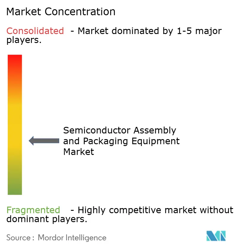
| Market Concentration | Medium |
Major Players *Disclaimer: Major Players sorted in no particular order Image © Mordor Intelligence. Reuse requires attribution under CC BY 4.0. | |
Semiconductor Assembly and Packaging Equipment Market Analysis by Mordor Intelligence
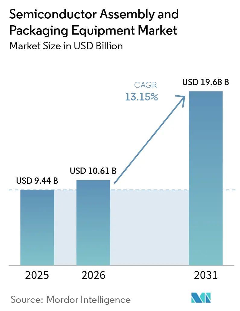
The semiconductor assembly and packaging equipment market was valued at USD 9.44 billion in 2025 and is estimated to grow from USD 10.61 billion in 2026 to reach USD 19.68 billion by 2031, registering a CAGR of 13.15% during the forecast period (2026-2031).
Demand for semiconductor assembly and packaging equipment is being driven by the growing adoption of advanced packaging technologies, particularly for artificial intelligence accelerators, high-bandwidth memory, chiplets, and high-performance computing applications. As semiconductor architectures become increasingly complex, manufacturers are requiring equipment with higher precision, throughput, and process control across die bonding, wafer thinning, dicing, molding, inspection, metrology, and lithography. The increasing integration of multiple dies within a single package is also raising the importance of advanced assembly capabilities and yield optimization.
Asia-Pacific remains the core investment region, supported by its established semiconductor manufacturing and outsourced assembly and test ecosystem across China, Taiwan, South Korea, Japan, and Southeast Asia. However, semiconductor capacity expansion is increasingly broadening to North America, Europe, and India, supported by government incentives, supply-chain diversification initiatives, and strategic investments in domestic semiconductor manufacturing. This geographic expansion, combined with rising demand for advanced packaging, is creating opportunities for equipment suppliers across both mature and next-generation packaging processes.
Key Report Takeaways
- By equipment type, die bonders were the largest category, accounting for 30.55% of the market in 2025, while other packaging equipment is forecast to grow at a 14.60% CAGR through 2031.
- By end user, integrated device manufacturers held the largest share, accounting for 55.30% of the market in 2025, while outsourced semiconductor assembly and test companies are forecast to grow at a 15.20% CAGR through 2031.
- By end-use industry, consumer electronics were the largest segment, accounting for 32.0% of the market in 2025, while medical devices are forecast to grow at a 15.60% CAGR through 2031.
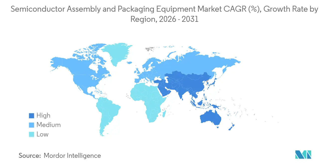
- By geography, Asia-Pacific held the largest market share, accounting for 59.60% in 2025, and is also forecast to be the fastest-growing region, with a 14.15% CAGR through 2031.
Note: Market size and forecast figures in this report are generated using Mordor Intelligence’s proprietary estimation framework, updated with the latest available data and insights as of January 2026.
Market Trends and Insights
Drivers Impact Analysis of Semiconductor Assembly and Packaging Equipment Market*
| Driver | (~) % Impact on CAGR Forecast | Geographic Relevance | Impact Timeline |
|---|---|---|---|
| Advanced Packaging Demand From AI, HPC, and Data Centers | +3.5% | Global, strongest in Asia-Pacific and North America | Short term (≤ 2 years) |
| Chiplet Architectures and Heterogeneous Integration | +2.8% | Global, concentrated in Taiwan, South Korea, and the United States | Medium term (2-4 years) |
| HBM, 2.5D/3D Packaging, and Hybrid Bonding Expansion | +2.4% | Asia-Pacific, with growth in North America | Medium term (2-4 years) |
| Semiconductor Capacity Localization Programs | +1.8% | North America, Europe, Japan, and India | Medium term (2-4 years) |
| Automotive, Power, RF, and Reliability-Critical Package Growth | +1.4% | Europe, North America, and the Asia-Pacific | Medium term (2-4 years) |
| OSAT Outsourcing and Captive Packaging Expansion | +1.0% | Asia-Pacific, with early investment in North America | Short term (≤ 2 years) |
| Source: Mordor Intelligence | |||
Rising Demand for Advanced Packaging in AI, HPC, and Data Center Devices
AI infrastructure spending is increasing demand for advanced semiconductor assembly and packaging equipment across bonding, inspection, and wafer-level processing. Global semiconductor equipment billings reached USD 135.1 billion in 2025, up 15% from 2024, while assembly and packaging equipment billings grew 21%. GPUs, AI accelerators, and HBM stacks require more interconnect density than conventional wire-bond packages can provide. This requirement supports investment in advanced packaging lines for high-performance computing and cloud infrastructure. The semiconductor assembly and packaging equipment market, therefore, benefits from customer programs that involve longer tool qualification periods and more stable production roadmaps. These conditions strengthen the visibility of demand for suppliers already qualified on leading packaging lines.[1]
Shift Toward Chiplet Architectures and Heterogeneous Integration
Chiplet designs require equipment capable of placing and connecting different die types with very fine tolerances. Thermo-compression bonding systems can achieve placement accuracy within 1 µm, which raises their value compared with conventional flip-chip tools. ASMPT secured an order for 8 chip-to-wafer thermo-compression bonding tools from a leading global IDM in June 2026 for chiplet-based client and data-center CPUs. Chiplet integration also adds more interfaces that need to be tested during qualification and yield ramp. This can extend equipment approval cycles from 6 months to 12-18 months. EV Group introduced its LITHOSCALE XT maskless exposure system in 2025 to address the needs of heterogeneous integration, fan-out wafer-level packaging, and AI or HPC patterning.
HBM, 2.5D/3D Packaging, and Hybrid Bonding Capacity Expansion
HBM production is increasing demand for thermo-compression and hybrid bonding equipment. ASMPT received an order in February 2026 for 2 ultrafine-pitch chip-to-wafer thermo-compression bonding tools using its Active Oxide Removal technology. Hybrid bonding requires surface preparation, wafer thinning, plasma activation, bonding, and metrology steps. This raises equipment content per production line compared with traditional bonding methods. BE Semiconductor Industries reported that all 3 major memory manufacturers have their hybrid bonding systems on hold for HBM qualification in 2026. The semiconductor assembly and packaging equipment market is gaining from this broader process flow because a single HBM line needs several specialized systems. The move from qualification to production should also increase recurring demand for related inspection and process-control equipment.
Capacity Localization Fueled by Semiconductor Sovereignty Programs
Government-supported capacity programs are creating new demand for advanced packaging equipment. The United States CHIPS Program Office had finalized or preliminarily agreed to more than USD 34 billion in direct funding by June 2026, including funding for packaging and back-end manufacturing. ESMC plans to install the tool at its Dresden facility in the second half of 2026; the tool is designed to serve automotive, industrial, and IoT applications. Japan is also adding semiconductor capacity through projects linked to TSMC Kumamoto, Kioxia, and Rapidus. SEAJ forecasts fiscal 2026 semiconductor and FPD manufacturing equipment sales of JPY 5.5 trillion, up 12%. These programs make regional packaging capability part of wider semiconductor supply-chain planning. They also create opportunities for suppliers that can provide local service, application support, and compliant component supply.[2]
Restraints Impact Analysis of Semiconductor Assembly and Packaging Equipment Market*
| Restraint | (~) % Impact on CAGR Forecast | Geographic Relevance | Impact Timeline |
|---|---|---|---|
| High Capital Intensity for Advanced Packaging Tooling | -2.5% | Global, with greater pressure on mid-tier OSATs and new entrants | Long term (≥ 4 years) |
| Qualification, Yield Ramp, and Process Integration Complexity | -1.8% | Global, strongest at leading-edge HBM and logic packaging lines | Medium term (2-4 years) |
| Advanced Substrate, Interposer, and Materials Constraints | -1.2% | Global, centered in Asia-Pacific with effects in North America and Europe | Medium term (2-4 years) |
| Export Controls and Precision Component Supply Constraints | -0.8% | Global, with significant effects on China-based tool makers and OSATs | Medium term (2-4 years) |
| Source: Mordor Intelligence | |||
High Capital Intensity for Advanced Packaging Tooling
Advanced packaging lines require substantial spending on bonding, surface preparation, inspection, and cleanroom infrastructure. A CoWoS line expansion of 10,000 wafers per month can require USD 1.5-2.0 billion in capital expenditure. Hybrid bonding and high-end thermo-compression bonding platforms also cost much more than conventional wire-bond systems. Equipment makers must often support customer qualification for 6-18 months before a system generates production revenue. This financial and technical burden limits the number of operators that can move rapidly into leading-edge packaging. The semiconductor assembly and packaging equipment market is therefore split between large foundries, IDMs, and well-funded OSATs that can deploy advanced tools, and smaller firms that remain focused on established package types.
Backend Supply-Chain Exposure to Export Controls and Precision Component Shortages
Export controls can delay the supply of advanced packaging equipment and precision components. In December 2024, the United States Department of Commerce expanded controls on advanced semiconductor manufacturing equipment and added 140 entities to the Entity List. The controls were further reflected in policy guidance covering advanced computing and semiconductor manufacturing items for China. Suppliers need licenses for specified equipment transactions, which can lengthen procurement schedules. Precision bonding heads, laser systems, and alignment modules are especially sensitive because they come from a limited group of qualified suppliers. The resulting uncertainty can affect customer delivery plans and create different competitive conditions across regional markets.[3]
*Our forecasts treat driver/restraint impacts as directional, not additive. The impact forecasts reflect baseline growth, mix effects, and variable interactions.
Semiconductor Assembly and Packaging Equipment Market Segment Analysis
By Equipment Type:
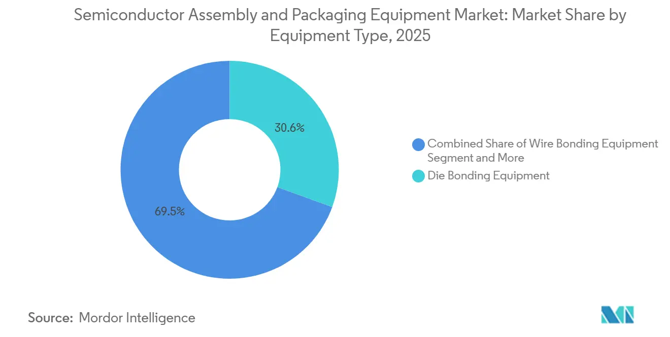
Die Bonding Leads as Advanced Integration DeepensDie bonders held the largest share of the semiconductor assembly and packaging equipment market, accounting for 30.55% in 2025. The segment supports conventional, flip-chip, and advanced packaging processes, including high-bandwidth memory and chiplet-based architectures. Its lead is reinforced by HBM production, which requires accurate die-to-die and die-to-wafer bonding. ASMPT reported USD 339 million in advanced packaging revenue in the first half of 2026, up 17% year over year, with thermo-compression bonding, high-precision SMT, and photonics systems among its main contributors. Wire bonding remains relevant in automotive power modules, RF front ends, LEDs, and other applications that favor established aluminum or copper wire processes. The semiconductor assembly and packaging equipment market size for die bonding is supported by the need to add more interconnect layers as package designs become denser.
Dicing and singulation equipment continues to benefit from the shift toward thinner, more fragile dies in 3D structures. DISCO reported FY2025 net sales of JPY 436.9 billion and an operating income margin of 42.3%, supported by demand for high-value-added products. Inspection and metrology are becoming more important as defects at hybrid-bonding interfaces can reduce yield. KLA expected advanced packaging revenue of USD 1 billion in fiscal 2026, compared with USD 635 million in 2025. In June 2026, Camtek received orders exceeding USD 105 million from a Tier-1 OSAT and a leading HBM manufacturer. Wafer thinning, backgrinding, and surface preparation also become increasingly important because 3D stacking requires wafers to be thinned before bonding.

By Packaging Technology:
Advanced Formats Increase Equipment ContentConventional packaging retained the largest installed base and a significant share of the semiconductor assembly and packaging equipment market in 2025. It continues to support consumer electronics, power devices, and IoT products where wire-bond and leadframe methods remain cost-effective. Flip-chip packaging also retains a substantial revenue role in smartphone processors, networking ASICs, and CPUs. ASMPT’s February 2026 chip-to-wafer platform order showed that ultrafine-pitch bonding is increasingly important for advanced logic applications. Conventional formats are still growing in absolute demand, although a smaller portion of new capital spending is going to these tools.
Wafer-level and fan-out packaging are expanding as wearables, RF modules, and edge AI devices require higher I/O density in thinner packages. STMicroelectronics established a panel-level packaging pilot line in Tours, France, in 2025 for RF, analog, power, and microcontroller devices. The 2.5D and 3D packaging category has the highest equipment spending per unit because it needs multiple bonding, inspection, and thinning steps. Hybrid bonding and DBI are smaller in volume but are expected to grow fastest as HBM and logic-on-logic designs become more common. BE Semiconductor Industries projected hybrid-bonding revenue of EUR 476 million in 2026. System-in-Package tools also serve automotive, industrial IoT, and wearable health applications that combine analog, digital, and RF components.
By End User:
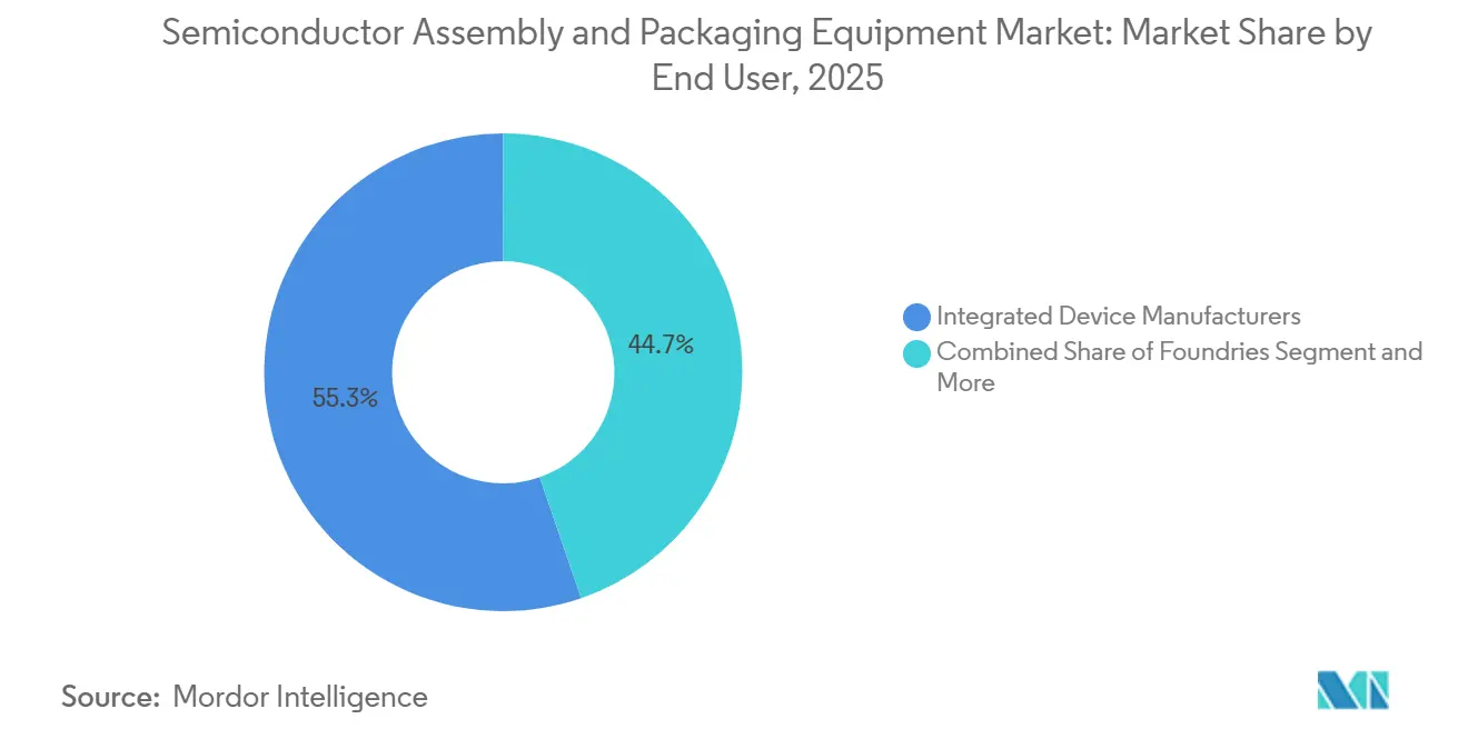
IDMs Anchor Spending While OSATs ExpandIntegrated device manufacturers (IDMs) represented the largest end-user segment, accounting for 55.30% of the market in 2025. This reflects their in-house investments in advanced packaging, hybrid bonding, high-bandwidth memory, and heterogeneous integration. Samsung, SK hynix, Intel, and Micron are investing in equipment for HBM qualification, chiplet integration, and advanced logic packaging. Their purchases tend to focus on high-value hybrid bonders, thermo-compression systems, and 3D metrology platforms. ASMPT’s June 2026 order for 8 chip-to-wafer thermo-compression bonding tools illustrates the scale of IDM demand for advanced CPU packaging. Some IDMs are also sourcing from multiple suppliers to reduce equipment availability risks.
OSATs are the fastest-growing buyer group because more advanced packaging work is being outsourced. ASE increased its 2026 capital expenditure plan to USD 8.5 billion from USD 5.3 billion in 2025 and targeted advanced packaging revenue of USD 3.2 billion in 2026. This expansion supports demand for bonding, inspection, lithography, and test-related systems. Foundries are also becoming important direct customers as they build CoWoS, SoIC, and panel-level packaging capacity. Research institutes and pilot lines have lower spending, but they help validate new hybrid-bonding and wafer-level packaging tools before large-volume customer deployment. The semiconductor assembly and packaging equipment industry benefits from this buyer mix because investments are coming from multiple types of semiconductor producers.
By End-Use Industry:
Computing and AI Define Equipment DemandConsumer electronics was the largest end-use industry, accounting for 32.0% of the market in 2025, driven by sustained demand for smartphones, tablets, wearables, and other connected electronic devices. The shift toward 5G RF modules, under-display sensors, and on-device AI creates demand for fan-out wafer-level packaging and heterogeneous SiP tools. These systems can replace older wire-bond capacity with higher-value equipment. Computing, AI, and data-center applications are the strongest drivers of incremental orders for advanced tools. SEMI identified device complexity and the requirements of AI and HBM semiconductors as key drivers of growth in assembly and packaging equipment in 2025.
Automotive electronics provides a stable demand base because vehicle platforms have qualification cycles of 5-7 years. EV power modules and SiC or GaN devices require specialized sintering and high-temperature bonding methods. Telecommunications, aerospace and defense, and industrial electronics diversify demand beyond AI infrastructure. Medical devices are the fastest-growing end-use vertical because implantable devices, biosensors, and hearing processors require small packages with high reliability. These applications need hermetic sealing, thin packages, and die-level traceability. This supports premium equipment spending and extensive inspection requirements.
Geography Analysis
APAC Semiconductor Assembly and Packaging Equipment Market
Asia-Pacific held the largest share of the semiconductor assembly and packaging equipment market, accounting for 59.60% in 2025, and is projected to remain the fastest-growing region, at a 14.15% CAGR through 2031. Taiwan’s total semiconductor equipment spending rose 90% to USD 31.5 billion in 2025 as TSMC increased CoWoS, SoIC, and co-packaged optics capacity. South Korea’s spending rose by 26% to USD 25.8 billion, supported by investments in HBM production. China spent USD 49.3 billion on semiconductor equipment in 2025, although controls are directing some purchases toward domestic alternatives. Japan’s equipment sales increased 22% to USD 9.5 billion in 2025. Malaysia, Vietnam, Singapore, the Philippines, and Thailand are also attracting OSAT capacity, which broadens regional equipment demand.
North America and India Semiconductor Assembly and Packaging Equipment Market
North America is expanding its advanced packaging base through public support and new investments by companies. The United States CHIPS Program Office had agreed, or had preliminarily agreed, to more than USD 34 billion in direct funding by June 2026. Amkor broke ground on its USD 7 billion packaging and test campus in Peoria, Arizona, in October 2025. The company acquired an additional 67-acre parcel near the campus in May 2026. North American semiconductor equipment spending declined by 20% to USD 10.9 billion in 2025, reflecting slower growth following earlier expansion. India is at an earlier stage, with packaging activity centered on mid-range devices and power applications.[4]
EMEA and South America Semiconductor Assembly and Packaging Equipment Market
Europe recorded USD 2.9 billion in semiconductor equipment spending in 2025, down 41% as automotive and industrial demand weakened. ESMC is preparing its Dresden fab for tool installation in the second half of 2026 and targets first wafer production in late 2027. The facility will serve automotive, IoT, and industrial markets. STMicroelectronics is also developing a panel-level packaging pilot line in France. The Netherlands remains important because of Besi’s advanced position in the bonding equipment sector. South America, the Middle East, and Africa have limited direct demand for equipment, but Israel contributes to the global supply chain through manufacturing inspection equipment.
Competitive Landscape
The semiconductor assembly and packaging equipment market is moderately concentrated in specific tool categories but remains fragmented overall. ASMPT and BE Semiconductor Industries hold strong positions in thermo-compression and hybrid bonding. ASMPT reported record advanced packaging revenue of USD 339 million in the first half of 2026. It also secured orders for more than 50 chip-to-substrate thermo-compression bonding tools from OSAT customers in July 2026. BESI has hybrid-bonding systems under qualification at all 3 major memory manufacturers. Competition is based on placement accuracy, yield results, customer qualification status, local service, and process integration.
Inspection and metrology are becoming more competitive as advanced packages need tighter defect control. KLA is expanding its advanced packaging process-control business and expects USD 1 billion in related revenue in fiscal 2026. Camtek received more than USD 105 million in multi-system orders in June 2026 and acquired Visual Layer to add AI-supported defect detection capabilities. Onto Innovation launched the Dragonfly G5 inspection system in March 2026 for advanced packaging applications. DISCO remains a leading supplier of dicing and wafer-backgrinding equipment. Its FY2025 results show the commercial value of strong positions in established processing niches.
Panel-level packaging is a developing area where supplier positions are less established. Silicon Box reported shipping 100 million units from its Singapore panel-level packaging factory in October 2025. EV Group’s LITHOSCALE XT and STMicroelectronics Tours pilot line show that large-panel lithography and process tools are moving toward production use. Partnerships are also reshaping the competitive landscape, with Applied Materials and Besi developing the Kinex die-to-wafer hybrid-bonding system. Export-control compliance and secure component supply can influence which suppliers can serve specific customers.
Semiconductor Assembly and Packaging Equipment Industry Leaders
-
ASMPT
-
BE Semiconductor Industries N.V.
-
Kulicke and Soffa Industries, Inc.
-
DISCO Corporation
-
Tokyo Seimitsu Co., Ltd.
-
TOWA Corporation
-
Shinkawa Ltd.
- *Disclaimer: Major Players sorted in no particular order
Semiconductor Assembly and Packaging Equipment Market Companies Covered in this Report
- ASMPT
- BE Semiconductor Industries N.V.
- Kulicke and Soffa Industries, Inc.
- DISCO Corporation
- Tokyo Seimitsu Co., Ltd. / ACCRETECH
- TOWA Corporation
- Shinkawa Ltd.
- Hanmi Semiconductor Co., Ltd.
- SUSS MicroTec SE
- EV Group
- Shibaura Mechatronics Corporation
- Yamaha Robotics / APIC Yamada
- Applied Materials, Inc.
- Tokyo Electron Limited
- SCREEN Holdings Co., Ltd.
- KLA Corporation
- Onto Innovation Inc.
- Camtek Ltd.
- ClassOne Technology
- Veeco Instruments Inc.
- Amtech Systems, Inc.
- Nordson Corporation
Recent Industry Developments in Semiconductor Assembly and Packaging Equipment Market
- July 2026: ASMPT secured bulk orders for more than 50 Chip-to-Substrate (C2S) TCB tools from OSAT customers for cutting-edge AI computing chips, expanding its sole-sourced status across multiple OSAT programs for next-generation AI accelerator assembly; shipments of the 50 tools are expected in the first half of 2027.
- June 2026: Camtek received over USD 105 million in multi-system orders from a Tier-1 OSAT and a leading HBM manufacturer for its advanced packaging inspection and metrology platforms, representing one of its largest single-quarter order events and confirming process-control investment at leading memory and OSAT fabs.
- May 2026: Amkor Technology acquired an additional 67-acre parcel adjacent to its existing 104-acre Peoria, Arizona campus to support future expansion of its planned first United States high-volume OSAT advanced packaging and test facility.
- March 2026: Onto Innovation launched the Dragonfly G5 inspection system and secured qualification at a leading HBM manufacturer, with double-digit unit orders committed for both Dragonfly G5 and 3Di technology.
Global Semiconductor Assembly and Packaging Equipment Market Report Scope
| Die Bonding Equipment |
| Wire Bonding Equipment |
| Flip-Chip and Thermo-Compression Bonding Equipment |
| Wafer Bumping and Plating Equipment |
| Dicing and Singulation Equipment |
| Molding and Encapsulation Equipment |
| Wafer Thinning, Backgrinding and Surface Preparation Equipment |
| Inspection and Metrology Equipment |
| Other Assembly and Packaging Equipment |
| Conventional Packaging |
| Flip-Chip Packaging |
| Wafer-Level Packaging |
| Fan-Out Packaging |
| 2.5D/3D Packaging |
| System-in-Package and Module Packaging |
| Hybrid Bonding / Direct Bond Interconnect |
| Outsourced Semiconductor Assembly and Test Companies |
| Integrated Device Manufacturers |
| Foundries |
| Research Institutes, Pilot Lines and Others |
| Computing, AI and Data Centers |
| Consumer Electronics |
| Automotive Electronics |
| Telecommunications and Networking |
| Industrial Electronics |
| Aerospace and Defense |
| Medical Devices |
| Other End-use Industries |
| North America | United States |
| Canada | |
| Mexico | |
| South America | Brazil |
| Rest of South America | |
| Europe | Germany |
| France | |
| Ireland | |
| Italy | |
| Netherlands | |
| Rest of Europe | |
| Asia-Pacific | China |
| Taiwan | |
| South Korea | |
| Japan | |
| Singapore | |
| Malaysia | |
| Philippines | |
| Vietnam | |
| India | |
| Rest of Asia-Pacific | |
| Middle East and Africa |
| By Equipment Type | Die Bonding Equipment | |
| Wire Bonding Equipment | ||
| Flip-Chip and Thermo-Compression Bonding Equipment | ||
| Wafer Bumping and Plating Equipment | ||
| Dicing and Singulation Equipment | ||
| Molding and Encapsulation Equipment | ||
| Wafer Thinning, Backgrinding and Surface Preparation Equipment | ||
| Inspection and Metrology Equipment | ||
| Other Assembly and Packaging Equipment | ||
| By Packaging Technology | Conventional Packaging | |
| Flip-Chip Packaging | ||
| Wafer-Level Packaging | ||
| Fan-Out Packaging | ||
| 2.5D/3D Packaging | ||
| System-in-Package and Module Packaging | ||
| Hybrid Bonding / Direct Bond Interconnect | ||
| By End User | Outsourced Semiconductor Assembly and Test Companies | |
| Integrated Device Manufacturers | ||
| Foundries | ||
| Research Institutes, Pilot Lines and Others | ||
| By End-use Industry | Computing, AI and Data Centers | |
| Consumer Electronics | ||
| Automotive Electronics | ||
| Telecommunications and Networking | ||
| Industrial Electronics | ||
| Aerospace and Defense | ||
| Medical Devices | ||
| Other End-use Industries | ||
| By Geography | North America | United States |
| Canada | ||
| Mexico | ||
| South America | Brazil | |
| Rest of South America | ||
| Europe | Germany | |
| France | ||
| Ireland | ||
| Italy | ||
| Netherlands | ||
| Rest of Europe | ||
| Asia-Pacific | China | |
| Taiwan | ||
| South Korea | ||
| Japan | ||
| Singapore | ||
| Malaysia | ||
| Philippines | ||
| Vietnam | ||
| India | ||
| Rest of Asia-Pacific | ||
| Middle East and Africa | ||
Key Questions Answered in the Report
What is the projected growth rate through 2031?
The sector is projected to grow at a 13.1% CAGR from 2026 to 2031, reaching USD 19.7 billion by 2031.
Which equipment type leads demand?
Die bonding leads because it supports conventional assembly, flip-chip packaging, and thermo-compression bonding for advanced packages.
Why are hybrid-bonding tools important?
Hybrid bonding supports dense HBM and logic packages, but it also requires tightly controlled preparation, bonding, and metrology steps.
Which region has the strongest equipment demand?
Asia-Pacific leads, supported by investment in Taiwan, South Korea, China, Japan, and Southeast Asia.
What limits the adoption of advanced packaging equipment?
High capital requirements, lengthy qualification cycles, export controls, and constrained precision components can slow equipment deployment.
What is driving semiconductor assembly and packaging equipment demand?
AI accelerators, HBM, chiplets, and 2.5D or 3D packages are increasing the demand for bonding, inspection, thinning, and lithography tools.