
Semiconductor Advanced Packaging Materials Market Size and Share
Market Overview
| Study Period | 2021 - 2031 |
|---|---|
| Market Size (2026) | USD 20.11 Billion |
| Market Size (2031) | USD 31.03 Billion |
| Growth Rate (2026 - 2031) | 9.06 % |
| Fastest Growing Market | Asia-Pacific |
| Largest Market | Asia-Pacific |
| Market Concentration | Medium |
Major Players *Disclaimer: Major Players sorted in no particular order Image © Mordor Intelligence. Reuse requires attribution under CC BY 4.0. | |
Semiconductor Advanced Packaging Materials Market Analysis by Mordor Intelligence
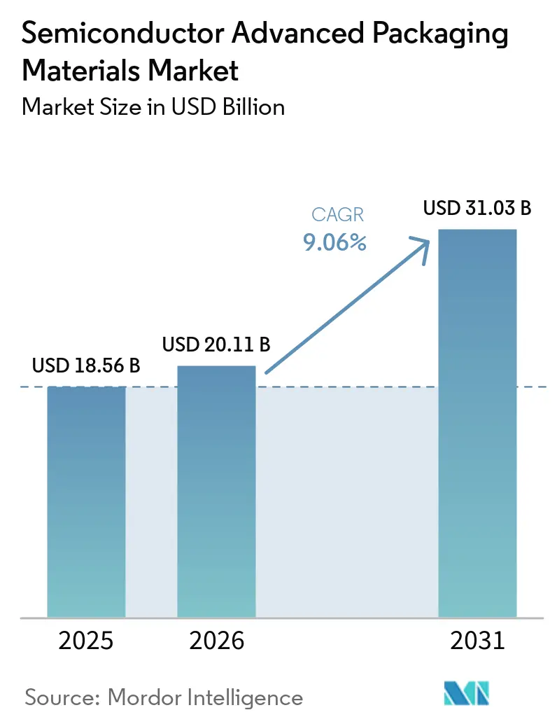
The semiconductor advanced packaging materials market size is valued at USD 18.56 billion in 2025 and is estimated to grow from USD 20.11 billion in 2026 to USD 31.03 billion by 2031, at a CAGR of 9.06% during the forecast period (2026-2031). The semiconductor advanced packaging materials market is expanding as transistor scaling alone no longer delivers the required performance gains. AI accelerators, high-bandwidth memory stacks, and multi-chiplet designs are increasing demand for films, underfills, encapsulants, and thermal materials. Foundries and outsourced semiconductor assembly and test providers are prioritizing materials that have passed process qualifications. This shift moves competition from bulk capacity to collaborative material development and faster product validation. Supply commitments for specialized inputs can limit production expansion, even when packaging capacity is available.
Key Report Takeaways
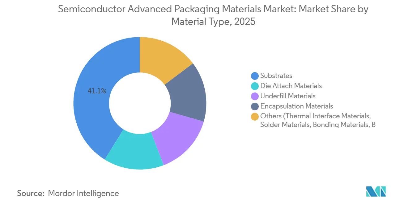
- By material type, substrates held 41.12% of the semiconductor advanced packaging materials market share in 2025, while die attach materials are forecast to grow at a CAGR of 9.53% through 2031.
- By packaging technology, flip-chip held 36.67% of the semiconductor advanced packaging materials market share in 2025, while 2.5D and 3D Integrated Circuit (IC) packaging are forecast to grow at a CAGR of 11.04% through 2031.
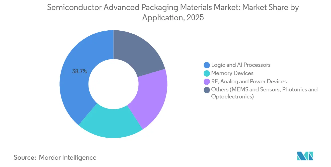
- By application, logic and AI processors held 38.74% of the semiconductor advanced packaging materials market share in 2025 and are forecast to grow at a CAGR of 10.59% through 2031.
- By geography, Asia-Pacific held 39.18% of the semiconductor advanced packaging materials market share in 2025 and is forecast to grow at a CAGR of 9.88% through 2031.
Note: Market size and forecast figures in this report are generated using Mordor Intelligence’s proprietary estimation framework, updated with the latest available data and insights as of January 2026.
Market Trends and Insights
Drivers Impact Analysis of Semiconductor Advanced Packaging Materials Market*
| Drivers | (~) % Impact on CAGR Forecast | Geographic Relevance | Impact Timeline |
|---|---|---|---|
| AI and HBM Package Complexity Increasing Materials Content | +2.8% | Global, with early gains in Taiwan, South Korea, and the U.S. hyperscale supply chains | Short term (≤ 2 years) |
| Heterogeneous Integration and Chiplet Adoption | +1.8% | Global, strongest in Asia-Pacific and North America | Medium term (2-4 years) |
| Miniaturization, Higher I/O Density, and Faster Signal Transmission | +1.0% | Global, especially Japan and Taiwan | Medium term (2-4 years) |
| Automotive Electrification and Advanced Driver-Assistance Systems (ADAS) Reliability Requirements | +0.9% | Europe, Japan, South Korea, and the United States | Medium term (2-4 years) |
| Ajinomoto Build-up Film (ABF) and Low-Loss Material Qualification for Large AI Packages | +1.4% | Global, with supply concentrated in Japan | Short term (≤ 2 years) |
| Thermal Interface Material (TIM) 1.5 and Package-Level Thermal Innovation | +0.7% | Global, with innovation in Japan and the United States | Medium term (2-4 years) |
| Source: Mordor Intelligence | |||
AI and HBM Package Complexity Driving Materials Bill-of-Materials Expansion
Each HBM generation increases the material content required in an AI package. HBM4 entered production in 2026 and requires molded underfill formulations with higher thermal conductivity near the die-to-die physical interface. SK hynix introduced its iHBM thermal solution on May 26, 2026, integrating silicon-based cooling elements into the HBM package. The company stated that the solution reduces thermal resistance by 30% while maintaining compatibility with its Advanced Mass Reflow Molded Underfill (MR-MUF) process. Samsung’s hybrid copper bonding route and SK hynix’s MR-MUF approach create separate qualification paths for underfill materials. Suppliers that align early with a customer’s selected bonding route can secure qualified status, while suppliers serving multiple routes face additional development requirements.
Heterogeneous Integration and Chiplet Adoption Multiplying Interface Layers
Chiplet architectures add die-to-die and die-to-interposer interfaces that require underfill, adhesive, and dielectric treatment. This increases the material requirement for each package rather than simply increasing unit shipments. Intel’s 2025 patent filings described chiplet metallization directly bonded to host integrated circuit (IC) back-end-of-line layers, which could reduce the role of silicon interposers and increase the role of organic redistribution-layer dielectric materials. Therefore, the semiconductor advanced packaging materials market is affected when package designs use more interfaces and more material types. Heterogeneous integration and hybrid bonding remain central technology paths for chiplet development. Foundry-approved material lists can become a practical requirement for participation in specialized packaging programs.
ABF and Low-Loss Material Qualification Creating Structural Supply Constraints
Ajinomoto Build-up Film (ABF) qualification for large AI packages is becoming a supply chain constraint. Ajinomoto announced in May 2026 that it had acquired a new plant site in Kani City, Gifu Prefecture, to expand its buildup film production. The new facility is not scheduled to begin operations until 2032, making the timing of capacity important for substrate producers. Large AI packages also require low-loss materials that support high-frequency signal transmission. These requirements limit the benefit of investing in substrate factories without parallel expansion in upstream inputs. As a result, qualification timing and the availability of physical materials affect the advanced packaging materials market for semiconductors.
TIM1.5 and Package-Level Thermal Innovation Emerging as a Distinct Market Segment
TIM1.5 is applied between a completed package and its cold plate or heat sink during board-level assembly. It has formulation and qualification requirements that differ from those of conventional TIM1 materials. High-performance packages combine High Bandwidth Memory (HBM) stacks, multi-chip modules, and 2.5D structures with materials that respond differently to heat and mechanical stress. This increases the thermomechanical demands on the thermal interface layer[1]. Thermal formulation specialists can participate in this category with fewer front-end process restrictions than suppliers of some other advanced packaging materials. However, the opportunity depends on reliability testing and customer approval.
Restraints Impact Analysis of Semiconductor Advanced Packaging Materials Market*
| Restraints | (~) % Impact on CAGR Forecast | Geographic Relevance | Impact Timeline |
|---|---|---|---|
| High Material Qualification Costs and Long Customer Approval Cycles | -1.5% | Global, with the most severe in North America and Japan | Medium term (2-4 years) |
| Capital Intensity and Yield Sensitivity in Advanced Packaging | -1.2% | Global, especially Taiwan and South Korea | Long term (≥ 4 years) |
| Warpage and Coefficient-of-Thermal-Expansion Mismatch in Large Packages | -0.8% | Global, especially Taiwan, Japan, and South Korea | Medium term (2-4 years) |
| PFAS Substitution and Chemical Traceability Risk | -0.7% | Europe, the United States, and the Asia-Pacific | Long term (≥ 4 years) |
| Source: Mordor Intelligence | |||
High Material Qualification Costs Constraining New Material Adoption Velocity
New materials often require an 18- to 24-month customer qualification cycle. Testing typically covers thermal cycling, moisture sensitivity, mechanical reliability, and, in many cases, wafer-level process integration. A completed qualification for one packaging node may not apply to the next generation if package geometry, layer count, or bonding architecture changes. This requirement strengthens the position of existing approved suppliers in the semiconductor advanced packaging materials market. Long-term supply agreements and capacity reservations for approved materials further support this position. Suppliers outside approved vendor lists for 2.5D and 3D packaging may have limited opportunities to enter the market before the next package generation.
PFAS Substitution and Chemical Traceability: Introducing Multi-Year Compliance Costs
Per- and polyfluoroalkyl substances (PFAS) are used in photoresists, dielectric polymer films, and fluoropolymer thermal management compounds. Replacing them remains technically challenging because alternatives must meet semiconductor performance requirements. The European Chemicals Agency published an updated PFAS restriction proposal under EU REACH in 2025, covering electronics and semiconductor applications, with time-limited derogations under discussion[2]. The National Academy of Engineering identified the need for non-PFAS materials that meet required performance standards and noted that validation can take a decade for demanding semiconductor uses. Multilayer substrates face a specific traceability challenge because fluoropolymer dielectrics may constitute a small mass fraction yet remain essential to high-frequency performance. SEMI has called for risk-based PFAS restrictions, as broad limits could disrupt chip production before alternatives are qualified.
*Our forecasts treat driver/restraint impacts as directional, not additive. The impact forecasts reflect baseline growth, mix effects, and variable interactions.
Semiconductor Advanced Packaging Materials Market Segment Analysis
By Material Type:
Substrates Lead While Die Attach Materials Grow FastestSubstrates accounted for 41.12% of the semiconductor advanced packaging materials market share in 2025. Their position reflected the structural and electrical routing role they play across advanced package types. ABF build-up film, copper-clad laminates, and solder resist form the core substrate material set. Larger AI server packages require more substrate area per unit, while higher layer counts increase build-up film consumption. The IEEE Electronics Packaging Society states that leading redistribution-layer implementations now use 2 µm linewidths, while target dielectric constants are moving toward 2.0 or below. These requirements support the use of low-loss dielectric materials as demand for package signals increases.
Die attach materials are expected to register a 9.53% CAGR from 2026 to 2031, the highest growth rate within this material grouping. Sintered silver die attach films are gaining use in power electronics and dense flip-chip applications, where conventional polymer pastes cannot meet thermal and reliability requirements. Underfill demand is rising with the deeper adoption of flip-chip technology in AI and high-performance computing packages. Large-body flip-chip BGA configurations also require materials that can manage low-gap-height die connections. Encapsulation materials support high-volume mobile and IoT assembly, while thermal interface materials, solder materials, and build-up films are becoming more important. The semiconductor advanced packaging materials industry relies on all these categories to balance heat removal, mechanical reliability, and electrical performance.

By Packaging Technology:
Flip-Chip Accounted for the Largest Share, While 2.5D and 3D IC Packaging Registers the Highest CAGRFlip-chip packaging accounted for 36.67% of the semiconductor advanced packaging materials market share in 2025. It remains widely used for high-pin-count devices, including AI accelerators, network processors, and mobile application processors. A sub-80 µm solder-bump pitch has become standard for these applications. Copper pillar bumping compounds, no-flow underfill films, and large-area encapsulants support the flip-chip materials system. This established system continues to evolve as package sizes increase. Flip-chip also remains a first-level interconnect in some larger multi-die modules. Fan-out packaging is playing a growing role in RF front-end and mobile application processor applications, with reported bill-of-materials savings for 5G RF front ends.
The 2.5D and 3D IC packaging segment is expected to expand at an 11.04% CAGR from 2026 to 2031, making it the fastest-growing packaging technology in the semiconductor advanced packaging materials market. Interposer and organic substrate materials for 2.5D integration require a low coefficient of thermal expansion mismatch, controlled dielectric properties, and compatibility with through-silicon-via processing. These requirements position the segment as a key materials opportunity. Hybrid bonding can reduce reliance on traditional solder bumps and increase demand for copper surface preparation and dielectric polishing materials. Embedded-die and silicon bridge designs create similar material development needs. As a result, the semiconductor advanced packaging materials industry is moving toward material systems designed for denser interconnect structures.
By Application:
Logic and AI Processors Lead Both Share and GrowthLogic and AI processors accounted for 38.74% of the semiconductor advanced packaging materials market in 2025. The segment is also forecast to grow at a 10.59% CAGR from 2026 to 2031. AI inference and training systems are increasing material demand per package. GPUs and ASICs require more underfill, molded encapsulant, and thermal interface treatment as memory capacity per system increases. JEDEC’s 2026 SPHBM4 standard supports HBM4-class bandwidth on organic substrates, broadening memory-logic integration beyond silicon interposers. This development increases the potential role of organic packaging materials in memory-related designs.
Memory devices form the second-largest application category. DRAM and NAND die stacking increase demand for molded underfill films and non-conductive films. The different HBM approaches used by SK hynix and Samsung create parallel qualification paths for underfill and encapsulant suppliers. RF, analog, and power devices remain a stable group that requires ceramic-substrate die attach materials and high-temperature encapsulants. These materials must tolerate demanding operating environments, including continuous temperatures of up to 200°C in certain applications. MEMS, sensors, photonics, and optoelectronics are also gaining attention as co-packaged optics continues to develop. These applications require transparent polymer encapsulants and precision underfill formulations for photonic chiplets.
Geography Analysis
APAC Semiconductor Advanced Packaging Materials Market
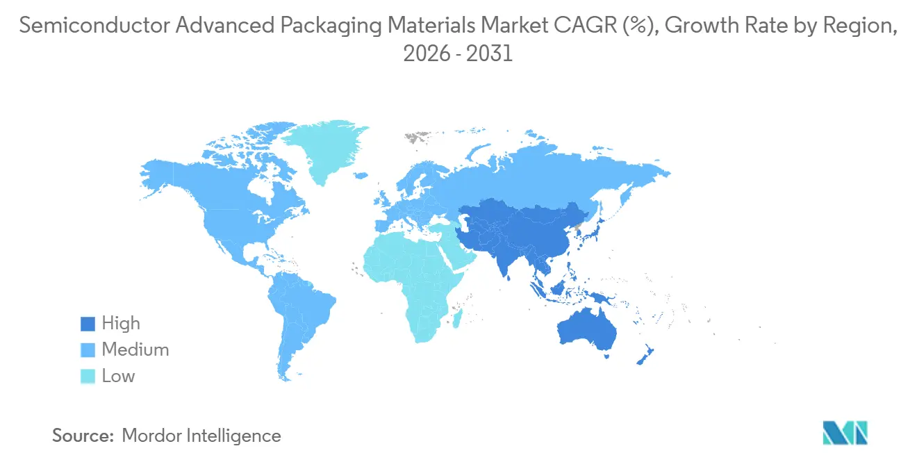
Asia-Pacific held 39.18% of the semiconductor advanced packaging materials market share in 2025 and is forecast to grow at a CAGR of 9.88% through 2031. The region has a high concentration of advanced packaging capacity and semiconductor materials production. Taiwan remains a key hub for IC substrate production. Japan supplies Ajinomoto Build-up Film (ABF), encapsulants, and advanced dielectric polymers to global supply chains. South Korea maintains strong activity in package substrates, supported by demand for AI accelerators and server CPUs. India is emerging as a secondary location for materials applications and innovation centers that support national assembly and packaging plans.
North America and Europe Semiconductor Advanced Packaging Materials Market
North America has the largest concentration of AI chip design activity, but its production assets remain limited relative to design demand. This gap keeps the region dependent on imported advanced packaging materials. Europe is led by Austria’s AT&S, which opened Europe’s first IC substrate production facility in Leoben in June 2025. The project included an investment exceeding EUR 500 million, which the source reported as USD 550 million. Germany has substantial materials supplier activity through Henkel’s portfolio of underfills, encapsulants, and thermal management materials. These capabilities position Europe in substrate manufacturing and specialty materials development.
MEA and South America Semiconductor Advanced Packaging Materials Market
South America, the Middle East, and Africa remained minor contributors to the advanced packaging materials market for semiconductors in 2025. Mexico is attracting electronics manufacturing investment, which could create local demand for encapsulants and adhesives, particularly in automotive and consumer electronics assembly. Middle Eastern countries are investing in semiconductor supply chain infrastructure through national technology programs, although advanced packaging materials capacity in the region remains limited. South Africa and other African locations remain focused on downstream electronics assembly rather than semiconductor packaging. Their future contribution depends on the broader regionalization of the semiconductor supply chain through the late 2020s.
Competitive Landscape
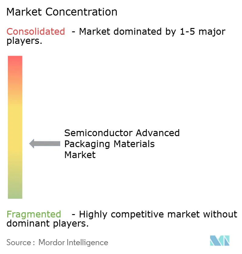
The semiconductor advanced packaging materials market is moderately fragmented. Japanese suppliers set specifications across dielectric films, molded underfill, non-conductive film, and epoxy molding compounds. Foundries, hyperscalers, and outsourced semiconductor assembly and test providers increasingly use co-development agreements to select material partners early. Resonac opened its US-JOINT R&D center in Silicon Valley on April 20, 2026, with 12 member companies, including NAMICS and AMD. The consortium aims to reduce concept validation timelines from six months to one month, providing members with a faster path from material development to customer evaluation.
Opportunities include glass core substrates, panel-level organic interposers, and per- and polyfluoroalkyl substances (PFAS)-free dielectric reformulation. These areas create entry points for suppliers that do not already lead established material categories. Shin-Etsu Chemical is developing excimer laser-based equipment using dual-damascene process technology for package substrate manufacturing. This approach could reduce the need for conventional silicon interposers in certain 2.5D applications. Samsung Electro-Mechanics formed a KRW 480 billion joint venture (USD 310 million) with a Sumitomo Chemical Group unit to manufacture glass cores for next-generation substrates. This move integrates materials more closely associated with substrate production. AT&S is also advancing glass core substrates for AI, high-performance computing, and photonics.
Competition increasingly depends on the integration of materials and equipment within qualified manufacturing processes. Suppliers must meet electrical, mechanical, thermal, and traceability requirements simultaneously. Long qualification cycles support incumbent suppliers, but they can also slow the adoption of improved formulations. Companies that offer qualified materials for large AI packages can benefit from limited supply alternatives. New Korean and Chinese entrants are targeting encapsulants and build-up films to reduce reliance on Japanese supply. Their ability to gain market share will depend on customer process evaluation and reliability outcomes. Therefore, the semiconductor advanced packaging materials market has concentrated specialized material categories and active competition across substrate production. This mix supports a moderate concentration profile rather than a single dominant structure.
Semiconductor Advanced Packaging Materials Industry Leaders
-
Ajinomoto Fine-Techno Co.,Inc.
-
IBIDEN
-
Unimicron
-
Henkel AG & Co. KGaA
-
Shin-Etsu Chemical Co., Ltd.
- *Disclaimer: Major Players sorted in no particular order
Semiconductor Advanced Packaging Materials Market Companies Covered in this Report
- Ajinomoto Fine-Techno Co.,Inc.
- AT&S Austria Technologie & Systemtechnik Aktiengesellschaft
- Dow
- DuPont
- Henkel AG & Co. KGaA
- IBIDEN
- KYOCERA Corporation
- LG Chem
- NAMICS CORPORATION
- Nan Ya PCB Co., Ltd.
- Resonac Holdings Corporation
- SAMSUNG ELECTRO-MECHANICS
- Shin-Etsu Chemical Co., Ltd.
- SHINKO ELECTRIC INDUSTRIES
- Sumitomo Bakelite Co., Ltd.
- Unimicron
Recent Industry Developments in Semiconductor Advanced Packaging Materials Market
- August 2026: AI chip demand from NVIDIA and AMD has driven renewed co-investment supply agreements with ABF substrate manufacturers, with capacity commitments extending through 2028, amid an ABF supply-demand gap exceeding 8% in 2026. These agreements align AI hardware supply chains with substrate producers using pre-qualified materials, limiting flexibility for new materials entrants.
- July 2026: Sumitomo Bakelite announced a 30% production capacity expansion for semiconductor encapsulation materials at its Suzhou, China, facility. The company plans to begin commercial operations for the expanded capacity in December 2028, targeting AI data center Graphics Processing Unit (GPU), memory, and power semiconductor applications.
Global Semiconductor Advanced Packaging Materials Market Report Scope
Semiconductor advanced packaging materials include specialized chemical, organic, and metallic substances that interconnect, protect, and thermally manage multiple chips (dies) or chiplets within a single electronic package.
The semiconductor advanced packaging materials market is segmented by material type, packaging technology, application, and geography. By material type, the market is segmented into substrates, die attach materials, underfill materials, encapsulation materials, and others (thermal interface materials, solder materials, bonding materials, build-up films and other packaging materials). By packaging technology, the market is segmented into flip-chip packaging, fan-out packaging (FOWLP/FOPLP), 2.5D and 3D IC packaging, and others (wafer-level CSP, system-in-package, embedded-die, silicon bridge and hybrid bonding). By application, the market is segmented into logic and AI processors, memory devices, RF, analog and power devices, and others (MEMS and sensors, photonics and optoelectronics). The report also covers market size and forecasts for semiconductor advanced packaging materials across 17 countries in major regions. The market sizes and forecasts are provided in terms of value (USD).
Segmentation Overview
| Substrates |
| Die Attach Materials |
| Underfill Materials |
| Encapsulation Materials |
| Others (Thermal Interface Materials, Solder Materials, Bonding Materials, Build-Up Films and Other Packaging Materials) |
| Flip-Chip Packaging |
| Fan-Out Packaging (FOWLP/FOPLP) |
| 2.5D and 3D IC Packaging |
| Others (Wafer-Level CSP, System-in-Package, Embedded-Die, Silicon Bridge and Hybrid Bonding) |
| Logic and AI Processors |
| Memory Devices |
| RF, Analog and Power Devices |
| Others (MEMS and Sensors, Photonics and Optoelectronics) |
| Asia-Pacific | China |
| India | |
| Japan | |
| South Korea | |
| Rest of Asia-Pacific | |
| North America | United States |
| Canada | |
| Mexico | |
| Europe | Germany |
| United Kingdom | |
| France | |
| Italy | |
| Rest of Europe | |
| South America | Brazil |
| Argentina | |
| Rest of South America | |
| Middle East and Africa | Saudi Arabia |
| South Africa | |
| Rest of Middle East and Africa |
| By Material Type | Substrates | |
| Die Attach Materials | ||
| Underfill Materials | ||
| Encapsulation Materials | ||
| Others (Thermal Interface Materials, Solder Materials, Bonding Materials, Build-Up Films and Other Packaging Materials) | ||
| By Packaging Technology | Flip-Chip Packaging | |
| Fan-Out Packaging (FOWLP/FOPLP) | ||
| 2.5D and 3D IC Packaging | ||
| Others (Wafer-Level CSP, System-in-Package, Embedded-Die, Silicon Bridge and Hybrid Bonding) | ||
| By Application | Logic and AI Processors | |
| Memory Devices | ||
| RF, Analog and Power Devices | ||
| Others (MEMS and Sensors, Photonics and Optoelectronics) | ||
| By Geography | Asia-Pacific | China |
| India | ||
| Japan | ||
| South Korea | ||
| Rest of Asia-Pacific | ||
| North America | United States | |
| Canada | ||
| Mexico | ||
| Europe | Germany | |
| United Kingdom | ||
| France | ||
| Italy | ||
| Rest of Europe | ||
| South America | Brazil | |
| Argentina | ||
| Rest of South America | ||
| Middle East and Africa | Saudi Arabia | |
| South Africa | ||
| Rest of Middle East and Africa | ||
Key Questions Answered in the Report
What is current market size of Semiconductor Advanced Packaging Materials Market?
The semiconductor advanced packaging materials market size is valued at USD 18.56 billion in 2025 and is estimated to grow from USD 20.11 billion in 2026 to USD 31.03 billion by 2031, at a CAGR of 9.06% during the forecast period (2026-2031).
Which material type holds the largest share?
Substrates held 41.12% share in 2025 because they provide core structural and electrical routing functions. AI server package formats require more substrate area and additional layers, increasing the consumption of ABF buildup films and related materials.
Which packaging technology is growing the fastest?
2.5D and 3D IC packaging is forecast to grow at an 11.04% CAGR from 2026 to 2031. Its designs require material systems with controlled dielectric properties, low thermal expansion mismatch, and compatibility with through-silicon-via processes.
Which application segment is expanding most rapidly?
Logic and AI processors lead, both at 38.74% in 2025, and grow at a 10.59% CAGR. GPUs, ASICs, and HBM-enabled systems use more underfill, encapsulant, and thermal interface material as compute density rises. This segment is the largest direct-demand center for the semiconductor advanced-packaging materials market.