Quantum Imaging For Industrial Inspection Market Size and Share
Market Overview
| Study Period | 2020 - 2031 |
|---|---|
| Market Size (2026) | USD 162.20 Million |
| Market Size (2031) | USD 507.40 Million |
| Growth Rate (2026 - 2031) | 25.62 % |
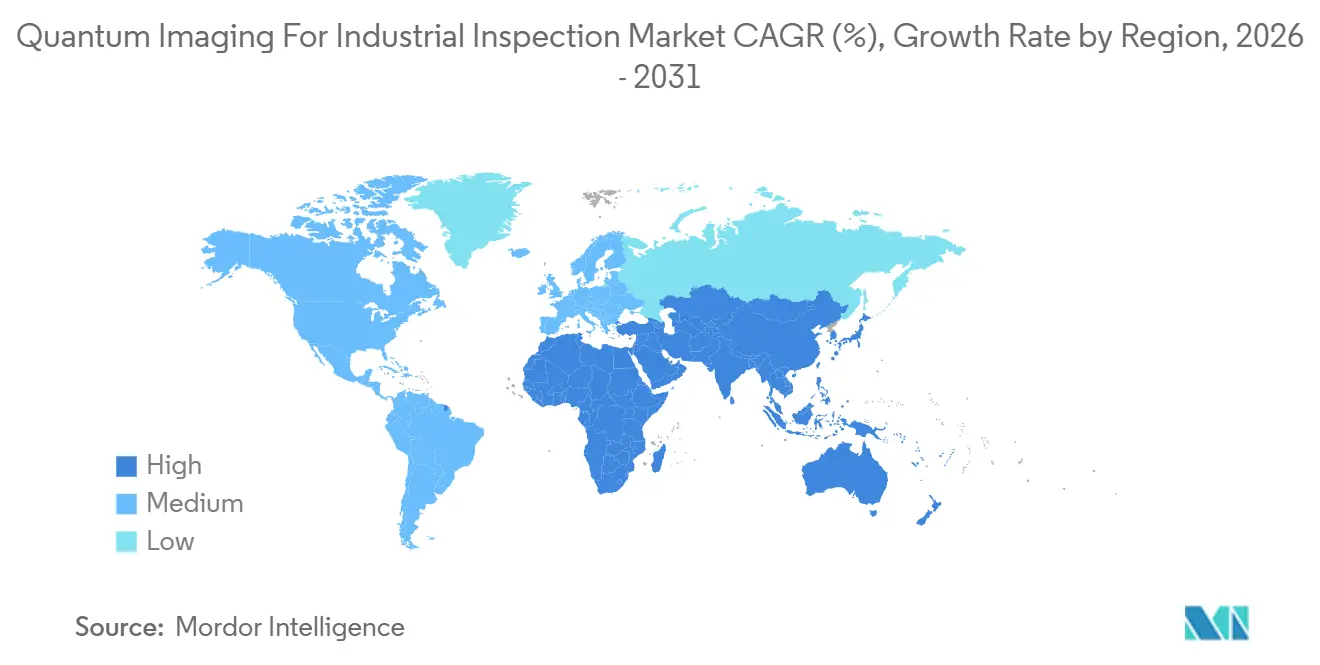
| Fastest Growing Market | Asia-Pacific |
| Largest Market | Asia-Pacific |
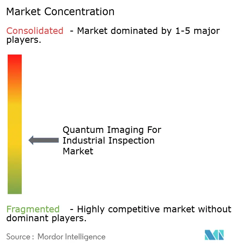
| Market Concentration | Medium |
Major Players *Disclaimer: Major Players sorted in no particular order Image © Mordor Intelligence. Reuse requires attribution under CC BY 4.0. | |
Quantum Imaging For Industrial Inspection Market Analysis by Mordor Intelligence
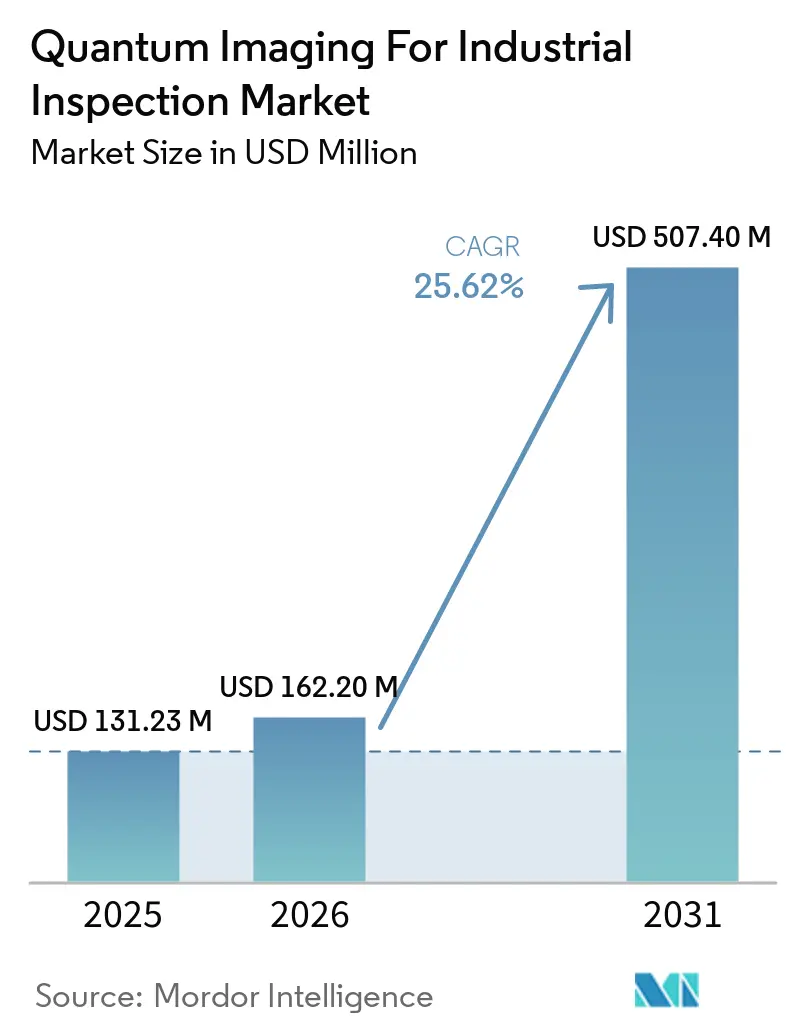
The Quantum Imaging for Industrial Inspection Market size was valued at USD 131.23 million in 2025 and estimated to grow from USD 162.20 million in 2026 to reach USD 507.40 million by 2031, at a CAGR of 25.62% during the forecast period (2026-2031). Growth reflects the need to find smaller defects as semiconductor designs move below 3 nm and packaging becomes more complex. Quantum-enhanced systems address limits in conventional optical inspection for multilayer packages and low-contrast defects. Early adoption is centered on semiconductor manufacturing, where yield protection can justify specialized inspection equipment. The opportunity will broaden as systems become easier to integrate with production environments. High equipment cost and specialist shortages will keep adoption uneven across industrial users during the forecast period.
Key Report Takeaways
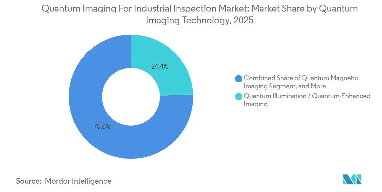
- By quantum imaging technology, Quantum Illumination / Quantum-Enhanced Imaging accounted for 24.41% of the Quantum Imaging for Industrial Inspection Market share in 2025, while Quantum Ghost Imaging is projected to expand at a 26.83% CAGR through 2031.
- By application, Surface Defect Detection accounted for 23.45% of the Quantum Imaging for Industrial Inspection Market size in 2025, while Advanced Packaging and Interconnect Inspection is expected to expand at a 27.56% CAGR through 2031.
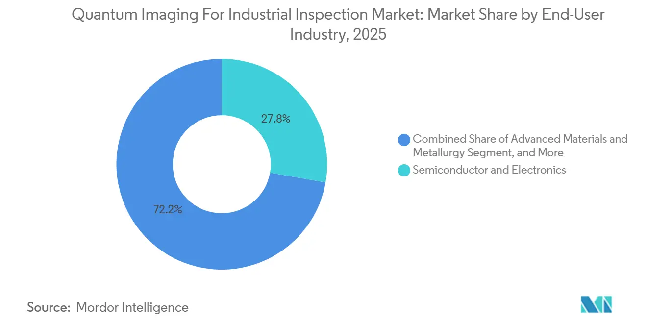
- By end-user industry, Semiconductor and Electronics held 27.76% share in 2025 and is projected to grow at a 26.84% CAGR through 2031.
- By deployment mode, Laboratory and Offline Inspection held 38.89% share in 2025, while In-Line and Production-Line Inspection are projected to expand at a 27.31% CAGR through 2031.
- By geography, Asia-Pacific held 31.24% share in 2025 and is projected to grow at a 27.13% CAGR through 2031.
Note: Market size and forecast figures in this report are generated using Mordor Intelligence’s proprietary estimation framework, updated with the latest available data and insights as of January 2026.
Global Quantum Imaging For Industrial Inspection Market Trends and Insights
Drivers Impact Analysis*
| Driver | (~) % Impact on CAGR Forecast | Geographic Relevance | Impact Timeline |
|---|---|---|---|
| Zero-Defect Manufacturing in Advanced Semiconductor Packaging | +6.4% | Global, concentrated in Asia-Pacific, Taiwan, South Korea, and Japan, and North America | Short term (≤ 2 years) |
| Non-Destructive Inspection of Buried and Subsurface Defects | +5.1% | Global, strongest in Asia-Pacific and North America | Medium term (2-4 years) |
| Inline Inspection and Industrial Automation | +4.2% | Asia-Pacific, North America, and Europe | Medium term (2-4 years) |
| Traceability and Functional-Safety Requirements | +3.0% | North America and Europe, with spillover to Asia-Pacific | Medium term (2-4 years) |
| Quantum Advantage in Low-Light and Low-Reflectance Inspection | +2.3% | Global | Long term (≥ 4 years) |
| Commercialization of Room-Temperature Quantum Sensors | +1.8% | Global, with early adoption in Europe and North America | Long term (≥ 4 years) |
| Source: Mordor Intelligence | |||
Zero-Defect Manufacturing in Advanced Semiconductor Packaging
Advanced packages use HBM stacks, 2.5D silicon interposers, chiplets, and through-silicon vias. Each added interface can introduce a defect that reduces package yield. A void in a microbump layer or an open circuit in a buried interconnect can make a completed package unusable. Conventional optical inspection and X-ray methods do not always provide non-destructive visibility into current flows below the interconnect level. QuantumDiamonds stated that its QDm.1 platform localizes electrical opens in 2.5D and 3D integrated-circuit packages with micron-level accuracy in minutes. Higher yield has a direct operational value for high-volume manufacturers, supporting demand for the Quantum Imaging for Industrial Inspection Market.
Demand for Non-Destructive Inspection of Buried and Subsurface Defects
Cracks below coatings, corrosion, composite delamination, and weld voids have traditionally been examined with ultrasonic testing or X-ray methods. These methods can have resolution limits when defects sit at depth or in complex structures. Quantum magnetic imaging and quantum-enhanced terahertz imaging can examine optically opaque materials without contact or ionizing radiation. Fraunhofer EMFT used a quantum diamond microscope in its APECS pilot line during 2025 and described a widefield measurement that images an entire sample area at once.[1]Fraunhofer EMFT, “Quantendiamantmikroskop Am Fraunhofer EMFT,” FMD.insight, fmd-insight.de The room-temperature approach can reduce practical barriers compared with systems that require cryogenic operation. SiC and GaN power devices create a related inspection need in electric vehicle drivetrains and grid inverters.
Expansion of Inline Inspection and Industrial Automation
Manufacturers are seeking inspection systems that can operate at production-line speed instead of relying on intermittent sampling. Labor costs and zero-defect quality requirements support this move across advanced electronics and automotive manufacturing. Laboratory and Offline Inspection held 38.89% of 2025 revenue, while In-Line and Production-Line Inspection is projected to grow at a 27.31% CAGR through 2031. Quantum sensors must still tolerate vibration and thermal variation before they can operate reliably on many production lines. QuantumDiamonds has described a roadmap from laboratory defect localization to fab-scale metrology in 2027 and inline wafer mapping from 2028 onward. Early production qualifications could create switching costs because inspection tools are often retained through long replacement cycles.
Stricter Traceability and Functional-Safety Requirements
Automotive electrification and aerospace composites increase the consequences of a missed defect. A microvoid in a GaN power module or delamination in an airframe component can create a safety concern. ISO 26262 and airborne system requirements call for documented defect-detection processes and traceable records. Quantum imaging can produce non-destructive records, including magnetic field maps, current-density distributions, and spectral signatures. These outputs can be incorporated into manufacturing execution system records when integration is managed effectively. This strengthens the case for the Quantum Imaging for Industrial Inspection Market in applications where quality documentation is part of the procurement decision.
Restraints Impact Analysis*
| Restraint | (~) % Impact on CAGR Forecast | Geographic Relevance | Impact Timeline |
|---|---|---|---|
| High System Cost and Limited Production-Scale Qualification | -3.7% | Global, most acute outside semiconductor centers in South America and Africa | Medium term (2-4 years) |
| Shortage of Quantum-Optics and Quantum-Metrology Specialists | -1.8% | Global, particularly severe in South America, the Middle East, and Africa | Medium term (2-4 years) |
| Integration Friction With Existing Manufacturing Execution Systems | -1.3% | Global, most pronounced in mature industrial economies with legacy infrastructure | Medium term (2-4 years) |
| Sensitivity to Vibration, Magnetic Interference, and Calibration Conditions | -0.7% | Global, especially relevant for field and at-line deployment | Long term (≥ 4 years) |
| Source: Mordor Intelligence | |||
High System Cost and Limited Production-Scale Qualification
Laboratory-grade quantum inspection platforms are priced in the low- to mid-single-digit million USD range. Proposed inline systems can reach USD 10 million to USD 15 million. These prices fit the capital equipment budgets of large semiconductor manufacturers more readily than those of smaller automotive suppliers, food processors, and metallurgy facilities. Semiconductor fabs also require 6 to 18 months of continuous qualification data before a new inspection method is added to a certified process flow. This creates a delay between technical validation and commercial-scale revenue. The Bavarian State Ministry for Economic Affairs supported a EUR 152 million (USD 165 million) investment for QuantumDiamonds’ Munich facility, intended to expand production capacity. The pace of cost reduction will influence how quickly use extends beyond semiconductor applications.
Shortage of Quantum-Optics and Quantum-Metrology Specialists
Quantum imaging requires skills that combine sensor physics with factory process knowledge. Deployment teams must calibrate systems and determine whether a signal identifies a meaningful defect. This expertise has only recently started to move from physics departments into engineering applications. Hamamatsu Photonics provides application resources for its ORCA-Quest 2 qCMOS camera and multi-pixel photon counter portfolio. Wider adoption will require practical collaboration between industry and academic programs. Without a larger specialist base, customization and on-site support may delay deployments in the Quantum Imaging for Industrial Inspection Market.
*Our forecasts treat driver/restraint impacts as directional, not additive. The impact forecasts reflect baseline growth, mix effects, and variable interactions.
Segment Analysis
By Quantum Imaging Technology: Quantum Illumination Leads, Ghost Imaging Accelerates
Quantum Illumination and Quantum-Enhanced Imaging held 24.41% of the Quantum Imaging for Industrial Inspection Market share in 2025. Its lead reflected a lower integration complexity than that of many entanglement-dependent approaches. The technology can work with established optical inspection infrastructure. It also improves signal-to-noise performance for low-reflectance materials without cryogenic operation. These characteristics make it a practical initial option for manufacturers evaluating quantum-enhanced inspection. Its position shows why compatibility with existing factory equipment remains important within the Quantum Imaging for Industrial Inspection Market.
Quantum Ghost Imaging is projected to record the highest technology CAGR of 26.83% through 2031. Its earlier commercialization barrier was slow image acquisition. The technique can support the inspection of absorptive or thermally sensitive materials, where standard illumination may damage samples or produce false signals. Single-Photon and Photon-Counting Imaging remains another major technology cluster, with Hamamatsu’s ORCA-Quest 2 positioned for photon-number-resolving scientific imaging.[2]Hamamatsu Photonics, “Hamamatsu Develops ThermoDynamic Imaging Technology for PHEMOS-X Series,” Hamamatsu Photonics, hamamatsu.com Peer-reviewed work reported SPAD array-based quantum ghost imaging at 1 Hz frame rates, bringing the method closer to industrially useful timescales.



By Application: Surface Defect Detection Anchors Revenue While Packaging Inspection Accelerates
Surface Defect Detection held 23.45% of the Quantum Imaging for Industrial Inspection Market size in 2025. Its position reflects established demand in semiconductor wafer inspection, metal surface verification, and coated-material characterization. Surface inspection benefits when systems can distinguish low-contrast boundaries with greater signal quality. It also fits applications where defects are visible but difficult to classify reliably. Semiconductor research on optical inspection at the 2 nm and 1.4 nm technology nodes shows continued pressure to improve detection sensitivity. Surface use cases provide a current revenue base, while other applications are in qualification.
Advanced Packaging and Interconnect Inspection is projected to expand at a 27.56% CAGR through 2031. HBM, chiplet, and glass interposer integration are increasing the number of buried interfaces that affect yield. These interfaces cannot always be assessed with established inspection methods. QuantumDiamonds deployed a QDm.1 quantum diamond microscopy system at Integrated Service Technology in Hsinchu during 2026 for advanced packaging failure analysis. Semiconductor Failure Analysis remains aligned with current laboratory capabilities because the workflow can accommodate lower throughput. Subsurface Crack and Corrosion Detection and Weld, Joint, and Composite Inspection are gaining relevance in aerospace and automotive manufacturing. Process Monitoring and Inline Quality Control has a longer adoption path because it depends on reliable production-line integration.
By End-User Industry: Semiconductor Sector Sustains Dual Leadership in Share and Growth
Semiconductor and Electronics held 27.76% of the Quantum Imaging for Industrial Inspection Market share in 2025. It is also projected to grow at the fastest end-user CAGR of 26.84% through 2031. The combination indicates that use in this sector remains far from mature. Manufacturers are facing rising defect-detection requirements as process nodes advance and three-dimensional packages become more complex. Classical optical tools face diffraction-related limits below 3 nm. Quantum-enhanced techniques offer a route to stronger inspection sensitivity for these demanding applications.
Automotive and E-Mobility is the next important end-user area because SiC and GaN devices are used in electric drivetrains and onboard chargers. Aerospace and Defense demand centers on composite integrity and avionics component verification. Energy, Oil and Gas, and Nuclear operators can use non-destructive approaches to inspect through coatings and thick-walled equipment without ionizing radiation. Advanced Materials and Metallurgy, Pharmaceuticals and Life Sciences Manufacturing, and Food and Agriculture Processing have identifiable use cases. These include tablet contamination detection, grain-quality imaging, and additive-manufactured part verification. Their longer deployment timelines reflect equipment qualification and quality-management requirements rather than a lack of potential applications.
By Deployment Mode: Laboratory Dominance Gives Way to a Production-Line Transition
Laboratory and Offline Inspection held 38.89% of the Quantum Imaging for Industrial Inspection Market share in 2025. This lead reflects how commercial platforms first entered failure-analysis laboratories and university settings. Sample-based testing can work with the throughput limits of current laboratory-grade systems. At-Line Inspection sits near the production line and can return results faster than an offline laboratory process. It does not require the full integration of inline operation. Field and Portable Inspection remains the smallest category in 2026 because quantum sensors remain sensitive to environmental conditions.
In-Line and Production-Line Inspection is projected to grow at a 27.31% CAGR through 2031. This mode could concentrate more value once platforms meet factory requirements for throughput, uptime, and vibration tolerance. QuantumDiamonds has set out a path from current laboratory localization to fab-scale defect metrology in 2027 and 100% inline wafer mapping after 2028. Bosch reported a February 2025 laboratory sensitivity record for an NV-center magnetometer at 100 million times below Earth’s magnetic field strength. Such progress is relevant to room-temperature sensing under ambient conditions. Production qualification will remain more demanding than the earlier move from offline to inline optical inspection.
Geography Analysis
Asia-Pacific held 31.24% of the Quantum Imaging for Industrial Inspection Market share in 2025 and is projected to grow at a 27.13% CAGR through 2031. Taiwan, South Korea, Japan, and China concentrate a large share of advanced semiconductor fabrication. Taiwan is an early deployment location because it supports leading-edge logic manufacturing. QuantumDiamonds installed its QDm. 1 system at Integrated Service Technology in Hsinchu during 2026 and opened an Asian headquarters in Taiwan. South Korea’s HBM memory ecosystem is a separate demand center because stacked memory creates buried bond-interface defects. China is also developing domestic interest in NV-center imaging through packaging companies and university research programs.
North America held the second-largest revenue share in the Quantum Imaging for Industrial Inspection Market. The United States combines semiconductor design companies, advanced packaging subcontractors, defense laboratories, and university quantum programs. New fab construction in Arizona, Ohio, and Texas creates future procurement cycles as sites reach production scale. QuantumDiamonds completed its first US deployment at Eurofins EAG Laboratories in Sunnyvale during 2026. The installation provides a visible reference site for failure-analysis laboratories considering the technology. Canada’s quantum research clusters and Mexico’s electronics manufacturing corridor are earlier-stage demand areas in the forecast period.
Europe ranked third by revenue share but has active policy support for commercialization. The Bavarian State Ministry for Economic Affairs described QuantumDiamonds’ Munich site as a dedicated production line for quantum-based semiconductor testing systems.[3]Bavarian State Ministry for Economic Affairs, Energy and Technology, “Aiwanger: Die Weltweit Erste Produktionslinie Für Quantenbasierte Halbleiter-Prüfsysteme Ist Ein Meilenstein Für Den Hightech-Standort Bayern,” Bavarian State Ministry for Economic Affairs, stmwi.bayern.de Germany, the United Kingdom, France, and the Netherlands host much of the region’s quantum-sensing research and early commercialization. Fraunhofer EMFT’s 2025 APECS pilot-line deployment demonstrates the role of publicly funded infrastructure in building industrial readiness. South America, the Middle East, and Africa remain nascent regions. Oil and gas testing in the Middle East and subsurface materials work in South Africa offer initial use cases, while broader adoption is likely to depend on lower costs and deeper specialist pools after 2028.

Competitive Landscape
The Quantum Imaging for Industrial Inspection Market is moderately fragmented at the system level. Competition includes deep-technology companies and established scientific instrumentation suppliers that are adding quantum sensing capabilities. The company received EUR 91 million (USD 104.1 million) in financing during 2026 for production and international expansion.[4]Technical University of Munich School of Natural Sciences, “QuantumDiamonds Secures EUR 91 Million for Next-Generation Chip Inspection,” Technical University of Munich, nat.tum.de This investment supports its Munich facility and gives it resources to increase manufacturing capacity. The company’s QDm.1 deployments in Taiwan and the United States serve as reference installations in key semiconductor ecosystems.
Competition is shaped by the supply of sensor substrates, deployment modes, and application specialization. Element Six supplies synthetic diamond materials for NV-center applications, while photonics suppliers support SPAD-array approaches. Hamamatsu Photonics supplies photon-counting and scientific imaging equipment for research and early commercial applications. Single Quantum B.V. and AUREA Technology address the single-photon detector layer of the ecosystem. EuQlid commercialized its Qu-MRI quantum magnetometry platform in 2025 for non-destructive mapping of buried electrical current flows. Bosch Quantum Sensing is pursuing ambient-environment NV-center magnetometer performance, which may support later field and inline use cases.
Quantum Design International acquired Qnami in June 2026, bringing the ProteusQ scanning NV microscope and related sensing components into its instrumentation portfolio. In January 2026, Quantum Design International acquired the NanoScience division of Oxford Instruments. These transactions show that larger platforms are using acquisitions to add specialized quantum capabilities. Oxford Instruments reported 12.7% organic constant-currency order growth in semiconductor-related applications for fiscal year 2026. Field-portable inspection and industrial use outside semiconductors remain open areas because commercially qualified systems are limited.
Quantum Imaging For Industrial Inspection Industry Leaders
QuantumDiamonds GmbH
Qnami AG
QDI Systems B.V.
Bosch Quantum Sensing GmbH
TR2 SRLS
- *Disclaimer: Major Players sorted in no particular order

Recent Industry Developments
- July 2026: The Bavarian State Ministry for Economic Affairs publicly endorsed QuantumDiamonds' Munich production facility as the world's first dedicated production line for quantum-based semiconductor testing systems, framing the investment as a milestone for high-technology industrial development in the region.
- June 2026: Quantum Design International completed the acquisition of Qnami, the Basel-based pioneer in diamond NV center scanning probe microscopy. The transaction integrates Qnami's ProteusQ scanning NV microscope and quantum sensing component portfolio into Quantum Design's global scientific instrumentation network and pairs it with the NanoScience capabilities acquired from Oxford Instruments in January 2026.
- March 2026: QuantumDiamonds completed its first Asian commercial deployment at Integrated Service Technology in Hsinchu, Taiwan, establishing a reference installation within Taiwan's central semiconductor manufacturing cluster and marking the company's entry into Asia's advanced packaging failure analysis market.
- January 2026: Quantum Design International acquired the NanoScience division of Oxford Instruments, consolidating cryogenic quantum characterization and NV magnetometry assets into a single portfolio serving quantum materials research, semiconductor characterization, and advanced device inspection markets globally.


Global Quantum Imaging For Industrial Inspection Market Report Scope
The quantum imaging for industrial inspection market includes technologies that use quantum properties of light, such as entanglement and photon correlation, to capture high-resolution images and detect defects in industrial components and materials. These solutions support non-destructive testing, quality control, and precision inspection across manufacturing, aerospace, automotive, electronics, and other industrial applications.
The Quantum Imaging for Industrial Inspection Market Report is Segmented by Quantum Imaging Technology (Quantum Illumination / Quantum-Enhanced Imaging, Single-Photon / Photon-Counting Imaging, Quantum Ghost Imaging, Quantum-Enhanced Interferometric Imaging, Quantum Magnetic Imaging, and Other Quantum Imaging Technologies), Application (Surface Defect Detection, Subsurface Crack and Corrosion Detection, Semiconductor Failure Analysis, Advanced Packaging and Interconnect Inspection, Weld, Joint, and Composite Inspection, Process Monitoring and Inline Quality Control, and Other Applications), End-User Industry (Semiconductor and Electronics, Automotive and E-Mobility, Aerospace and Defence, Energy, Oil and Gas, and Nuclear, Advanced Materials and Metallurgy, Pharmaceuticals and Life Sciences Manufacturing, Food and Agriculture Processing, and Other End-User Industries), Deployment Mode (In-Line / Production-Line Inspection, At-Line Inspection, Laboratory / Offline Inspection, and Field / Portable Inspection), and Geography (North America, South America, Europe, Asia-Pacific, Middle East, and Africa). The Market Forecasts are Provided in Terms of Value (USD).
| Quantum Illumination / Quantum-Enhanced Imaging |
| Single-Photon / Photon-Counting Imaging |
| Quantum Ghost Imaging |
| Quantum-Enhanced Interferometric Imaging |
| Quantum Magnetic Imaging |
| Other Quantum Imaging Technologies |
| Surface Defect Detection |
| Subsurface Crack and Corrosion Detection |
| Semiconductor Failure Analysis |
| Advanced Packaging and Interconnect Inspection |
| Weld, Joint, and Composite Inspection |
| Process Monitoring and Inline Quality Control |
| Other Applications |
| Semiconductor and Electronics |
| Automotive and E-Mobility |
| Aerospace and Defence |
| Energy, Oil and Gas, and Nuclear |
| Advanced Materials and Metallurgy |
| Pharmaceuticals and Life Sciences Manufacturing |
| Food and Agriculture Processing |
| Other End-User Industries |
| In-Line / Production-Line Inspection |
| At-Line Inspection |
| Laboratory / Offline Inspection |
| Field / Portable Inspection |
| North America | United States |
| Canada | |
| Mexico | |
| South America | Brazil |
| Argentina | |
| Chile | |
| Rest of South America | |
| Europe | Germany |
| United Kingdom | |
| France | |
| Italy | |
| Spain | |
| Rest of Europe | |
| Asia-Pacific | China |
| Japan | |
| India | |
| South Korea | |
| Australia | |
| Rest of Asia-Pacific | |
| Middle East | United Arab Emirates |
| Saudi Arabia | |
| Qatar | |
| Rest of Middle East | |
| Africa | South Africa |
| Egypt | |
| Nigeria | |
| Rest of Africa |
| By Quantum Imaging Technology | Quantum Illumination / Quantum-Enhanced Imaging | |
| Single-Photon / Photon-Counting Imaging | ||
| Quantum Ghost Imaging | ||
| Quantum-Enhanced Interferometric Imaging | ||
| Quantum Magnetic Imaging | ||
| Other Quantum Imaging Technologies | ||
| By Application | Surface Defect Detection | |
| Subsurface Crack and Corrosion Detection | ||
| Semiconductor Failure Analysis | ||
| Advanced Packaging and Interconnect Inspection | ||
| Weld, Joint, and Composite Inspection | ||
| Process Monitoring and Inline Quality Control | ||
| Other Applications | ||
| By End-User Industry | Semiconductor and Electronics | |
| Automotive and E-Mobility | ||
| Aerospace and Defence | ||
| Energy, Oil and Gas, and Nuclear | ||
| Advanced Materials and Metallurgy | ||
| Pharmaceuticals and Life Sciences Manufacturing | ||
| Food and Agriculture Processing | ||
| Other End-User Industries | ||
| By Deployment Mode | In-Line / Production-Line Inspection | |
| At-Line Inspection | ||
| Laboratory / Offline Inspection | ||
| Field / Portable Inspection | ||
| By Geography | North America | United States |
| Canada | ||
| Mexico | ||
| South America | Brazil | |
| Argentina | ||
| Chile | ||
| Rest of South America | ||
| Europe | Germany | |
| United Kingdom | ||
| France | ||
| Italy | ||
| Spain | ||
| Rest of Europe | ||
| Asia-Pacific | China | |
| Japan | ||
| India | ||
| South Korea | ||
| Australia | ||
| Rest of Asia-Pacific | ||
| Middle East | United Arab Emirates | |
| Saudi Arabia | ||
| Qatar | ||
| Rest of Middle East | ||
| Africa | South Africa | |
| Egypt | ||
| Nigeria | ||
| Rest of Africa | ||


Key Questions Answered in the Report
What is the size of the Quantum Imaging for Industrial Inspection Market?
The Quantum Imaging for Industrial Inspection Market is estimated at USD 162.20 million in 2026 and is forecast to reach USD 507.40 million by 2031 at a 25.62% CAGR.
Which technology is growing fastest in quantum imaging for industrial inspection?
Quantum Ghost Imaging is projected to expand at a 26.83% CAGR through 2031, supported by faster SPAD-array image acquisition.
Which application leads the adoption of quantum imaging systems?
Surface Defect Detection held the largest application share at 23.45% in 2025, while Advanced Packaging and Interconnect Inspection is projected to grow fastest.
Why do semiconductor manufacturers use quantum inspection?
The systems support non-destructive detection of difficult defects in advanced nodes, HBM stacks, chiplets, and buried interconnects. For the Quantum Imaging for Industrial Inspection Market, this makes failure analysis an important entry point before systems move into continuous production monitoring.
Which region is leading adoption?
Asia-Pacific held 31.24% share in 2025 and is projected to record a 27.13% CAGR through 2031. The region leads the Quantum Imaging for Industrial Inspection Market because Taiwan, South Korea, Japan, and China have dense semiconductor manufacturing and packaging activity.
What limits wider deployment of quantum inspection equipment?
High system prices, lengthy production qualification, specialist shortages, and factory-integration requirements limit broader near-term deployment. These limits keep the Quantum Imaging for Industrial Inspection Market focused on large semiconductor users, while smaller industrial users remain in earlier evaluation stages.
Page last updated on: