Quantum-Dot SWIR Imaging Systems Market Size and Share
Market Overview
| Study Period | 2020 - 2031 |
|---|---|
| Market Size (2026) | USD 54.09 Million |
| Market Size (2031) | USD 95.88 Million |
| Growth Rate (2026 - 2031) | 12.13 % |
| Fastest Growing Market | Asia-Pacific |
| Largest Market | Asia-Pacific |
| Market Concentration | High |
Major Players *Disclaimer: Major Players sorted in no particular order Image © Mordor Intelligence. Reuse requires attribution under CC BY 4.0. | |
Quantum-Dot SWIR Imaging Systems Market Analysis by Mordor Intelligence
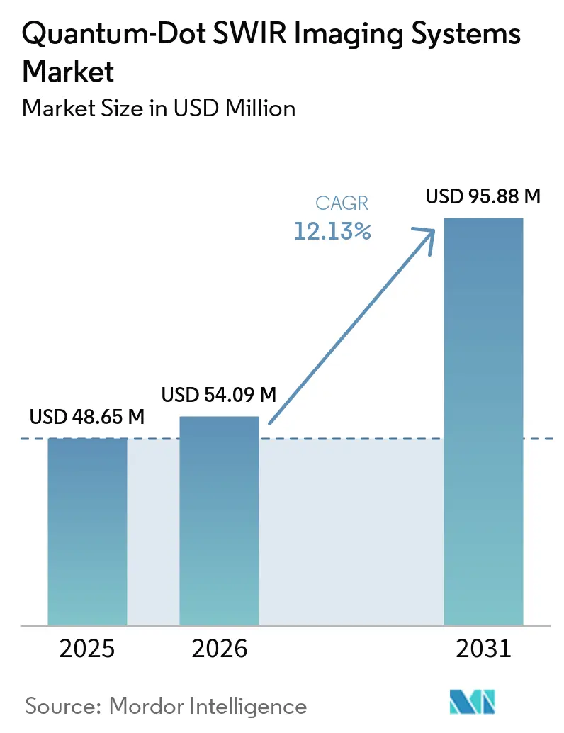
The Quantum-dot SWIR imaging systems market size is projected to expand from USD 48.65 million in 2025 to USD 54.09 million in 2026, and to USD 95.88 million by 2031, registering a CAGR of 12.13% between 2026 and 2031. Lower-cost quantum-dot deposition on CMOS readout circuits is widening access to industrial inspection, sorting, and UAV monitoring applications that were less viable with InGaAs systems. Semiconductor investment in the United States, Japan, South Korea, and China is supporting demand for inspection tools that can image through silicon. Suppliers are pairing sensor development with packaging, spectral tuning, and software to reduce barriers to system integration. The Quantum-dot SWIR imaging systems market also faces limits in thin-film uniformity, signal quality, and qualification requirements for precision applications. These factors favor suppliers that can prove reliability while offering lower ownership costs and application-specific performance.
Key Report Takeaways
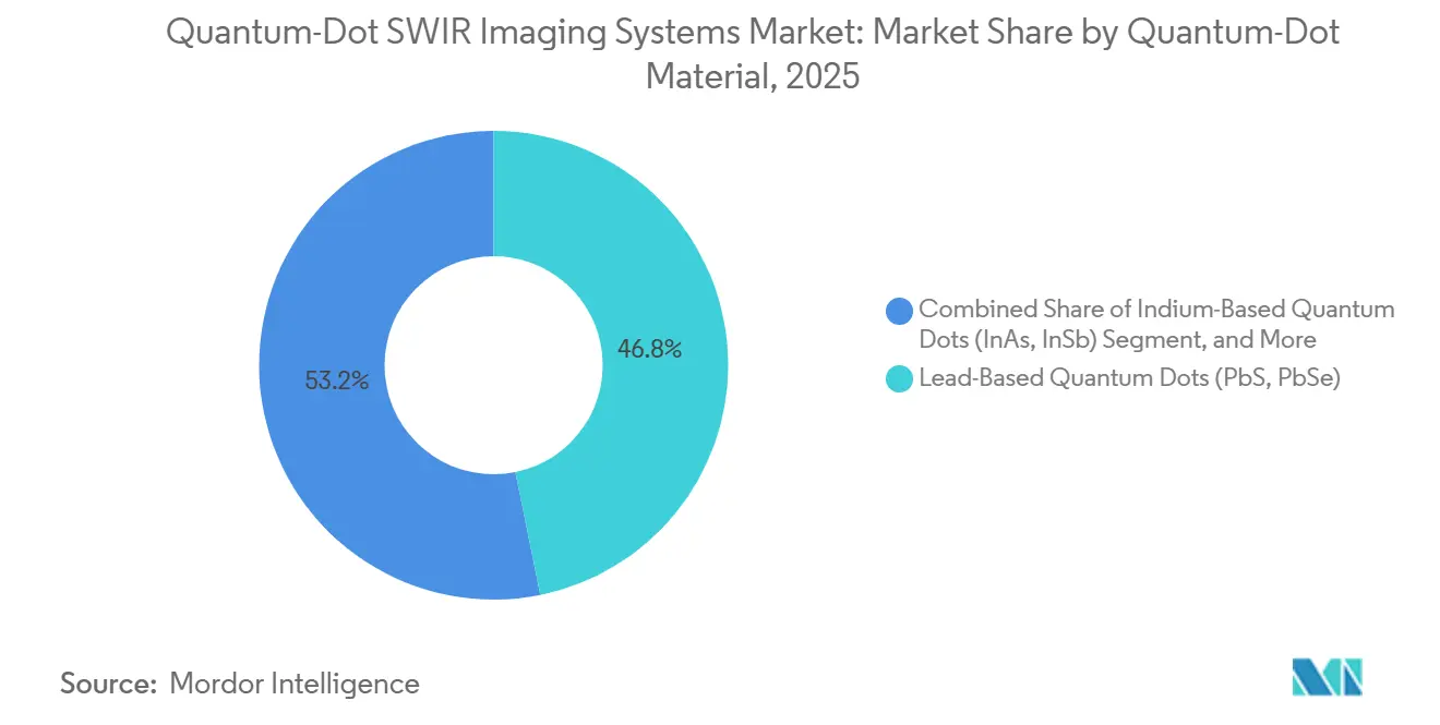
- By quantum-dot material, lead-based quantum dots held 46.81% Quantum-Dot SWIR Imaging Systems Market revenue share in 2025, while indium-based quantum dots recorded the highest projected CAGR at 15.91% through 2031.
- By product type, SWIR cameras accounted for 41.63% of revenue in 2025, while custom and OEM sensor platforms are forecast to grow at a 14.23% CAGR through 2031.
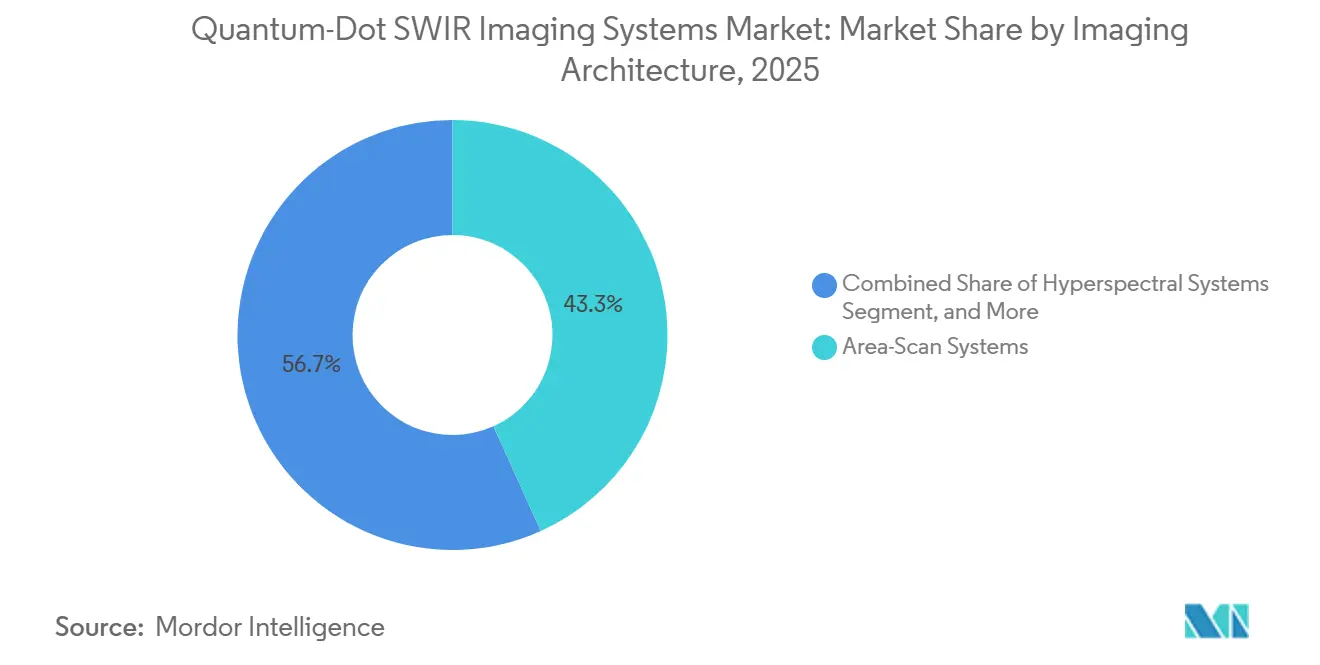
- By imaging architecture, area-scan systems held 43.27% revenue share in the Quantum-Dot SWIR Imaging Systems Market in 2025, while hyperspectral systems are projected to expand at a 15.83% CAGR through 2031.
- By end-user industry, industrial manufacturing held 27.43% revenue share in 2025, while automotive and mobility are forecast to grow at 15.63% CAGR through 2031.
- By geography, Asia-Pacific held 38.71% of the Quantum-Dot SWIR Imaging Systems Market in 2025 and is forecast to grow at a CAGR of 14.83% through 2031.
Note: Market size and forecast figures in this report are generated using Mordor Intelligence’s proprietary estimation framework, updated with the latest available data and insights as of January 2026.
Market Trends and Insights
Drivers Impact Analysis of Quantum-Dot SWIR Imaging Systems Market*
| Driver | (~) % Impact on CAGR Forecast | Geographic Relevance | Impact Timeline |
|---|---|---|---|
| Lower Cost per Megapixel From QD-on-CMOS Integration | +3.5% | Global, with stronger demand in Asia-Pacific industrial corridors and North American semiconductor fabs | Short term (≤ 2 years) |
| High-Resolution and Small-Pixel Imaging Demand | +2.8% | North America and Europe for metrology and defense, and Asia-Pacific chipmaker lines | Medium term (2-4 years) |
| Semiconductor Wafer Inspection and Material Identification | +2.2% | China, South Korea, Japan, and North American fab expansion zones | Short term (≤ 2 years) |
| Food, Plastic, and Agricultural Sorting Automation | +1.8% | Europe, Asia-Pacific, and North America | Medium term (2-4 years) |
| Silicon-Fab Compatibility and Spectral Customization | +1.4% | North America, Europe, and Asia-Pacific CMOS pilot lines | Long term (≥ 4 years) |
| Edge AI Integration in Compact Autonomous Platforms | +1.0% | Global, with early adoption in Asia-Pacific automotive and European drone applications | Medium term (2-4 years) |
| Source: Mordor Intelligence | |||
Lower Cost per Megapixel From QD-on-CMOS Integration
QD-on-CMOS manufacturing eliminates the indium phosphide substrate-bonding step used in InGaAs sensors. Instead, it uses solution processing on standard CMOS foundry infrastructure, including spin coating or inkjet deposition directly onto the readout circuit. Quantum Solutions stated that this approach can move chip costs from more than USD 5,000 toward low triple-digit levels at commercial volume. A 2,048×2,048-pixel colloidal quantum dot sensor on a commercial 0.18-µm CMOS process, operating at 30 fps with a 10 µm pixel pitch. Emberion reported 100% bond yield across 100 sensors on a full wafer and targeted a packaged sensor cost of EUR 50 (USD 54) at scale. The lower process burden can shorten the route from sensor fabrication to packaged products. This cost reduction can expand the Quantum-dot SWIR imaging systems market among customers who need production-line inspection but cannot justify the costs of conventional InGaAs systems.
High-Resolution and Small-Pixel Imaging Demand
Machine-vision customers need small pixels for subsurface semiconductor defects and pharmaceutical tablet inspection. Legacy InGaAs arrays can face alignment constraints as pixel dimensions decline because their detectors and readout circuits require hybrid assembly. A PbS quantum-dot sensor achieved monolithic fabrication at 640×512 pixels on a silicon ROIC and an average detectivity of 1.7×10¹⁰ Jones. The device avoided flip-chip bonding through a planar p-n homojunction architecture. Imec integrated colloidal quantum-dot photodiodes with metasurfaces on a 300 mm CMOS pilot line in December 2025. This approach could shift spectral customization from absorber reformulation to lithography, helping suppliers tailor sensors for the Quantum-dot SWIR imaging systems market without redesigning the full detector stack.
Semiconductor Wafer Inspection and Material Identification
SWIR wavelengths can be used to image through silicon and III-V wafers without photodamage. This supports the detection of bonding voids, alignment marks, and defects that visible imaging cannot resolve during manufacturing or assembly. Allied Vision identifies SWIR imaging as relevant to semiconductor wafer inspection and advanced packaging workflows. Basler demonstrated SWIR-supported wafer bonding and alignment at 1 µm precision. QD-based sensors can add spectral tuning to this silicon-penetration capability. A single system may therefore inspect silicon, gallium nitride, and silicon carbide without mechanical filter changes, supporting demand across the Quantum-dot SWIR imaging systems market.
Food, Plastic, and Agricultural Sorting Automation
SWIR imaging identifies molecular absorption bands that support non-destructive material sorting. Water absorbs at 1,200 nm, 1,450 nm, and 1,920 nm, while lipid bonds absorb within the 1,700-1,900 nm range. These signatures support quality checks that visible and near-infrared cameras cannot replicate on fast-moving materials. Teledyne DALSA introduced its Kaleido SWIR hyperspectral camera in May 2026 with up to 1,280-pixel spatial resolution and line rates above 2.3 kHz. The HyperImage project reported 10-20% yield improvement in vertical farming and 20% fuel saving in autonomous vehicles using SWIR-enabled navigation. These operating benefits support the adoption of Quantum-dot SWIR imaging systems across recycling, food safety, and agricultural workflows.[1]HyperImage, A Universal Spectral Imaging Sensor Platform for Industry, Agriculture and Autonomous Driving,” European Commission CORDIS, cordis.europa.eu.
Restraints Impact Analysis of Quantum-Dot SWIR Imaging Systems Market*
| Restraint | (~) % Impact on CAGR Forecast | Geographic Relevance | Impact Timeline |
|---|---|---|---|
| High Qualification Costs Versus InGaAs Incumbents | -2.0% | North America and Europe, particularly defense, aerospace, and precision metrology | Short term (≤ 2 years) |
| Signal-to-Noise and Temperature Stability Trade-Offs | -1.3% | Global, with greater exposure in North American and European high-precision applications | Medium term (2-4 years) |
| Lead-Based Quantum-Dot Toxicity and End-of-Life Compliance | -0.8% | Europe and global OEM supply chains | Medium term (2-4 years) |
| Thin-Film Uniformity and ROIC Planarity at Volume | -0.5% | Global wafer-fabrication hubs in Asia-Pacific and North America | Long term (≥ 4 years) |
| Source: Mordor Intelligence | |||
High Qualification Costs Versus InGaAs Incumbents
Defense and precision metrology customers often require 18-36 months of environmental testing, reliability validation, and supply chain audits. These processes can cost several million USD under MIL-STD-810 and related requirements. InGaAs platforms have long operating histories, making procurement teams reluctant to change suppliers until reliability is proven across the full operating envelope. Fully built, cooled high-dynamic-range cameras can exceed USD 20,000 in list price. Emberion reported that its wafer-level packaging process met MIL-spec hermeticity in initial testing and was planned for commercial camera products in 2026. Industrial buyers can validate products under less demanding conditions and may adopt them earlier. The Quantum-dot SWIR imaging systems market is therefore likely to see commercial and industrial demand before it sees comparable defense and metrology volumes.[2]Wide-Dynamic-Range Lead-Free SWIR Image Sensors Based on InAs Thin-Film Quantum-Dot Photodiodes,” Sensors, doi.org.
Signal-to-Noise and Temperature Stability Trade-Offs
CQD photodetectors can have higher dark current density and lower signal-to-noise ratios than epitaxial InGaAs devices at comparable temperatures. This limits its use in low-light surveillance and scientific imaging when cooling is unavailable. PbS quantum-dot photodiodes showed dark current densities from 0.0025 µA/cm² to 100 µA/cm², depending on architecture. High-performance InGaAs diodes maintained values below 0.02 µA/cm² in the same published comparison. Temperature-related movement of the absorption edge also complicates calibration in hyperspectral systems where narrow spectral bands must remain consistent. KAIST reported an 85-fold room-temperature infrared signal gain using avalanche electron amplification in colloidal quantum dots. Progress in amplification and device design could reduce this limitation for the Quantum-dot SWIR imaging systems market.[3]Candidate List of Substances of Very High Concern for Authorisation,” European Chemicals Agency, echa.europa.eu.
*Our forecasts treat driver/restraint impacts as directional, not additive. The impact forecasts reflect baseline growth, mix effects, and variable interactions.
Quantum-Dot SWIR Imaging Systems Market Segment Analysis
By Quantum-Dot Material:
Lead-Based Platforms Support Volume While Indium Compounds Address ComplianceLead-based quantum dots retained 46.81% of the Quantum-dot SWIR imaging systems market share in 2025. PbS and PbSe benefit from mature colloidal synthesis and established ligand-exchange methods. Their 900 nm-2,000+ nm absorption window supports several commercial SWIR uses and gives the Quantum-dot SWIR imaging systems market a well-established material base. A PbS synthesis process using recovered PbCl₂ from spent lead-acid batteries achieved a 97% recovery rate. The process also reduced production costs by 23.2% compared with commercial PbCl₂. This route may preserve the competitiveness of lead-based materials while end-of-life requirements become more demanding.
Indium-based quantum dots are projected to grow at 15.91% CAGR through 2031. Their lead-free profile is relevant to consumer, medical, and automotive supply chains. An InAs thin-film QD sensor delivered 28% external quantum efficiency at 1,200 nm and 83.5 dB dynamic range. Researchers at Sungkyunkwan University reported a real-time InAs quantum-dot infrared imager with a pixel array and custom ROIC in April 2026. EU Directive 2024/1416 tightened cadmium restrictions, while ECHA listed lead as one of 250 substances of very great concern as of June 2025. Mercury chalcogenide quantum dots remain relevant beyond 2,000 nm, and other materials, such as Ag₂Te, are receiving research attention for sensing applications.[4]Semiconductor Wafer Inspection, SWIR Imaging,” Allied Vision Technologies, alliedvision.com.



By Product Type:
Cameras Lead Revenue While OEM Platforms Deepen IntegrationSWIR cameras accounted for 41.63% of the Quantum-dot SWIR imaging systems market size in 2025. Machine-vision integrators use these systems as turnkey products with embedded image signal processing and validated lens compatibility. GigE Vision and Camera Link interfaces also support deployment in established production environments. Camera cores and modules serve integrators building multispectral rigs. Focal plane arrays and image sensors remain important where buyers need bare-sensor access for customized optics. This product mix lets the Quantum-dot SWIR imaging systems market serve standard installations and specialized research or defense requirements.
Custom and OEM sensor platforms are forecast to expand at 14.23% CAGR through 2031. Automotive Tier 1 suppliers and consumer-electronics ODMs need sensing hardware that can be embedded without a complete camera assembly. TriEye and LITEON made the TES200 CMOS-based SWIR sensor available in samples during August 2025. The chip-level format can reduce housing, cooling, and interface requirements in finished products. SWIR Vision Systems disclosed a multiband focal-plane array that combines microbolometer and CQD SWIR detectors on a single ROIC. Such designs can extend the Quantum-dot SWIR imaging systems industry into thermal and SWIR fusion applications.
By Imaging Architecture:
Area-Scan Systems Lead While Hyperspectral Systems Gain UsesArea-scan systems held 43.27% of the Quantum-dot SWIR imaging systems market share in 2025. They capture a complete spatial frame at one time. This makes them suitable for 2D defect detection, wafer inspection, and industrial surveillance. Line-scan systems are the second-largest architecture group. They are used for paper, textile, and film lines where material moves continuously. Multispectral and snapshot systems held smaller positions but are gaining relevance in handheld and drone-mounted equipment across the Quantum-dot SWIR imaging systems market.
Hyperspectral systems are forecast to grow at 15.83% CAGR through 2031. Lower sensor costs and the availability of chemometric software are improving their fit for recycling and food sorting. Specim's FX19 push-broom camera operates from 1,130-1,920 nm at up to 527 fps and has 640-pixel spatial resolution. Its performance supports inline inspection at conveyor speeds above 3 m/s. Imec's metasurface-integrated quantum-dot photodiodes encode spectral selectivity during CMOS lithography. This could enable snapshot hyperspectral imaging in area-scan hardware and reshape the Quantum-dot SWIR imaging systems market over time.
By End-User Industry:
Industrial Manufacturing Leads While Automotive and Mobility Grows FastestIndustrial manufacturing accounted for 27.43% of the Quantum-dot SWIR imaging systems market in 2025. Inspection of electronics, batteries, and advanced materials is a key source of demand. SWIR material identification can support line yield and process control. Semiconductor and electronics ranked second among end users. Its demand is rising as advanced packaging increases the complexity of inspection. Aerospace and defense also sustain revenue through persistent-surveillance payloads, although qualification cycles slow adoption in the Quantum-dot SWIR imaging systems market.
Automotive and mobility is projected to grow at 15.63% CAGR through 2031. Demand is linked to occupant monitoring, LiDAR illumination detection, and all-weather lane sensing. In April 2026, DGIST demonstrated a 32×32-pixel Ag₂Te quantum dot and MoS₂ hybrid infrared image sensor for fog and night imaging. Food and agriculture are adopting hyperspectral grading beyond premium produce. Healthcare and research institutions purchase focal plane arrays and camera cores for spectral microscopy. Recycling and environmental services require higher plastic-sorting purity, while consumer electronics remain a longer-term opportunity in biometric sensing and XR displays.
Geography Analysis
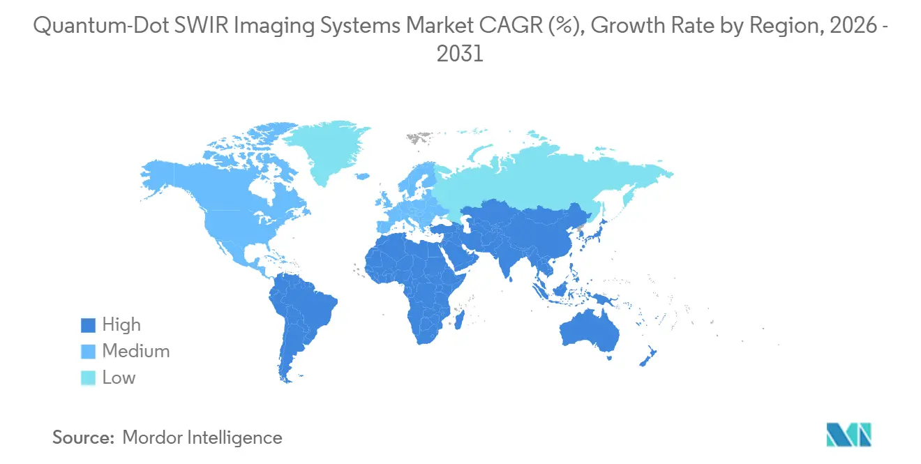
APAC Quantum-Dot SWIR Imaging Systems Market
Asia-Pacific accounted for 38.71% of the Quantum-dot SWIR imaging systems market in 2025 and is projected to grow at a 14.83% CAGR through 2031. China’s semiconductor self-sufficiency effort has increased local demand for wafer inspection. South Korea has progressed from research to production-oriented development. A team from Dong-eui University and Korea University developed a deposition method for 268 ppi QD photodiode arrays without photolithography in August 2025. Gpixel released the GIR1201 and GIR2505 line-scan sensors in Japan during October 2025. The sensors achieved 75% quantum efficiency at 1,550 nm and were targeted for food, recycling, and semiconductor inspection. India is an emerging market with high demand, as domestic electronics manufacturing supports investment in inline quality inspection.
North America Quantum-Dot SWIR Imaging Systems Market
North America is the second-largest regional position in the Quantum-dot SWIR imaging systems market. The United States supports high-performance demand in aerospace reconnaissance, precision agriculture, and wafer inspection. CHIPS and Science Act-supported fab expansion has increased the need for subsurface inspection tools. SWIR Vision Systems, TriEye, Princeton Infrared Technologies, and Sensors Unlimited provide supply depth across commercial and defense requirements. Defense and aerospace procurement can moderate near-term volume changes. However, those programs sustain average selling prices that support supplier profitability.
EMEA and South America Quantum-Dot SWIR Imaging Systems Market
Europe has a strong research-to-commercialization pipeline and established demand for automotive and precision machinery. Imec, Emberion, Qurv Technologies, and QDI Systems form a concentrated base of regional quantum-dot development. CSEM and QDI Systems introduced a QD CMOS sensor for direct X-ray and SWIR imaging on one chip in June 2025. Germany, the United Kingdom, and France are major end markets because of automotive Tier 1 suppliers and machinery inspection needs. South America, the Middle East, and Africa remain at an early adoption stage. Their initial purchases are concentrated in defense, border surveillance, and research institutions.

Competitive Landscape
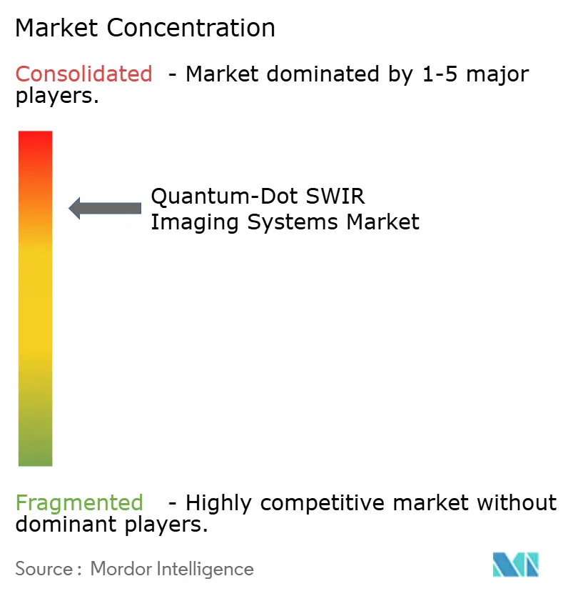
The Quantum-dot SWIR imaging systems market is consolidated at the system level and fragmented across materials and components. Teledyne Technologies, Hamamatsu Photonics, and Xenics bring established integration capabilities and customer relationships. SWIR Vision Systems, Emberion, QDI Systems, and TriEye compete through sensor cost, manufacturing compatibility, and spectral flexibility. Volume-qualified CQD deposition on 8-inch and 12-inch CMOS wafers is an important competitive capability. It is difficult to replicate because it requires coordinated development of the photodiode, ROIC, and packaging. The competitive position of each supplier, therefore, depends on both device performance and its ability to manufacture consistently at volume.
Imec demonstrated QD photodiodes integrated with metasurfaces on a 300 mm CMOS pilot line in December 2025. The licensing model could alter supplier relationships as more companies seek access to customized SWIR sensor processes. SWIR Vision Systems also disclosed a multiband focal-plane array design that combines CQD and microbolometer detection on a single ROIC. The design illustrates how intellectual property in multispectral integration can strengthen differentiation. The Quantum-dot SWIR imaging systems industry is also seeing partnerships rather than acquisitions. This reflects the specialized nature of knowledge of quantum-dot materials and the cost of integrating them into finished systems.
QDI Systems and Allied Vision announced a partnership in April 2026 to commercialize QD-based SWIR sensors for Allied Vision industrial camera platforms. The partnership targets material analysis, moisture detection, and drone imaging applications. TriEye and LITEON partnered in August 2025 on a VCSEL-powered sensing system that combines the TES200 sensor with a 1,135 nm VCSEL array. This model aligns the illumination source and receiver for automotive and industrial use. Opportunities remain in rear-view cameras, precision-agriculture drones, and consumer biometrics. No QD-SWIR supplier had achieved design-in scale in those applications across the Quantum-dot SWIR imaging systems market by mid-2026.
Quantum-Dot SWIR Imaging Systems Industry Leaders
ON Semiconductor Corporation
Emberion Oy
Qdi Systems B.V.
Quantum Solutions LLC
Nanoco Technologies Limited
- *Disclaimer: Major Players sorted in no particular order
Quantum-Dot SWIR Imaging Systems Market Companies Covered in this Report
- ON Semiconductor Corporation
- SWIR Vision Systems, Inc.
- Emberion Oy
- Qdi Systems B.V.
- Quantum Solutions LLC
- Nanoco Technologies Limited
- Teledyne Technologies Incorporated
- Teledyne FLIR LLC
- Hamamatsu Photonics K.K.
- Sony Semiconductor Solutions Corporation
- Lynred SAS
- Allied Vision Technologies GmbH
- New Imaging Technologies SA
- Raptor Photonics Limited
- Princeton Infrared Technologies, Inc.
- Sensors Unlimited, Inc.
- Xenics NV
- Corning Incorporated
- Collins Aerospace LLC
- Leonardo DRS, Inc.
- STMicroelectronics N.V.
- Interuniversitair Micro-Electronica Centrum vzw
- Qurv Technologies S.L.
- TriEye Ltd.

Recent Industry Developments in Quantum-Dot SWIR Imaging Systems Market
- May 2026: Teledyne DALSA launched Kaleido™, a SWIR hyperspectral camera delivering up to 1,280-pixel spatial resolution at line rates exceeding 2.3 kHz via a 10 GigE interface. The vertically integrated system incorporates sensor, spectrograph, and interface in a single unit targeting industrial recycling, food safety, pharmaceuticals, and waste management, significantly reducing machine-builder integration time.
- April 2026: QDI Systems B.V. and Allied Vision Technologies GmbH announced a strategic partnership to commercialize QD-based SWIR sensors as drop-in upgrades for Allied Vision's industrial camera platforms, targeting material analysis, moisture detection, and drone-based imaging markets where InGaAs cost limitations have constrained adoption.
- April 2026: DGIST, KIST, and KIMS jointly demonstrated a hybrid Ag₂Te quantum dot and MoS₂ 2D semiconductor infrared image sensor achieving 32×32 pixel array operation with stable fog and smoke imaging, targeting autonomous-vehicle applications through standard CMOS-compatible fabrication.
- April 2026: Sungkyunkwan University's team realized the world's first real-time InAs-based quantum dot infrared imager, combining a pixel array with a custom ROIC for autonomous-vehicle and security-camera applications and marking the transition from laboratory demonstrations to functional imaging systems.


Global Quantum-Dot SWIR Imaging Systems Market Report Scope
The Quantum-Dot SWIR Imaging Systems Market refers to short-wave infrared imaging solutions that utilize nanoscale semiconductor crystals (quantum dots) as their primary light-sensing material. Unlike traditional InGaAs sensors, quantum-dot detectors made from materials like lead sulfide, mercury chalcogenide, or indium arsenide offer tunable wavelength absorption, lower manufacturing costs, and easier integration with standard silicon readout circuits. These systems are increasingly adopted across industrial, automotive, food, and consumer electronics sectors for compact, cost-effective night vision, material sorting, and chemical analysis.
The Quantum-Dot SWIR Imaging Systems Market Report is Segmented by Quantum-Dot Material (Lead-Based Quantum Dots (PbS, PbSe), Mercury Chalcogenide Quantum Dots (HgTe, HgSe), Indium-Based Quantum Dots (InAs, InSb), and Other Emerging Quantum-Dot Materials), Product Type (SWIR Cameras, Camera Cores and Modules, Focal Plane Arrays and Image Sensors, and Custom/OEM Sensor Platforms), Imaging Architecture (Area-Scan Systems, Line-Scan Systems, Hyperspectral Systems, and Multispectral and Snapshot Systems), End-User Industry (Industrial Manufacturing, Semiconductor and Electronics, Aerospace and Defense, Automotive and Mobility, Food and Agriculture, Recycling and Environmental Services, Healthcare and Research Institutions, Consumer Electronics, and Other End-User Industries), and Geography (North America, South America, Europe, Asia-Pacific, and Middle East and Africa). The Market Forecasts are Provided in Terms of Value (USD).
| Lead-Based Quantum Dots (PbS, PbSe) |
| Mercury Chalcogenide Quantum Dots (HgTe, HgSe) |
| Indium-Based Quantum Dots (InAs, InSb) |
| Other Emerging Quantum-Dot Materials |
| SWIR Cameras |
| Camera Cores and Modules |
| Focal Plane Arrays and Image Sensors |
| Custom/OEM Sensor Platforms |
| Area-Scan Systems |
| Line-Scan Systems |
| Hyperspectral Systems |
| Multispectral and Snapshot Systems |
| Industrial Manufacturing |
| Semiconductor and Electronics |
| Aerospace and Defense |
| Automotive and Mobility |
| Food and Agriculture |
| Recycling and Environmental Services |
| Healthcare and Research Institutions |
| Consumer Electronics |
| Other End-User Industries |
| North America | United States | |
| Canada | ||
| Mexico | ||
| South America | Brazil | |
| Argentina | ||
| Rest of South America | ||
| Europe | Germany | |
| United Kingdom | ||
| France | ||
| Italy | ||
| Spain | ||
| Rest of Europe | ||
| Asia-Pacific | China | |
| Japan | ||
| India | ||
| South Korea | ||
| Rest of Asia-Pacific | ||
| Middle East and Africa | Middle East | Saudi Arabia |
| United Arab Emirates | ||
| Turkey | ||
| Rest of the Middle East | ||
| Africa | South Africa | |
| Nigeria | ||
| Rest of Africa | ||
| By Quantum-Dot Material | Lead-Based Quantum Dots (PbS, PbSe) | ||
| Mercury Chalcogenide Quantum Dots (HgTe, HgSe) | |||
| Indium-Based Quantum Dots (InAs, InSb) | |||
| Other Emerging Quantum-Dot Materials | |||
| By Product Type | SWIR Cameras | ||
| Camera Cores and Modules | |||
| Focal Plane Arrays and Image Sensors | |||
| Custom/OEM Sensor Platforms | |||
| By Imaging Architecture | Area-Scan Systems | ||
| Line-Scan Systems | |||
| Hyperspectral Systems | |||
| Multispectral and Snapshot Systems | |||
| By End-User Industry | Industrial Manufacturing | ||
| Semiconductor and Electronics | |||
| Aerospace and Defense | |||
| Automotive and Mobility | |||
| Food and Agriculture | |||
| Recycling and Environmental Services | |||
| Healthcare and Research Institutions | |||
| Consumer Electronics | |||
| Other End-User Industries | |||
| By Geography | North America | United States | |
| Canada | |||
| Mexico | |||
| South America | Brazil | ||
| Argentina | |||
| Rest of South America | |||
| Europe | Germany | ||
| United Kingdom | |||
| France | |||
| Italy | |||
| Spain | |||
| Rest of Europe | |||
| Asia-Pacific | China | ||
| Japan | |||
| India | |||
| South Korea | |||
| Rest of Asia-Pacific | |||
| Middle East and Africa | Middle East | Saudi Arabia | |
| United Arab Emirates | |||
| Turkey | |||
| Rest of the Middle East | |||
| Africa | South Africa | ||
| Nigeria | |||
| Rest of Africa | |||


Key Questions Answered in the Report
What is the size of the Quantum-dot SWIR imaging systems market?
The Quantum-dot SWIR imaging systems market is valued at USD 54.09 million in 2026 and is forecast to reach USD 95.88 million by 2031, at a 12.13% CAGR.
What is driving demand for quantum-dot SWIR imaging systems?
QD-on-CMOS production can lower sensor costs, while semiconductor inspection, sorting automation, and automotive sensing are expanding use cases.
Which quantum-dot material leads revenue?
Lead-based quantum dots led with 46.81% share in 2025 because of their established synthesis ecosystem and broad absorption range.
Which imaging architecture is growing fastest?
Hyperspectral systems are forecast to grow at 15.83% CAGR through 2031, supported by recycling and food-sorting applications.
Which region is expanding fastest?
Asia-Pacific is forecast to grow at 14.83% CAGR through 2031, supported by semiconductor investment in China, South Korea, and Japan.
What limits wider quantum-dot SWIR adoption?
Qualification costs, dark-current performance, temperature stability, and volume thin-film uniformity remain important constraints.
Page last updated on: