Wafer Glass Market Size and Share
Market Overview
| Study Period | 2019 - 2030 |
|---|---|
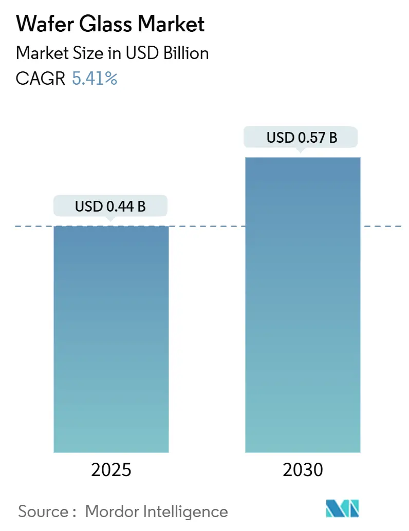
| Market Size (2025) | USD 0.44 Billion |
| Market Size (2030) | USD 0.57 Billion |
| Growth Rate (2025 - 2030) | 5.41% CAGR |
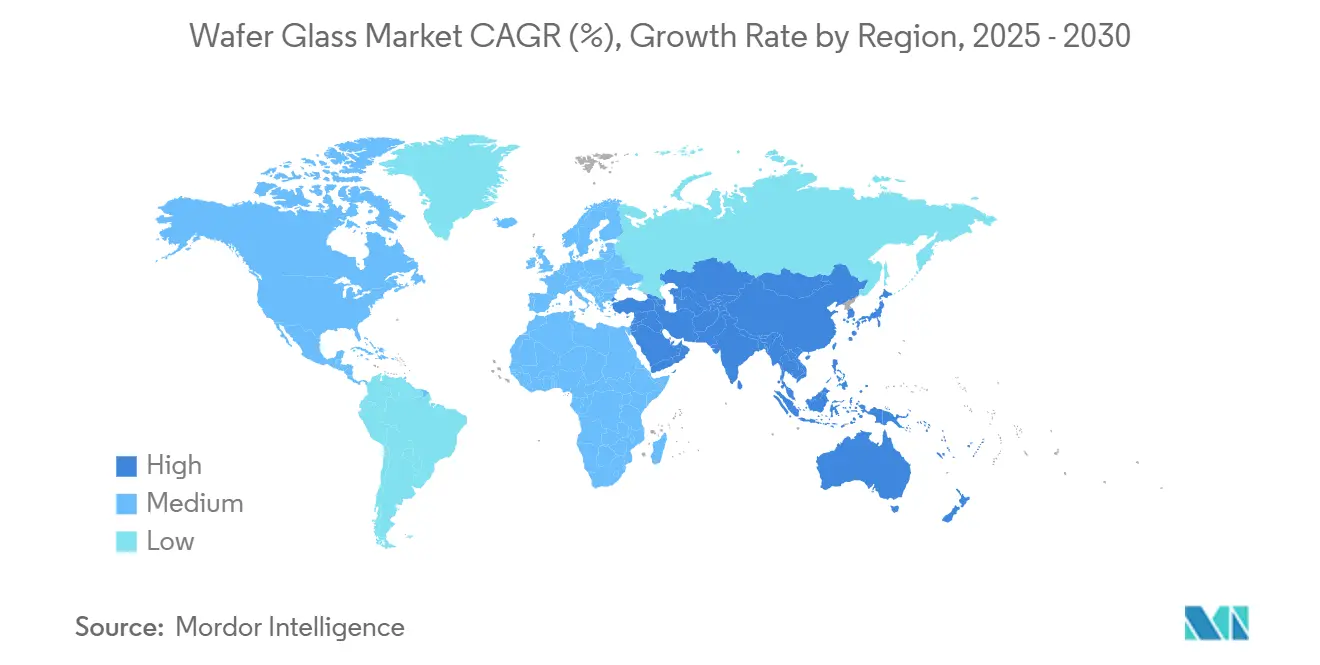
| Fastest Growing Market | Middle East |
| Largest Market | Asia Pacific |
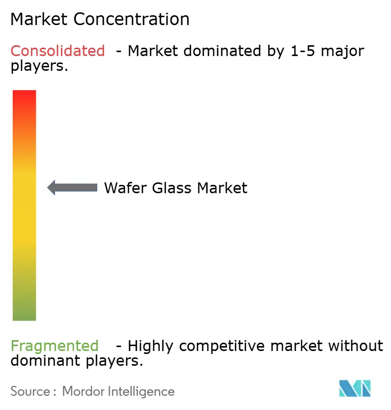
| Market Concentration | Medium |
Major Players *Disclaimer: Major Players sorted in no particular order Image © Mordor Intelligence. Reuse requires attribution under CC BY 4.0. | |
Wafer Glass Market Analysis by Mordor Intelligence
The wafer glass market size reached USD 440 million in 2025 and is projected to advance to USD 570 million by 2030, reflecting a 5.41% CAGR over the forecast period. This measured expansion stems from the accelerating adoption of through-glass vias, the widening use of these in photonic integrated circuits, and policy-driven localization incentives in North America and Europe. Intel’s 2024 decision to shift from organic laminates to glass substrates for next-generation processors signaled a structural change; however, the limited 300 mm fabrication capacity continues to constrain high-volume production. Regional stimulus programs, such as the European Union Chips Act and the U.S. CHIPS and Science Act, are unlocking new projects, but supply-chain risks tied to East Asian borosilicate refineries linger. Demand visibility is strongest in MEMS safety sensors, foldable consumer displays, and low-loss RF modules for 5G, each of which relies on the material’s hermeticity and dielectric stability. Competitive intensity remains moderate because SCHOTT, Corning, and AGC collectively control about 60% of specialty capacity, while smaller precision fabricators target niches in custom diameters and ultra-low-loss quartz wafers.
Key Report Takeaways
- By glass material type, borosilicate led with a 35.78% wafer glass market share in 2024, whereas quartz and fused silica are forecast to post the fastest 6.51% CAGR through 2030.
- By wafer diameter, 200 mm commanded 42.31% of the wafer glass market size in 2024, while 300 mm is projected to grow at a 6.27% CAGR as breakage rates decline.
- By application, MEMS and sensors accounted for 39.67% of the revenue in 2024, and photonics and optoelectronics are expected to hold the highest 6.59% forecast CAGR to 2030.
- By end-user industry, consumer electronics dominated with 43.91% of spending in 2024, whereas healthcare and biotechnology are advancing at a 6.67% CAGR on lab-on-chip demand.
- By geography, Asia-Pacific generated 53.78% of 2024 revenue, but the Middle East is set to record the quickest 6.39% CAGR on the back of Saudi Arabia’s NEOM cluster investments.
Note: Market size and forecast figures in this report are generated using Mordor Intelligence’s proprietary estimation framework, updated with the latest available data and insights as of January 2026.
Global Wafer Glass Market Trends and Insights
Drivers Impact Analysis*
| Driver | (~) % Impact on CAGR Forecast | Geographic Relevance | Impact Timeline |
|---|---|---|---|
| Surge in through-glass via adoption for high-density 3D packaging | +1.2% | Taiwan, South Korea, United States | Medium term (2-4 years) |
| Growing demand from MEMS sensors in automotive safety systems | +0.9% | North America, Europe, China | Short term (≤ 2 years) |
| Expansion of 5G and RF front-end modules requiring low-loss glass interposers | +0.8% | China, South Korea, Japan, United States | Medium term (2-4 years) |
| Ultra-thin flexible glass enabling foldable and wearable electronics | +0.7% | South Korea, China, United States | Short term (≤ 2 years) |
| Emergence of glass-based photonic integrated circuits for AI accelerators | +1.0% | United States, Europe | Long term (≥ 4 years) |
| Localization incentives for semiconductor material supply chains | +0.6% | United States, Canada, Germany, Netherlands, France | Long term (≥ 4 years) |
| Source: Mordor Intelligence | |||
Surge in Through-Glass Via Adoption for High-Density 3D Packaging
Through-glass vias are redefining heterogeneous integration by supporting vertical interconnect pitches of less than 10 µm, a density that organic build-up substrates cannot match.[1]Intel Corporation, “Intel Unveils Glass Substrates for Next-Gen Advanced Packaging,” intel.com Intel’s 2024 roadmap targets a 50% drop in signal loss and a tenfold rise in interconnect density, validating glass as the preferred medium for future chiplet architectures. Taiwanese pilot lines have begun small-lot qualification, while U.S. laser-drilling specialist LPKF demonstrated 5 µm vias with less than 2% taper, lowering parasitic capacitance by 30% relative to silicon interposers. Automotive and aerospace labs reported borosilicate structures that survived 1,000 temperature cycles between −40 °C and 125 °C without delamination, answering reliability concerns. As a result, adoption momentum is likely to accelerate once 300 mm capacity constraints ease.
Growing Demand from MEMS Sensors in Automotive Safety Systems
Mandatory advanced driver-assistance features in Europe, China, and the United States have expanded per-vehicle MEMS sensor counts, propelling demand for glass cap wafers that ensure hermetic sealing. Bosch disclosed an 18% increase in shipments for 2024, citing glass packages that reduce moisture ingress and drift by 40% over 10 years compared to ceramic lids.[2]Bosch Sensortec, “Automotive MEMS Sensor Growth,” bosch.com STMicroelectronics achieved a 30% height reduction in inertial units by switching to wafer-level glass caps, enabling slimmer steering column assemblies. Chinese mandates stipulating at least 12 MEMS sensors in each new energy vehicle by 2025 are further stimulating regional capacity adds, even though sub-500 µm thinning still faces yield penalties.
Expansion of 5G and RF Front-End Modules Requiring Low-Loss Glass Interposers
Millimeter-wave radios demand insertion loss below 0.5 dB, a threshold that conventional laminates struggle to meet. A 2024 MDPI study showed that laminated glass substrates reached a 0.3 dB loss at 28 GHz, while trimming module costs were reduced by 25%, outclassing low-temperature co-fired ceramics.[3]MDPI, “Laminated Glass Substrates for 5G RF Modules,” mdpi.com Qualcomm’s Snapdragon X80 modem utilizes glass interposers for its antenna-tuning networks, underscoring the material’s value at the handset scale. Korea’s Ministry of Science and ICT earmarked USD 37.5 million in 2024 for quartz wafer R&D, and AGC noted a 60% order surge for alkaline-free glass destined for RF power amplifiers.
Ultra-Thin Flexible Glass Enabling Foldable and Wearable Electronics
Consumer electronics brands have validated 30 µm glass as a cover-lens solution for foldable smartphones, achieving bending radii of less than 1.5 mm and durability exceeding 200,000 folding cycles. Ultra-thin glass also supports curved wearable displays and hearable acoustics modules, where hermetic encapsulation suppresses corrosion from sweat. Rapid progress in ion-exchange strengthening techniques has increased flexural strength, yet process windows remain tight, limiting supply to a handful of Asian lines. These advances underpin continued premium pricing, reinforcing the material’s strategic role in next-generation devices.
Restraints Impact Analysis*
| Restraint | (~) % Impact on CAGR Forecast | Geographic Relevance | Impact Timeline |
|---|---|---|---|
| High processing fragility and wafer breakage rates in sub-200 µm glass | -0.8% | Taiwan, South Korea, United States | Short term (≤ 2 years) |
| Limited availability of 300 mm glass wafer fabrication lines | -0.6% | Global bottlenecks, notably North America and Europe | Medium term (2-4 years) |
| Thermal expansion mismatch challenges in heterogeneous integration | -0.4% | United States, Europe, Asia-Pacific hubs | Medium term (2-4 years) |
| Geopolitical concentration of borosilicate supply chain in East Asia | -0.3% | Dependent regions worldwide | Long term (≥ 4 years) |
| Source: Mordor Intelligence | |||
High Processing Fragility and Wafer Breakage Rates in Sub-200 µm Glass
Industry monitoring reveals breakage rates exceeding 15% during dicing and bonding for wafers thinner than 200 µm, resulting in scrap costs of up to USD 18 per 200 mm wafer. Edge chipping during laser singulation contributes 60% of failures, prompting suppliers to develop chemically strengthened aluminosilicate grades with 40% higher flexural strength, albeit at a 30% price premium. Plan Optik’s 2024 quality data revealed a 22% rise in cracked-wafer returns, driving investment in automated inspection and reinforced carriers. Corning ultimately paused the development of ultra-thin Gorilla Glass for semiconductor packaging because ion-exchange steps conflict with ±2 µm thickness tolerances, underscoring the complexity of closing the breakage gap.
Limited Availability of 300 mm Glass Wafer Fabrication Lines
Fewer than five commercial fabs can deliver 300 mm glass wafers at semiconductor tolerances, leaving global capacity at less than 50,000 wafers per month, compared to more than 7 million for silicon. Intel’s USD 8.5 billion Arizona expansion will pilot 300 mm production in late 2026, but initial output is earmarked for internal needs. Foundry majors in Taiwan and South Korea evaluated glass interposers in 2024, but deferred volume commitments due to supplier diversity remaining thin and lead times exceeding 24 weeks. Absent standardized specifications, each customer requests bespoke thicknesses and thermal-expansion bands, diluting scale economies and prolonging tool qualification cycles.
*Our forecasts treat driver/restraint impacts as directional, not additive. The impact forecasts reflect baseline growth, mix effects, and variable interactions.
Segment Analysis
By Glass Material Type: Borosilicate Retains Leadership as Quartz Gains Pace
Borosilicate accounted for 35.78% of 2024 revenue, reflecting its coefficient of thermal expansion matching that of silicon, which simplifies MEMS encapsulation and sensor packaging. The wafer glass market size tied to borosilicate is projected to expand steadily as automotive and industrial OEMs favor its established supply chain. Quartz and fused silica, however, are poised to accelerate at a 6.51% CAGR to 2030, buoyed by photonic integrated circuit designs that require ultra-low dielectric loss and index stability across 1,260 nm to 1,360 nm wavelengths. Alkaline-free glass, originally qualified for TFT-LCD backplanes, is transitioning into OLED substrates, where alkali ion migration can degrade pixel life. Both Corning and AGC ramped up additional lines in 2024 to serve flexible displays. Aluminosilicate occupies a premium niche for implantable sensors and aerospace transducers, thanks to its 40% higher flexural strength. However, its 20%–30% cost premium tempers its broader appeal. Soda-lime persists mainly as a low-precision carrier material in microfluidics.
Second-order momentum centers on Intel’s call for borosilicate grades with thermal expansion below 3.5 ppm/K to curb warpage on chiplet panels larger than 50 mm × 50 mm. Co-packaged optics amplifies quartz demand because embedded waveguides require a refractive-index variance of less than 0.001, a tolerance that only fused silica achieves reliably. Specialty formulations, such as phosphate or chalcogenide glass, represent less than 5% of the value but are finding traction in bioactive microfluidic coatings and infrared optics, thereby widening the wafer glass market footprint in life-science instrumentation. Collectively, these trends indicate that material portfolios will diversify even as borosilicate remains the industry workhorse.


By Wafer Diameter: 200 mm Dominates, While 300 mm Plots a Gradual Ascent
The 200 mm node captured 42.31% of the wafer glass market share in 2024, aligning with the installed base of MEMS and RF front-end lines that favor mature tooling and well-understood handling protocols. Although 200 mm substrates continue to underpin consumer, industrial, and automotive sensor output, the 300 mm format is forecast to record a 6.27% CAGR, contingent on conquering sub-200 µm breakage and expanding usable capacity beyond pilot lines. Standards ratified by SEMI in 2024 set flatness limits at ±2 µm for 300 mm wafers, a threshold presently met by fewer than five suppliers worldwide, underscoring the technical hurdle.
Migration from 200 mm to 300 mm promises die-per-wafer cost benefits and higher yield for large-area interposers but imposes an 18- to 24-month requalification cycle for adhesives, dicing, and metrology. Foundries evaluating high-bandwidth-memory glass interposers disclosed postponements to 2026, echoing the supply shortfall. Legacy 150 mm lines remain relevant in automotive radar filters and microfluidic chips that require smaller die footprints with lower capital intensity; Plan Optik logged a 12% rise in 150 mm orders in 2024, tied to radar module demand. Niche 100 mm and custom diameters, such as 125 mm, linger for prototype, aerospace, or specialty sensor production, where volumes remain insufficient to justify dedicated automation.
By Application: MEMS Leads, Photonics Surges
MEMS and sensors accounted for 39.67% of the 2024 value, capitalizing on glass’s moisture barrier, optical clarity, and coefficient of thermal expansion alignment with silicon. Regulatory safety mandates in Europe and China underpin sustained growth in MEMS units, translating into stable demand for borosilicate caps. The photonics and optoelectronics segment is expected to accelerate at a 6.59% CAGR through 2030 as hyperscale data centers adopt co-packaged optics, driving up fused silica wafer usage. Advanced semiconductor packaging, which encompasses through-glass vias and large-panel interposers, expanded by 14% in 2024, driven by Intel and TSMC pilot programs. However, a rapid ramp-up depends on the availability of a 300 mm supply.
Wafer-level packaging and carrier substrates leveraged for fan-out processes are growing as 5G smartphones and wearables demand sub-0.4 mm package heights. Microfluidics and biochips remain a high-growth niche because optical detection and chemical inertness drive the selection of glass over polymer. Dolomite Microfluidics doubled shipments of point-of-care diagnostic chips in 2024, emblematic of healthcare’s rising share. Emerging hybrid applications, such as LiDAR scanning mirrors that integrate MEMS and photonics, demonstrate the expanding scope of glass substrates in cross-disciplinary device architectures.

By End-User Industry: Consumer Electronics Dominates, Healthcare Gains Velocity
Consumer electronics accounted for 43.91% of 2024 revenue, driven by ultra-thin glass in foldable smartphones, curved wearables, and true wireless earbuds. Samsung’s 2024 launches showcased 30 µm cover lenses that deliver scratch resistance equivalent to Mohs hardness 6 while enabling fold radii below 1.5 mm. Automotive adoption is intensifying as driver-assistance mandates boost glass-capped sensor requirements; each European passenger vehicle now integrates multiple pressure, inertial, and radar modules sealed within a glass enclosure. Industrial and manufacturing users rely on glass for pressure sensors exposed to corrosive media or temperatures surpassing 200 °C, with Honeywell confirming qualification in chemical plants.
Healthcare and biotechnology are forecast to post a 6.67% CAGR, propelled by lab-on-chip diagnostics, implantable glucose monitors, and surgical navigation devices that exploit glass’s biocompatibility and optical clarity. Aerospace and defense industries leverage radiation-hardened glass wafers for satellite attitude control units and missile guidance, thereby reducing weight and cost compared to fiber-optic gyros. Telecommunications infrastructure and energy management systems complete the roster, utilizing low-loss interposers to route RF signals in 5G base stations and grid sensors. Collectively, the expansion of healthcare and industrial niches complements the dominant electronics base, cushioning the cyclicality in consumer demand.
Geography Analysis
Asia-Pacific accounted for 53.78% of 2024 revenue, underpinned by Taiwan’s fan-out wafer-level packaging capacity, Japan’s precision grinding leadership, and China’s MEMS sensor expansion. Taiwanese lines in Hsinchu and Tainan deliver the bulk of global redistribution layer processing, relying on glass carriers to handle ultra-thin dies. Nippon Electric Glass and AGC together produce more than 40% of the worldwide borosilicate wafers, benefiting from decades of LCD substrate expertise that yields flatness of ≤1 µm on 200 mm diameter wafers. South Korea earmarked USD 37.5 million for quartz wafer R&D in 2024, reflecting public-private intent to reduce reliance on Japanese inputs. Chinese policy classified glass substrates as strategic, prompting BOE and the Tunghsu Group to pilot lines for 200 mm OLED encapsulation and MEMS caps. India and Australia remain nascent but position glass for defense and mining-automation sensors.
The Middle East and Africa are projected to grow at a 6.39% CAGR through 2030 as Saudi Arabia channels USD 1.2 billion into its NEOM semiconductor hub and the United Arab Emirates expands GlobalFoundries capacity, including prospective glass interposer lines. Egypt and South Africa continue to rely on imports, serving primarily academic and pilot needs. North America captured 18% of 2024 turnover, buoyed by the U.S. CHIPS and Science Act’s USD 39 billion incentives that backed Intel’s Arizona pilot and attracted European suppliers exploring U.S. fabs. Canada’s demand is concentrated in the aerospace sector, while Mexico consumes glass carriers in assembly and testing.
Europe contributed roughly 15% of 2024 revenue, led by Germany, France, and the Netherlands, which drew on automotive MEMS and photonics R&D. Ephos secured EUR 41.5 million (USD 44.4 million) to build a glass photonics pilot in the Netherlands, aligning with the EUR 43 billion (USD 46 billion) Chips Act. STMicroelectronics’ EUR 5 billion (USD 5.35 billion) Italian expansion will integrate glass interposers for automotive radar by 2026. Germany’s Fraunhofer Institute published mitigation paths for thermal-expansion mismatch, highlighting polymer buffers as a near-term remedy. The United Kingdom and France focus on defense applications, whereas Russia faces restrictions on importing tools. South America remains under 3% share, relying on imports for automotive and medical prototypes.

Competitive Landscape
The wafer glass market exhibits moderate concentration, with SCHOTT, Corning, and AGC accounting for approximately 60% of specialty capacity. However, custom geometries and ultra-low-loss quartz remain fragmented. SCHOTT’s 2023 acquisition of Hoya’s semiconductor glass assets broadened access to MEMS caps and photonic wafers, leveraging its ophthalmic expertise for sub-1 µm surface roughness. Corning focuses on display-grade and photonics substrates after pausing ultra-thin Gorilla Glass for packaging due to tolerance conflicts. AGC scaled alkaline-free lines to serve flexible OLED producers and telecom RF modules, lifting 2025 shipment guidance.
Second-tier suppliers, including Plan Optik and TECNISCO, differentiate themselves through rapid prototyping, non-standard diameters, and etched cavity wafers for biomedical applications; Plan Optik recorded a 22% increase in custom orders in 2024. Emerging player Ephos targets glass-based photonic integrated circuits, with EUR 41.5 million funding to challenge incumbent silicon photonics suppliers by embedding lasers directly in glass. The technology race centers on through-glass via yield, where LPKF’s laser microvia process achieves 5 µm diameters with a 2% taper, potentially enabling orders-of-magnitude higher interconnect density. Intel’s vertical integration could alter supply balances if excess 300 mm output is commercialized post-2027. Capital barriers exceeding USD 100 million per greenfield fab, combined with concentrated process know-how, temper the velocity of new entrants and support moderate margins.
Wafer Glass Industry Leaders
SCHOTT AG
Corning Incorporated
AGC Inc.
Nippon Electric Glass Co., Ltd.
Plan Optik AG
- *Disclaimer: Major Players sorted in no particular order

Recent Industry Developments
- November 2025: Intel completed tooling installation at its Arizona glass substrate pilot line and began engineering-lot runs of 300 mm wafers, targeting qualification for advanced packaging flows by mid-2026.
- August 2025: Ephos secured EUR 41.5 million (USD 44.4 million) in European Chips Act funding to build a Dutch pilot facility for glass-based photonic integrated circuits aimed at hyperscale data centers.
- May 2025: Corning and Applied Materials launched a USD 120 million joint R and D initiative in New York to develop an ion-exchange-free strengthening process for 300 mm glass substrates, with pilot output scheduled for 2027.
- February 2025: SCHOTT inaugurated a dedicated 200 mm aluminosilicate glass wafer line in Mainz, Germany, expanding annual capacity by 180,000 wafers to support implantable medical sensor programs.


Global Wafer Glass Market Report Scope
The Wafer Glass Market Report is Segmented by Glass Material Type (Borosilicate, Quartz/Fused Silica, Alkaline-Free, Aluminosilicate, Soda-Lime, Other Glass Material Type), Wafer Diameter (100 mm, 150 mm, 200 mm, 300 mm, Other Wafer Diameter), Application (MEMS and Sensors, Advanced Semiconductor Packaging, Wafer-Level Packaging, Microfluidics and Biochips, Photonics and Optoelectronics, Other Application), End-User Industry (Consumer Electronics, Automotive, Industrial and Manufacturing, Healthcare and Biotechnology, Aerospace and Defense, Other End-User Industry), and Geography (North America, Europe, Asia-Pacific, Middle East and Africa, South America). The Market Forecasts are Provided in Terms of Value (USD).
| Borosilicate Glass |
| Quartz / Fused Silica |
| Alkaline-Free Glass |
| Aluminosilicate Glass |
| Soda-Lime Glass |
| Other Glass Material Type |
| 100 mm |
| 150 mm |
| 200 mm |
| 300 mm |
| Other Wafer Diameter |
| MEMS and Sensors |
| Advanced Semiconductor Packaging (TGV, Interposers) |
| Wafer-Level Packaging / Carrier Substrates |
| Microfluidics and Biochips |
| Photonics and Optoelectronics |
| Other Application |
| Consumer Electronics |
| Automotive |
| Industrial and Manufacturing |
| Healthcare and Biotechnology |
| Aerospace and Defense |
| Other End-User Industry |
| North America | United States | |
| Canada | ||
| Mexico | ||
| Europe | Germany | |
| United Kingdom | ||
| France | ||
| Russia | ||
| Rest of Europe | ||
| Asia-Pacific | China | |
| Japan | ||
| India | ||
| South Korea | ||
| Australia | ||
| Rest of Asia-Pacific | ||
| Middle East and Africa | Middle East | Saudi Arabia |
| United Arab Emirates | ||
| Rest of Middle East | ||
| Africa | South Africa | |
| Egypt | ||
| Rest of Africa | ||
| South America | Brazil | |
| Argentina | ||
| Rest of South America | ||
| By Glass Material Type | Borosilicate Glass | ||
| Quartz / Fused Silica | |||
| Alkaline-Free Glass | |||
| Aluminosilicate Glass | |||
| Soda-Lime Glass | |||
| Other Glass Material Type | |||
| By Wafer Diameter | 100 mm | ||
| 150 mm | |||
| 200 mm | |||
| 300 mm | |||
| Other Wafer Diameter | |||
| By Application | MEMS and Sensors | ||
| Advanced Semiconductor Packaging (TGV, Interposers) | |||
| Wafer-Level Packaging / Carrier Substrates | |||
| Microfluidics and Biochips | |||
| Photonics and Optoelectronics | |||
| Other Application | |||
| By End-User Industry | Consumer Electronics | ||
| Automotive | |||
| Industrial and Manufacturing | |||
| Healthcare and Biotechnology | |||
| Aerospace and Defense | |||
| Other End-User Industry | |||
| By Geography | North America | United States | |
| Canada | |||
| Mexico | |||
| Europe | Germany | ||
| United Kingdom | |||
| France | |||
| Russia | |||
| Rest of Europe | |||
| Asia-Pacific | China | ||
| Japan | |||
| India | |||
| South Korea | |||
| Australia | |||
| Rest of Asia-Pacific | |||
| Middle East and Africa | Middle East | Saudi Arabia | |
| United Arab Emirates | |||
| Rest of Middle East | |||
| Africa | South Africa | ||
| Egypt | |||
| Rest of Africa | |||
| South America | Brazil | ||
| Argentina | |||
| Rest of South America | |||


Key Questions Answered in the Report
How large is the wafer glass market in 2025 and what growth is expected by 2030?
The wafer glass market size reached USD 440 million in 2025 and is forecast to rise to USD 570 million by 2030, reflecting a 5.41% CAGR.
Which glass material type currently dominates commercial demand?
Borosilicate glass leads with a 35.78% share because its thermal expansion matches silicon, simplifying MEMS and sensor packaging.
What applications will drive the fastest revenue growth through 2030?
Photonics and optoelectronics are projected to record the highest 6.59% CAGR as data centers adopt co-packaged optics on glass substrates.
Why is 300 mm adoption slower than 200 mm in glass wafers?
Fewer than five fabs worldwide can deliver 300 mm glass wafers at semiconductor tolerances, and sub-200 µm breakage rates exceed 15%, slowing ramp-up.
Which region holds the biggest share and which is growing fastest?
Asia-Pacific held 53.78% of 2024 revenue, while the Middle East is forecast to grow at the quickest 6.39% CAGR driven by Saudi and UAE investments.
Who are the leading suppliers of specialty glass wafers today?
SCHOTT, Corning, and AGC collectively control about 60% of global specialty wafer capacity, with Plan Optik and TECNISCO serving custom niches.
Page last updated on:


