United States Printed Circuit Board Market Size and Share
Market Overview
| Study Period | 2020 - 2031 |
|---|---|
| Forecast Data Period | 2026 - 2031 |
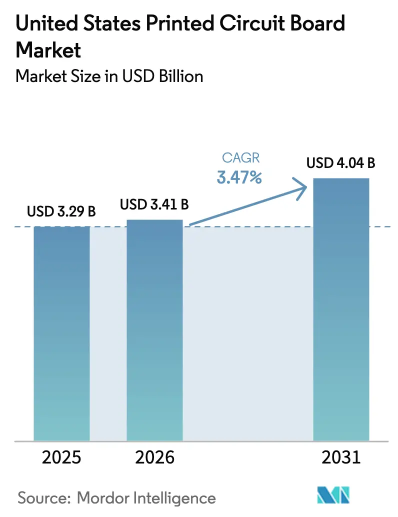
| Base Year Market Size (2025) | USD 3.29 Billion |
| Market Size (2026) | USD 3.41 Billion |
| Market Size (2031) | USD 4.04 Billion |
| Growth Rate (2026 - 2031) | 3.47% CAGR |
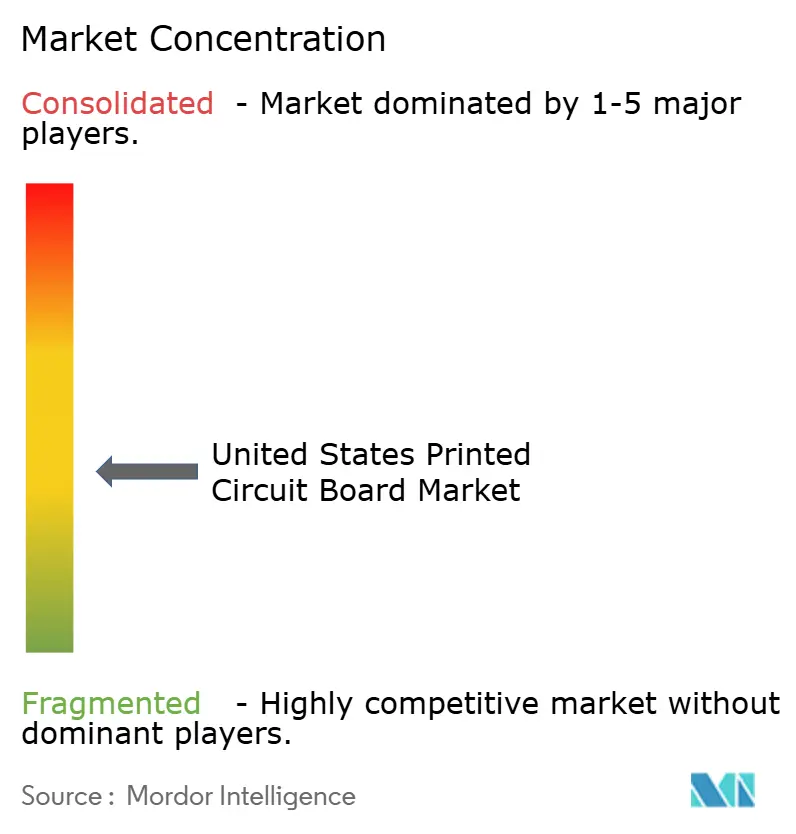
| Market Concentration | Medium |
Major Players *Disclaimer: Major Players sorted in no particular order Image © Mordor Intelligence. Reuse requires attribution under CC BY 4.0. | |
United States Printed Circuit Board Market Analysis by Mordor Intelligence
The United States Printed Circuit Board Market size in 2026 is estimated at USD 3.41 billion, growing from 2025 value of USD 3.29 billion with projections showing USD 4.04 billion, growing at 3.47% CAGR over 2026-2031. This expansion is fueled by federal onshoring incentives, escalating demand for security-cleared electronics, and a shift toward high-value substrates for advanced packaging. Federal funding under the CHIPS and Science Act has unlocked USD 3 billion for the National Advanced Packaging Manufacturing Program, accelerating investments in IC substrates and HDI boards. Parallel defense procurement rules now require ITAR-compliant supply chains, redirecting aerospace and military orders to vetted domestic fabricators. Flexible circuits are set to outpace the overall United States PCB market as wearable health devices, foldable phones, and automotive sensor arrays demand bendable interconnects. Meanwhile, hyperscale data centers are migrating to low-loss laminates that minimize signal attenuation on 800G and 1.6T switch backplanes, pushing material suppliers to expand high-speed resin capacity. Competitive intensity is moderate because the five largest fabricators account for only 40% of revenue, leaving space for regional specialists to thrive.
Key Report Takeaways
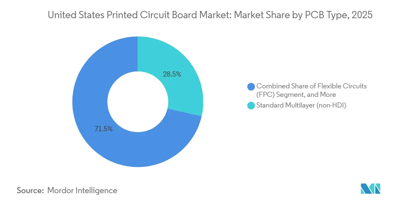
- By PCB type, standard multilayer PCBs held 28.54% revenue share in 2025, while flexible circuits are projected to expand at a 4.11% CAGR through 2031.
- By substrate material, glass epoxy FR-4 captured 44.39% of the United States printed circuit board market in 2025; high-speed, low-loss laminates are advancing at a 4.71% CAGR through 2031.
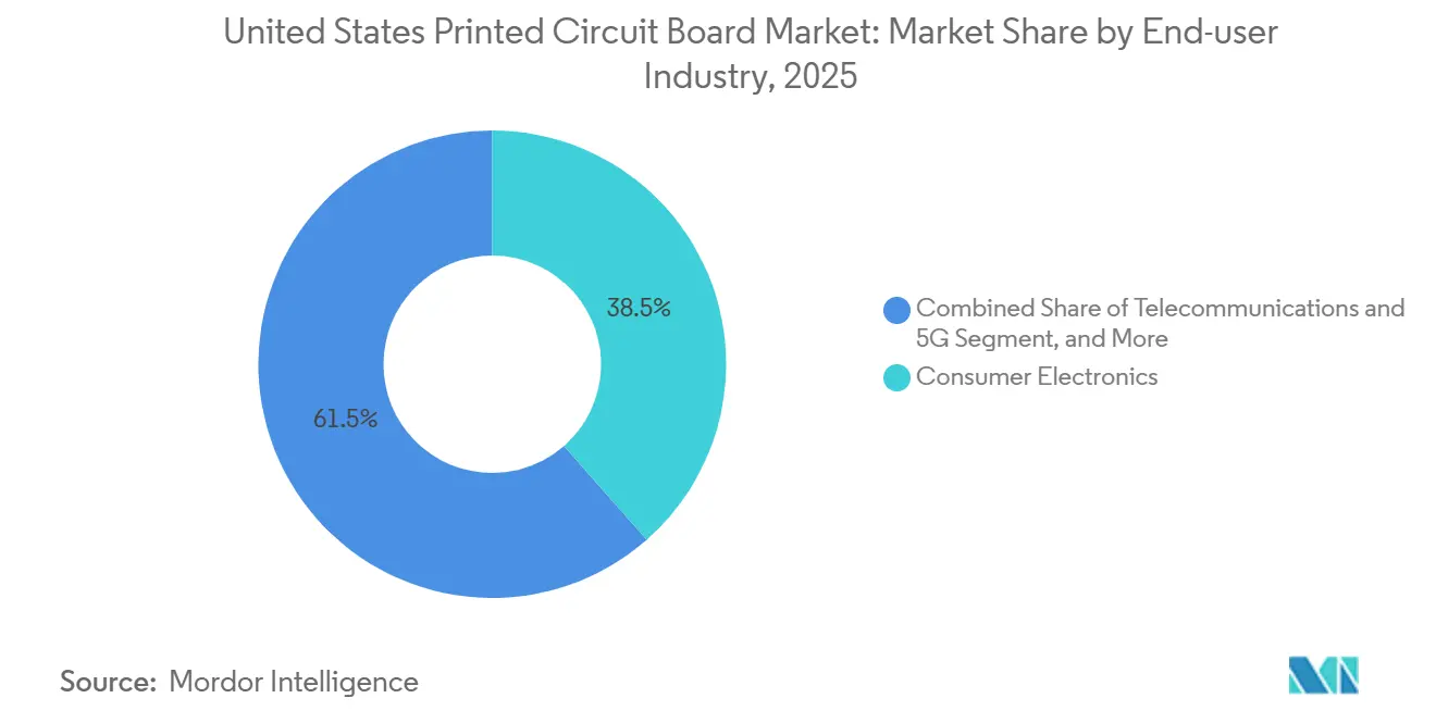
- By end-user industry, consumer electronics accounted for 38.53% of the United States PCB market share in 2025, while telecommunications and 5G infrastructure are forecast to grow at a 4.64% CAGR through 2031.
Note: Market size and forecast figures in this report are generated using Mordor Intelligence’s proprietary estimation framework, updated with the latest available data and insights as of January 2026.
United States Printed Circuit Board Market Trends and Insights
Drivers Impact Analysis*
| Driver | (~) % Impact on CAGR Forecast | Geographic Relevance | Impact Timeline |
|---|---|---|---|
| Rising Demand for IC Substrates in Advanced Packaging | +0.9% | Arizona, Ohio, Texas semiconductor corridors | Medium term (2-4 years) |
| Onshoring Incentives Under the CHIPS and Science Act | +0.8% | Nationwide semiconductor clusters | Medium term (2-4 years) |
| Growing Adoption of HDI Boards in 5G Infrastructure | +0.7% | Metropolitan and rural broadband zones | Short term (≤ 2 years) |
| Increasing Miniaturization in Consumer Electronics | +0.6% | Coastal innovation hubs | Long term (≥ 4 years) |
| Growth of Electric Vehicles Requiring High-Reliability Rigid-Flex | +0.5% | Michigan, Tennessee, California | Long term (≥ 4 years) |
| Emergence of Defense-Specific Security-Cleared Supply Chains | +0.4% | Virginia, California, Texas | Medium term (2-4 years) |
| Source: Mordor Intelligence | |||
Rising Demand for IC Substrates in Advanced Packaging
Intel is building advanced packaging capacity in Arizona and Ohio, creating a domestic pull for package substrates that previously flowed offshore. [1]Intel Corporation, “Advanced Packaging Technology,” intel.com The company’s Foveros and EMIB architectures require trace widths below 10 μm, prompting TTM Technologies and peers to retrofit lines with laser direct imaging and modified semi-additive processes. Grants that cover 35% of equipment costs under the National Advanced Packaging Manufacturing Program reduce payback risk and have shortened investment lead times to under two years. Once qualified, these ultra-fine-pitch lines deliver gross margins above 30%, making substrates the most profitable slice of the United States PCB market. Fabricators able to master sub-10-μm lithography and low-warpage materials will capture a disproportionate share of value as assembly operations repatriate.
Onshoring Incentives Under the CHIPS and Science Act
The CHIPS and Science Act provides USD 39 billion in fabrication subsidies and requires beneficiaries to source 55% of their inputs domestically, including PCBs. TSMC’s Arizona fab has already pre-qualified three United States PCB market suppliers for advanced-packaging test vehicles, a stark pivot from its Taiwan-centric supply chain. Federal workforce programs within the National Semiconductor Technology Center are training technicians in sequential lamination and automated optical inspection, easing the labor bottleneck. [2]National Science Foundation, “National Semiconductor Technology Center,” nsf.gov Concentrated clusters in Arizona, Ohio, and Texas now nurture co-located laminators, drill shops, and chemical suppliers, lowering logistics costs and trimming lead times from weeks to days. The result is a reinforcing loop that makes geographic proximity a competitive advantage.
Growing Adoption of HDI Boards in 5G Infrastructure
Open RAN base stations route multi-gigabit SerDes signals across blind and buried vias, turning HDI boards into gating components for 5G rollout. [3]Federal Communications Commission, “5G Fund for Rural America,” fcc.gov The FCC’s 5G Fund for Rural America distributed USD 9 billion during 2024-2025 and compels awardees to use trusted vendors. Verizon and AT&T have since signed multi-year HDI supply agreements with domestic fabricators, departing from prior Asia-centric sourcing. Commercial success hinges on achieving 3-mil traces and 8-mil vias while sustaining yields above 85%, a spec that demands inline optical inspection and real-time process control. Early movers who invested in sequential lamination presses between 2024-2025 are now capturing price premiums and locking in capacity reservations.
Increasing Miniaturization in Consumer Electronics
Wearable health monitors and foldable smartphones require flexible circuits with component densities exceeding 200 parts per square inch. Apple validated rigid-flex at scale in its latest smartwatch, blending battery management, wireless charging, and biometric sensing on a single folded assembly. Second-tier OEMs are following suit, seeking United States PCB market partners with expertise in polyimide laminates and stiffener bonding. Medical device makers value FDA-registered facilities and lot traceability, adding another layer of domestic pull. Engineering complexity stretches design cycles, enabling fabricators that provide co-development support to win stickier, higher-margin business over low-cost competitors.
Restraints Impact Analysis*
| Restraint | (~) % Impact on CAGR Forecast | Geographic Relevance | Impact Timeline |
|---|---|---|---|
| Volatility in Copper and Resin Prices | -0.5% | Nationwide commodity exposure | Short term (≤ 2 years) |
| Capital-Intensive Nature of Advanced PCB Fabrication | -0.4% | Mid-tier fabricators across United States | Medium term (2-4 years) |
| Limited Domestic HDI Capacity Versus Asia-Pacific Suppliers | -0.3% | High-volume HDI hubs | Medium term (2-4 years) |
| Stringent Environmental Compliance Costs | -0.2% | California, New York, Massachusetts | Long term (≥ 4 years) |
| Source: Mordor Intelligence | |||
Volatility in Copper and Resin Prices
Copper foil, which accounts for roughly 18% of PCB material costs, swung by 35% between January 2024 and December 2025 due to South American mine disruptions and speculative trading on the London Metal Exchange. Fabricators holding fixed-price contracts absorbed the spike, compressing gross margins by up to 300 basis points. Those with pass-through clauses faced customer resistance and lost bids to Asian rivals willing to lock in lower prices. Epoxy resin shocks compounded the pain when a Taiwanese supplier idled capacity for environmental upgrades, forcing North American laminators to import at a 20% premium. Larger incumbents negotiated long-term caps with copper mills, but smaller shops shifted to cost-plus quoting, trading competitiveness for cash-flow stability. Such swings accelerate consolidation because mid-tier firms lack the scale to hedge effectively.
Capital-Intensive Nature of Advanced PCB Fabrication
Laser drilling, sequential lamination, and automated inspection push a single HDI line past USD 50 million, with payback periods extending beyond 5 years. [4]Semiconductor Equipment and Materials International, “HDI Equipment Cost,” semi.org Private-equity-backed firms eyeing three-year exits often bypass these projects, while family-owned shops struggle to secure bank financing. Early adopters now face obsolescence as CO₂ lasers cede ground to UV systems, triggering a second capex cycle. The CHIPS Act grants an offset of up to 35% of equipment costs, yet the application is compliance-heavy and offers only cash reimbursement, placing the liquidity burden on applicants. The outcome is a bifurcated market that locks most regional specialists into prototypes and low-layer-count boards, relegating the volume HDI tier to a handful of well-capitalized players.
*Our forecasts treat driver/restraint impacts as directional, not additive. The impact forecasts reflect baseline growth, mix effects, and variable interactions.
Segment Analysis
By PCB Type: Flexible Circuits Lead Innovation Wave
Standard multilayer boards accounted for 28.54% of revenue in 2025, thanks to entrenched demand in industrial controls, LED lighting, and legacy computing platforms, where cost stability outweighs miniaturization. The United States printed circuit board market for rigid-flex is growing rapidly, but volume remains modest relative to commodity multilayer volumes. High-density interconnect boards, essential for 5G radios and data-center switches, face domestic capacity constraints that force some OEMs to dual-source offshore despite security concerns. At the low end, rigid 1-2-sided boards serve power supplies and simple control circuits, a segment in gentle decline as functions consolidate onto multilayers. Flexible circuits are forecast to grow at a 4.11% CAGR through 2031, doubling the pace of the overall United States PCB market. These polyimide-based boards bend around batteries, hinge assemblies, and curved housings where rigid laminates cannot fit. Rigid-flex designs command a 30%-50% price premium yet slash assembly steps and connector count, boosting reliability in wearables and implantables.
Domestic substrates for flip-chip and 2.5D interposers reach pricing above USD 50 per unit, making IC substrates the most lucrative category on a per-square-inch basis. Fabricators honing sub-10-μm features and flat-warpage laminations are building multi-year order books underwritten by CHIPS Act grants. Metal-core boards for LED thermal management, ceramic substrates for high-power microwave amplifiers, and heavy-copper boards for industrial drives fill specialized niches where performance demands preclude FR-4 substitution. Although they account for only a mid-single-digit share, these specialty formats carry margins that can exceed 35%, cushioning firms against price compression in commodity multilayers.


By Substrate Material: High-Speed Laminates Capture Data-Center Spend
Glass epoxy FR-4 accounted for 44.39% of material revenue in 2025 and will retain the top spot by volume, as it balances cost, mechanical strength, and process familiarity. Yet hyperscale data-center operators are ramping 800G and 1.6T Ethernet fabrics that require dielectric loss tangents below 0.002 at 10 GHz. To meet the spec, buyers are shifting toward low-loss laminates such as Rogers RO4000 and Isola I-Speed, which are price three to five times higher but enable longer copper runs without retimers. The United States printed circuit board market demand for these premium resins is growing at a 4.71% CAGR through 2031. Polyimide remains the substrate of choice for both flexible and rigid-flex constructions because its 260 °C glass transition temperature withstands lead-free reflow and aerospace thermal cycles. Packaging resins like Ajinomoto build-up film are designed for IC substrates that must match the coefficient of thermal expansion of silicon, tightening tolerances to the single-digit ppm level.
Metal-core laminates continue to serve LED lighting, while ceramic and aluminum-nitride boards dominate high-frequency radar and power electronics. Although volumes are small, these materials enable United States PCB market suppliers to diversify into defense and electric vehicle traction inverters, both of which pay premiums for reliability. Composite epoxy materials blend resin systems to reduce costs while preserving mid-tier electrical performance, appealing to consumer devices that need moderate-loss budgets at mass-market pricing. Collectively, the gradual shift toward sophisticated laminates offsets flat-to-declining volumes in commodity FR-4, supporting revenue growth even as square-footage shipments plateau.
By End-User Industry: Telecommunications Outpaces Consumer Electronics
Telecommunications and 5G infrastructure are the fastest-growing verticals, pacing at a 4.64% CAGR through 2031 as carriers densify networks and migrate to Open RAN architectures. HDI and back-plane boards with controlled impedance and thermal vias anchor this surge. Consumer electronics, while still the largest slice at 38.53% of 2025 revenue, faces smartphone saturation and relentless bill-of-materials pressure that squeezes margins for fabricators. Computing and hyperscale data centers continue to favor 20-plus-layer boards with low-loss materials, driving steady spend even as server unit shipments plateau. Automotive electronics are riding the shift toward domain controllers that consolidate ECUs, boosting the layer count and complexity per vehicle. Rigid-flex and HDI boards in battery management and lidar modules capture incremental demand as electric vehicles climb toward 40% of new U.S. light-vehicle sales by decade-end.
Industrial and power electronics require stable, high-copper-conductivity constructions to dissipate kilowatt-class heat loads. Healthcare and medical devices generate high-margin orders because FDA regulation mandates batch traceability, secure data retention, and biocompatible assembly chemistries. Aerospace and defense contracts, bound by ITAR and DFARS regulations, protect suppliers against offshore competition and typically lock in multi-year pricing indexed to copper. Lesser but steady contributions come from LED street lighting, railway signaling, and smart-city infrastructure, providing a long tail of small-volume, high-mix work that keeps quick-turn factories busy.
Geography Analysis
The United States printed circuit board market closely aligns with semiconductor, defense, and consumer electronics clusters. Arizona, Texas, and Ohio are accelerating fastest because the CHIPS Act funding is driving the construction of wafer fabs that require co-located substrate and test board suppliers. California remains the design epicenter thanks to Silicon Valley, but end-item assembly is drifting toward lower-cost Sunbelt states. The FCC’s rural broadband grants compel telecom contractors to install 5G base stations across the Midwest and Appalachian regions, thereby widening HDI producers' customer footprint. Consequently, fabricators are setting up regional distribution nodes that promise overnight delivery, shrinking design cycles for remote engineering teams.
Defense contracting hubs in Virginia, Massachusetts, and Southern California create sticky demand for ITAR-qualified boards, supporting premium pricing that cushions local fabricators against cyclical swings. Stringent state environmental rules in California and New York elevate wastewater treatment and air-scrubber costs by up to 10% of operating expense, nudging expansion projects toward friendlier jurisdictions such as Texas and Arizona. Nonetheless, proximity to engineering talent and venture capital keeps a critical mass of prototype lines on the West Coast. Midwest factories, historically tied to automotive and industrial controls, are retooling for electric vehicle electronics and industrial IoT gateways, sustaining utilization rates even as legacy work migrates abroad.
The emerging geography reinforces a hub-and-spoke model in which high-volume, high-capex plants sit near wafer fabs and auto plants, while small-batch prototype shops cluster around coastal design centers. This bifurcation allows the United States PCB market to balance speed-to-prototype with cost-optimized mass production. Regional specialization also sharpens supplier responsiveness because technical queries and engineering change orders can be resolved in the same time zone. Over time, this localized density is expected to shorten average lead times by several days and reduce freight costs, supporting both innovation cycles and profitability.
Competitive Landscape
Competitive intensity is moderatly fragmented in nature. TTM Technologies, Sanmina, and Jabil lead the complex, high-layer-count segment, leveraging scale to negotiate copper and laminate contracts and to amortize USD 50-plus-million HDI lines. Each expanded footprint between 2025-2026, adding sequential lamination, laser direct imaging, and automated optical inspection. Mid-tier firms such as Advanced Circuits, Summit Interconnect, and APCT cultivate quick-turn niches, offering 24-hour lead times, design-for-manufacturability feedback, and partial assembly services. Smaller players like Sierra Circuits, Sunstone Circuits, and Cirexx International focus on ITAR-certified and Class 3A work for aerospace, medical, and industrial customers, banking on certifications to defend margins.
Strategic themes revolve around capacity migration to HDI and IC substrates, geographic diversification to track semiconductor corridors, and vertical integration to bring assembly steps in-house. Sanmina purchased a Fremont, California, plant in late 2025 to secure HDI capacity for its EMS contracts, blurring the line between board fabrication and box build. Jabil invested USD 60 million to expand St. Petersburg, Florida, capacity, targeting telecom back-planes with 20-plus layers.
Summit Interconnect won a USD 20 million radar contract that mandates full ITAR compliance and end-to-end traceability. Additive-manufacturing startups are experimenting with aerosol-jet and inkjet copper deposition for rapid RF prototypes, but throughput and unit cost remain prohibitive for volume work, limiting disruption potential in the near term. Overall, scale, certification depth, and proximity to high-growth clusters determine competitive advantage.
United States Printed Circuit Board Industry Leaders
TTM Technologies Inc.
Sanmina Corporation
Summit Interconnect Inc.
Jabil Inc.
AdvancedPCB (APCT, Inc.)
- *Disclaimer: Major Players sorted in no particular order

Recent Industry Developments
- January 2026: TTM Technologies completed a USD 75 million expansion in North Syracuse, New York, adding sequential lamination and laser drilling for HDI and IC substrates, with 150 new jobs expected.
- November 2025: Sanmina Corporation acquired a 200,000-square-foot PCB plant in Fremont, California for USD 45 million, gaining HDI and rigid-flex capability.
- September 2025: Jabil Inc. committed USD 60 million to enlarge its St. Petersburg, Florida PCB facility, targeting data-center and telecom customers with automated optical inspection.
- July 2025: Summit Interconnect secured a USD 20 million ITAR-compliant contract to supply HDI boards for next-generation radar systems.


United States Printed Circuit Board Market Report Scope
Printed Circuit Boards (PCBs) are essential components used to mechanically support and electrically connect electronic components through conductive pathways, tracks, or signal traces. They are widely utilized across various industries, including consumer electronics, automotive, telecommunications, and healthcare, among others.
The United States Printed Circuit Board (PCB) Market Report is Segmented by PCB Type (Standard Multilayer, Rigid 1-2 Sided, High-Density Interconnect, Flexible Circuits, IC Substrates, Rigid-Flex, and Other PCB Types), Substrate Material (Glass Epoxy, High-Speed Low-Loss, Polyimide, Packaging Resins, and Other Substrate Materials), and End-user Industry (Consumer Electronics, Computing and Data Centers, Telecommunications and 5G, Automotive and EV, Industrial and Power, Healthcare and Medical, Aerospace and Defense, and Other End-user Industries). The Market Forecasts are Provided in Terms of Value (USD).
| Standard Multilayer (non-HDI) |
| Rigid 1-2 Sided |
| High-Density Interconnect (HDI) |
| Flexible Circuits (FPC) |
| IC Substrates (Package Substrates) |
| Rigid-Flex |
| Other PCB Types |
| Glass Epoxy (FR-4) |
| High-Speed / Low-Loss |
| Polyimide (PI) |
| Packaging Resins (BT / ABF) |
| Other Substrate Materials |
| Consumer Electronics |
| Computing and Data Centers |
| Telecommunications and 5G |
| Automotive and EV |
| Industrial and Power |
| Healthcare / Medical |
| Aerospace and Defense |
| Other End-user Industries |
| By PCB Type | Standard Multilayer (non-HDI) |
| Rigid 1-2 Sided | |
| High-Density Interconnect (HDI) | |
| Flexible Circuits (FPC) | |
| IC Substrates (Package Substrates) | |
| Rigid-Flex | |
| Other PCB Types | |
| By Substrate Material | Glass Epoxy (FR-4) |
| High-Speed / Low-Loss | |
| Polyimide (PI) | |
| Packaging Resins (BT / ABF) | |
| Other Substrate Materials | |
| By End-user Industry | Consumer Electronics |
| Computing and Data Centers | |
| Telecommunications and 5G | |
| Automotive and EV | |
| Industrial and Power | |
| Healthcare / Medical | |
| Aerospace and Defense | |
| Other End-user Industries |


Key Questions Answered in the Report
How large is the United States printed circuit board market in 2026?
The United States printed circuit board market size reached USD 3.41 billion in 2026, with a forecast to grow to USD 4.04 billion by 2031.
Which PCB type is growing fastest through 2031?
Flexible circuits are projected to expand at a 4.11% CAGR, outpacing other board types due to demand from wearables, foldable devices, and automotive sensors.
What is driving domestic investment in IC substrates?
CHIPS Act funding and onshoring of advanced packaging are funneling capital into ultra-fine-pitch substrate lines, which carry gross margins above 30%.
How will 5G deployment influence PCB demand?
Open RAN base stations and small-cell densification require HDI boards with blind and buried vias, propelling telecom applications at a 4.64% CAGR through 2031.
Why are raw-material prices a risk for fabricators?
Copper foil and epoxy resin prices have fluctuated sharply, compressing margins for firms that cannot hedge or pass through costs in fixed-price contracts.
Which states are benefiting most from CHIPS Act incentives?
Arizona, Texas, and Ohio are experiencing rapid capacity additions as new wafer fabs anchor localized PCB ecosystems.
Page last updated on:


