Telecommunication Semiconductor Silicon Wafer Market Size and Share
Market Overview
| Study Period | 2020 - 2031 |
|---|---|
| Market Volume (2026) | 1.89 Billion Square Inches (MSI) |
| Market Volume (2031) | 2.47 Billion Square Inches (MSI) |
| Growth Rate (2026 - 2031) | 5.45% CAGR |
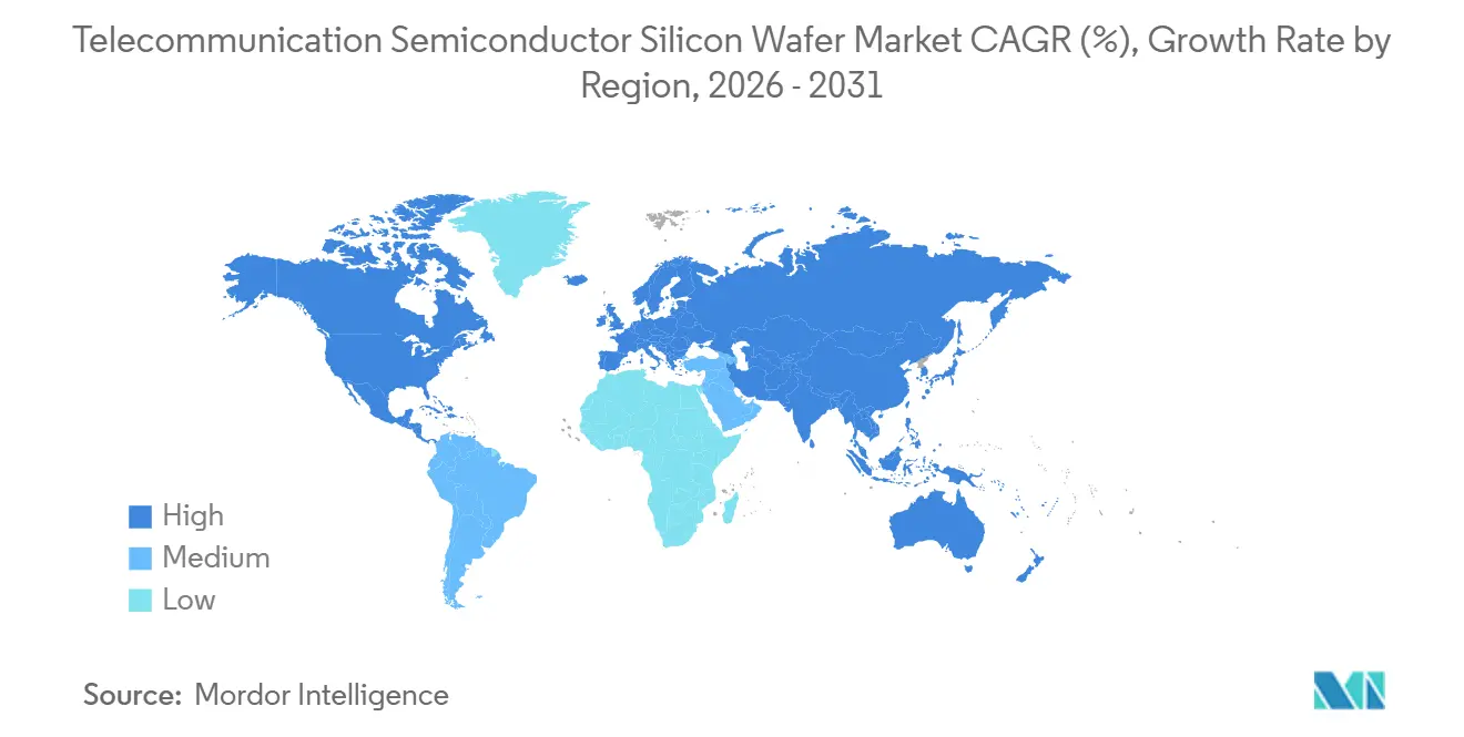
| Fastest Growing Market | Asia Pacific |
| Largest Market | Asia Pacific |
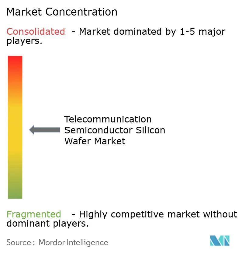
| Market Concentration | Medium |
Major Players *Disclaimer: Major Players sorted in no particular order Image © Mordor Intelligence. Reuse requires attribution under CC BY 4.0. | |
Telecommunication Semiconductor Silicon Wafer Market Analysis by Mordor Intelligence
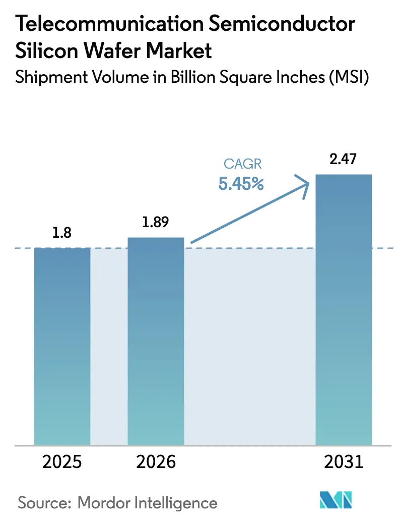
The Telecommunication Semiconductor Silicon Wafer Market size in terms of shipment volume is expected to grow from 1.8 Billion Square Inches (MSI) in 2025 to 1.89 Billion Square Inches (MSI) in 2026 and is forecast to reach 2.47 Billion Square Inches (MSI) by 2031 at 5.45% CAGR over 2026-2031.
An industry pivot toward 5G massive-MIMO base stations, early 6G research platforms, and silicon photonics transceivers is redefining substrate purity, diameter, and defect-density requirements. Government CHIPS-style incentives, particularly in the United States, the European Union, Japan, and South Korea, are encouraging domestic wafer-fab construction, shortening supply chains that were historically concentrated in East Asia. Consolidation among six global suppliers is reinforcing an oligopolistic pricing structure, while new Chinese entrants remain capacity-constrained by export controls on sub-14-nanometer equipment. At the same time, stricter environmental regulations on slurry waste and escalating capital intensity are putting pressure on cost structures, nudging the telecommunication semiconductor silicon wafer market toward higher value specialty substrates.
Key Report Takeaways
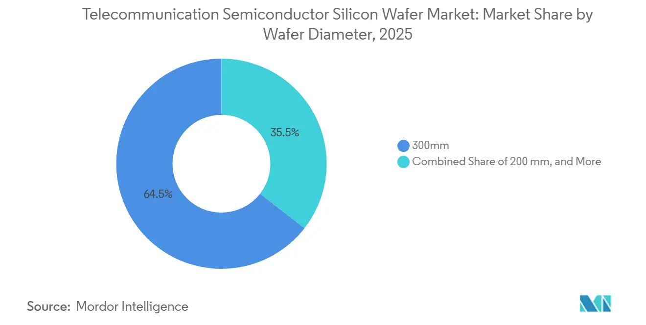
- By wafer diameter, the 300 mm segment led with 64.48% of the telecommunication semiconductor silicon wafer market share in 2025 and is advancing at a 6.01% CAGR through 2031.
- By semiconductor device type, logic devices captured 41.46% of the telecommunication semiconductor silicon wafer market size in 2025 and are expanding at 6.25% CAGR to 2031.
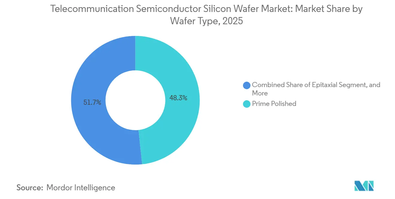
- By wafer type, prime-polished wafers accounted for 48.33% share of the telecommunication semiconductor silicon wafer market size in 2025, whereas silicon-on-insulator substrates are the fastest growing at 6.23% through 2031.
- By geography, Asia-Pacific commanded 80.11% volume in 2025 while recording the fastest regional CAGR at 6.78% through 2031.
Note: Market size and forecast figures in this report are generated using Mordor Intelligence’s proprietary estimation framework, updated with the latest available data and insights as of January 2026.
Global Telecommunication Semiconductor Silicon Wafer Market Trends and Insights
Drivers Impact Analysis*
| Driver | (~) % Impact on CAGR Forecast | Geographic Relevance | Impact Timeline |
|---|---|---|---|
| Surging 5G/6G base-station deployments demanding high-purity 300 mm wafers | +1.8% | Global, concentrated in Asia-Pacific, North America, Europe | Medium term (2-4 years) |
| Government CHIPS-style incentives accelerating telecom-centric wafer fabs | +1.5% | North America, Europe, Japan, South Korea | Long term (≥ 4 years) |
| Rapid adoption of silicon photonics transceivers boosting SOI wafer demand | +1.2% | Global, led by North America and Asia-Pacific data-center hubs | Medium term (2-4 years) |
| Expansion of 300 mm capacity for cloud and edge data-traffic processors | +0.9% | Asia-Pacific core, spill-over to North America and Europe | Long term (≥ 4 years) |
| Ultra-thin wafer demand for co-packaged optics driving new grinding chemistries | +0.6% | North America and Asia-Pacific advanced-packaging clusters | Medium term (2-4 years) |
| Back-side power-delivery ready wafers for AI-powered base-station SoCs | +0.5% | North America, Taiwan, South Korea | Long term (≥ 4 years) |
| Source: Mordor Intelligence | |||
Surging 5G/6G Base-Station Deployments Demanding High-Purity 300 mm Wafers
Massive-MIMO base stations require gallium-nitride power amplifiers and silicon RF front-ends fabricated on 300 mm substrates that must exceed 1,000 ohm-centimeter resistivity to limit substrate losses at frequencies above 3.5 GHz. Global silicon wafer shipments climbed to 12.973 billion square inches in 2025, largely driven by telecom demand.[1]SEMI, “Silicon Shipment Statistics Q4 2025,” SEMI.ORG Imec validated GaN-on-silicon RF transistors operating in the 7-24 GHz band, designated for 6G, extending wafer consumption beyond current 5G needs.[2] Imec, “GaN-on-Silicon RF Transistors 2025,” IMEC-INT.COM China Mobile and China Telecom deployed a combined 1.2 million 5G sites by 2025, each using roughly 200-300 square inches of silicon. Only two suppliers consistently meet the parts-per-trillion metallic contamination threshold required for millimeter-wave applications.
Government CHIPS-Style Incentives Accelerating Telecom-Centric Wafer Fabs
The US CHIPS and Science Act reserved USD 36.4 billion across 40 projects by 2025, with GlobalWafers obtaining USD 400 million for twin 300 mm plants in Texas and Missouri. Texas Instruments secured USD 1.6 billion in funding, earmarked for four 300 mm fabs that feed base-station backhaul and power-supply ICs. Europe committed EUR 43 billion (USD 46 billion) under its Chips Act, underwriting Infineon and STMicroelectronics' capacity for RF and power wafers. Japan’s JPY 920 billion (USD 6.2 billion) subsidy package is ensuring 300 mm substrate availability for 5G despite geopolitical frictions. These grants lower effective capital costs 25-35%, compressing payback times to under 10 years.
Rapid Adoption of Silicon Photonics Transceivers Boosting SOI Wafer Demand
Silicon photonics integrates lasers, modulators, and photodetectors on silicon-on-insulator wafers, enabling 800G and 1.6T transceivers now favored in metro and long-haul networks. Tower Semiconductor and NVIDIA are migrating photonics production to 300 mm, projecting 40% cost savings per transceiver. OpenLight has volume orders for 1.6T photonic integrated circuits that blend indium phosphide with silicon. SOITEC’s photonics-grade SOI wafers rose to 18% of revenue in fiscal 2024, evidencing telecom’s appetite for co-packaged optics.[3]Soitec, “Annual Report 2024,” SOITEC.COM The IEEE roadmap foresees silicon photonics capturing 30% of optical transceiver shipments by 2028.
Expansion of 300 mm Capacity for Cloud and Edge Data-Traffic Processors
Edge-computing nodes that stream video analytics and industrial IoT telemetry are driving demand for 7-16 nm ASICs built on 300 mm wafers. GlobalWafers’ Sherman plant began shipping 1.2 million 300 mm wafers yearly in May 2025, meeting sub-10-nanometer defect specifications. Bosch’s Dresden fab uses AI-based process control to reduce wafer-to-wafer variation to below 1%, boosting yields for mixed-signal base-station chips. Migration to chiplet designs increases wafer consumption by 15-20% per device, favoring 300 mm wafers due to lower per-die costs.
Restraints Impact Analysis*
| Restraint | (~) % Impact on CAGR Forecast | Geographic Relevance | Impact Timeline |
|---|---|---|---|
| Capital intensity and long payback periods for 300 mm wafer lines | -1.2% | Global, especially in regions without subsidies | Long term (≥ 4 years) |
| Defect-density challenges with high-resistivity RF-grade wafers | -0.8% | Global, higher impact in Asia-Pacific and North America RF hubs | Medium term (2-4 years) |
| Export-control restrictions on advanced wafer-equipment shipments | -0.6% | China, secondary effects in Southeast Asia and Russia | Medium term (2-4 years) |
| Stricter slurry-waste regulations impacting photonics-grade CMP costs | -0.4% | North America and Europe, emerging compliance in Asia-Pacific | Short term (≤ 2 years) |
| Source: Mordor Intelligence | |||
Capital Intensity and Long Payback Periods for 300 mm Wafer Lines
A single greenfield 300 mm plant costs USD 3-5 billion, with equipment absorbing up to 70% of outlay. Siltronic’s Singapore expansion illustrates the challenge, spending EUR 2 billion (USD 2.14 billion) for 1 million wafers per year. Even entrenched firms like SUMCO and SK Siltron formed a joint venture to share a USD 3.6 billion build-out. Where subsidies cover less than 15% of costs, investors face 10-15 year payback horizons,[4]Financial Times, “Semiconductor Capital Intensity Analysis,” FT.COM deterring new entrants and reinforcing the oligopoly.
Defect-Density Challenges with High-Resistivity RF-Grade Wafers
High-resistivity wafers, crucial for millimeter-wave RF applications, are grappling with defect counts that are 20-30% higher than those found in standard substrates. Soitec has introduced a trap-rich solution that effectively reduces these defects to below 0.1 particles per cm². However, this innovation comes at a premium, increasing costs by 15-20%. Additionally, with yield losses ranging between 8-12%, some designers are reconsidering their choices and reverting to gallium-arsenide, even though it comes with a steeper material cost. Furthermore, the advanced inspection equipment from KLA is adding an extra USD 10-15 million to the cost of each production line.
*Our forecasts treat driver/restraint impacts as directional, not additive. The impact forecasts reflect baseline growth, mix effects, and variable interactions.
Segment Analysis
By Wafer Diameter: 300 mm Scale Economics Sustain Leadership
The 300 mm segment controlled 64.48% of volume in 2025, reflecting per-die savings of 30-40% and automation advantages. GlobalWafers’ Sherman site shipped its first 1.2 million wafers in 2025, underscoring domestic momentum. Texas Instruments joined with four 40,000-wspm modules to feed analog and embedded telecom ICs. Equipment shortages keep 200 mm capacity tight, nudging redesigns onto 300 mm lines. Sub-150-mm wafers remain a niche for GaN power RF amplifiers and MEMS antenna tuners, yet continue to cede market share. Regulatory bodies have little sway over diameter choice, though export controls on 300 mm tools to China slow adoption there.
As chiplet architectures rise, each radio front-end now requires multiple dies across power, RF, and digital domains, inflating demand for larger substrates. The telecommunication semiconductor silicon wafer market sees suppliers bundling prime-polished and epitaxial variants to lock in volume. Industry consortia like SEMI standardize notch positions and thickness tolerances, allowing fabs to quickly qualify multiple sources, which tempers supplier power marginally but keeps barriers high for new entrants.


By Semiconductor Device Type: Logic Integration Anchors Consumption
Logic devices accounted for 41.46% of wafers in 2025, driven by base-station SoCs that consolidate RF transceivers, digital baseband, and power management on a single die. High-bandwidth memory now teams with AI accelerators in radio units, nudging DRAM demand but still trailing logic. Analog devices, including RF switches and LNAs, rely on high-resistivity and SOI wafers that cost 20-30% more than prime-polished wafers, yet customers absorb the premium to meet linearity and loss targets. Discrete GaN power transistors are available on smaller wafers yet remain critical for 48 V power rails.
Optoelectronics joins the fold as silicon photonics transceivers move on board, creating hybrid demand streams that suppliers must balance. Foundries report double-digit order growth for logic epitaxial wafers aligned with chiplet strategies, and telecom OEMs prefer single-die integration to cut board area, which explains the sustained edge of logic in the telecommunication semiconductor silicon wafer market.
By Wafer Type: SOI Outpaces but Prime-Polished Holds Volume
Prime-polished wafers held a 48.33% share in 2025, underpinned by cost leadership in mainstream logic. Yet SOI substrates are expanding 6.23% annually, buoyed by buried-oxide layers that reduce capacitance 30-50% in RF switches and by low-loss photonics waveguides. Epitaxial wafers gain as 7-10 nm logic migrates into virtualized radio access architectures. Specialty silicon, including high-resistivity variants, commands a premium but remains volume-restricted due to limited supply.
Soitec is doubling 300 mm SOI capacity at Bernin to furnish co-packaged optics, while Okmetic positions sensor-grade silicon for antenna beam-tilt MEMS. Pricing trends show prime-polished growth moderating as telecom shifts to higher-value substrates, a dynamic that cements SOI’s role despite its premium in the telecommunication semiconductor silicon wafer market.
Geography Analysis
Asia-Pacific supplied 80.11% of wafers in 2025 and posts a 6.78% CAGR to 2031. China’s 1.2 million 5G base stations create captive demand that domestic suppliers rush to serve, though tool embargoes keep yields below Japanese levels. Japan’s Shin-Etsu and SUMCO together furnish about 55% of global 300 mm capacity, leveraging unmatched Czochralski expertise. South Korea’s SUMCO-SK Siltron venture adds 1 million wafers annually by 2027, with telecom and automotive as anchor segments. Taiwan remains a voracious consumer through foundry leader TSMC, whose Kumamoto site secures JPY 920 billion (USD 6.2 billion) state backing.
North America gains momentum from USD 36.4 billion CHIPS Act funding. GlobalWafers and Texas Instruments collectively deliver 2 million 300 mm wafers by 2027, trimming reliance on Asian imports. Europe’s EUR 43 billion (USD 46 billion) Chips Act bankrolls Infineon and STMicroelectronics expansions, yet its share lingers below 10% because of elevated energy and labor costs. South America and the Middle East and Africa remain small, importing wafers for limited 5G rollouts.
Export controls by the United States, Japan, and the Netherlands on sub-14 nm equipment fragment the Asia-Pacific chain, forcing Chinese fabs onto 28 nm and enlarging wafer area per function by up to 60%. China’s retaliatory curbs on gallium and germanium raise compound-semiconductor costs, shifting demand to Japanese and Korean suppliers that enjoy diversified feedstock. Supply-chain diversification efforts will show material impact only after 2030 due to 10-15 year payback cycles for new fabs.

Competitive Landscape
Six incumbents, Shin-Etsu Chemical, SUMCO, GlobalWafers, Siltronic, SK Siltron, and Soitec, control about 85% of 300 mm capacity, granting moderate pricing power yet exposing buyers to concentration risk. Shin-Etsu’s in-house polysilicon hedges raw-material volatility, while GlobalWafers pursues rapid U.S. scaling to capture reshoring incentives. Siltronic banks on AI-enhanced process control to win defect-sensitive logic accounts.
Chinese entrants National Silicon Industry Group and Zhonghuan Semiconductor expand under export-equipment limits, tapping 200 mm lines and pushing yields through domestic tool development. Smaller niche firms such as Okmetic and Ferrotec focus on ultra-thin and specialty wafers where incumbent scale economies matter less.
Strategic themes include subsidy-backed capacity adds, joint ventures for capital sharing, and customer road-mapping partnerships. SUMCO-SK Siltron’s USD 3.6 billion collaboration typifies risk pooling, while Tower Semiconductor’s photonics alliance with NVIDIA embeds the supplier deep into future optical roadmaps. Patent filings reveal incumbents investing in ultra-thin handling, buried defect analytics, and epitaxial uniformity, sustaining gross margins above 30% even as telecommunication semiconductor silicon wafer market volumes grow.
Telecommunication Semiconductor Silicon Wafer Industry Leaders
Shin-Etsu Chemical Co., Ltd.
SUMCO Corporation
GlobalWafers Co., Ltd.
Siltronic AG
SK Siltron Co., Ltd
- *Disclaimer: Major Players sorted in no particular order

Recent Industry Developments
- January 2026: Tower Semiconductor unveiled its 300 mm silicon photonics platform in partnership with NVIDIA, promising 40% cost reductions versus 200 mm processing.
- December 2025: Texas Instruments began production at its Sherman, Texas mega-site, the first of four 300 mm fabs funded with USD 1.6 billion in CHIPS Act grants.
- May 2025: GlobalWafers opened its USD 3.5 billion 300 mm wafer plant in Sherman, Texas, with 1.2 million wafers per year initial capacity.
- April 2025: Soitec posted EUR 1.09 billion (USD 1.16 billion) fiscal 2024 revenue and announced a Bernin expansion to boost 300 mm SOI output.


Global Telecommunication Semiconductor Silicon Wafer Market Report Scope
The Telecommunication Semiconductor Silicon Wafer Market Report is Segmented by Wafer Diameter (Up to 150mm, 200mm, 300mm), Semiconductor Device Type (Logic, Memory, Analog, Discrete, Other Types), Wafer Type (Prime Polished, Epitaxial, Silicon-on-Insulator, Specialty Silicon), and Geography (North America, Europe, Asia-Pacific, South America, Middle East and Africa). Market Forecasts are Provided in Terms of Volume (Million Square Inches).
| Up to 150 mm |
| 200 mm |
| 300 mm |
| Logic |
| Memory |
| Analog |
| Discrete |
| Other Semiconductor Device Types (Optoelectronics, Sensors, Micro) |
| Prime Polished |
| Epitaxial |
| Silicon-on-Insulator (SOI) |
| Specialty Silicon (High-Resistivity, Power, Sensor-Grade) |
| North America | United States |
| Canada | |
| Mexico | |
| Europe | Germany |
| United Kingdom | |
| France | |
| Rest of Europe | |
| Asia-Pacific | China |
| Japan | |
| India | |
| South Korea | |
| Taiwan | |
| Rest of Asia-Pacific | |
| South America | |
| Middle East | |
| Africa |
| By Wafer Diameter | Up to 150 mm | |
| 200 mm | ||
| 300 mm | ||
| By Semiconductor Device Type | Logic | |
| Memory | ||
| Analog | ||
| Discrete | ||
| Other Semiconductor Device Types (Optoelectronics, Sensors, Micro) | ||
| By Wafer Type | Prime Polished | |
| Epitaxial | ||
| Silicon-on-Insulator (SOI) | ||
| Specialty Silicon (High-Resistivity, Power, Sensor-Grade) | ||
| By Geography | North America | United States |
| Canada | ||
| Mexico | ||
| Europe | Germany | |
| United Kingdom | ||
| France | ||
| Rest of Europe | ||
| Asia-Pacific | China | |
| Japan | ||
| India | ||
| South Korea | ||
| Taiwan | ||
| Rest of Asia-Pacific | ||
| South America | ||
| Middle East | ||
| Africa | ||


Key Questions Answered in the Report
How large will global telecom-grade silicon wafer consumption be by 2031?
Volume is forecast to reach 2,468.23 million square inches by 2031, representing a 5.45% CAGR from 2026.
Which wafer diameter dominates telecom equipment fabrication?
300 mm wafers led with 64.48% share in 2025 because of 30-40% per-die cost savings over 200 mm.
Why is silicon-on-insulator gaining in radio hardware?
SOI’s buried oxide reduces RF capacitance and optical loss, yielding the fastest growth at 6.23% through 2031.
What regions benefit most from CHIPS-style subsidies?
North America, Europe, Japan, and South Korea receive multibillion-dollar incentives that cut capital costs up to 35%.
Who are the top suppliers of telecom-grade silicon wafers?
Shin-Etsu Chemical, SUMCO, GlobalWafers, Siltronic, SK Siltron, and Soitec collectively hold about 85% of 300 mm capacity.
Page last updated on:


