SOI Silicon Wafer Market Size and Share
Market Overview
| Study Period | 2020 - 2031 |
|---|---|
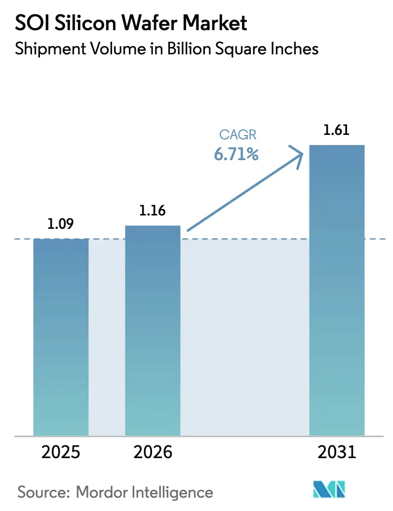
| Market Volume (2026) | 1.16 Billion Square Inches |
| Market Volume (2031) | 1.61 Billion Square Inches |
| Growth Rate (2026 - 2031) | 6.71% CAGR |
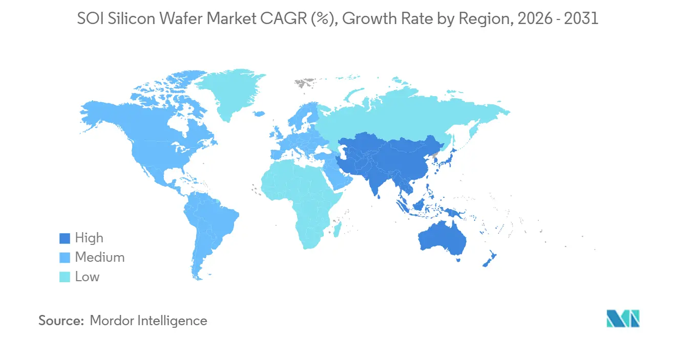
| Fastest Growing Market | Asia Pacific |
| Largest Market | Asia Pacific |
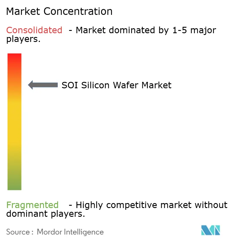
| Market Concentration | High |
Major Players *Disclaimer: Major Players sorted in no particular order Image © Mordor Intelligence. Reuse requires attribution under CC BY 4.0. | |
SOI Silicon Wafer Market Analysis by Mordor Intelligence
The SOI silicon wafer market size was 1.09 billion square inches in 2025 and is estimated to grow from 1.16 billion square inches in 2026 to reach 1.61 billion square inches by 2031, at a CAGR of 6.71% during the forecast period (2026-2031). Momentum stems from 5G radio-frequency front-end modules, automotive power-management ICs, and silicon-photonics interconnects that demand the dielectric isolation and back-bias flexibility SOI provides. Capacity constraints on 300 mm substrates, a persistent 2-to-3-times cost premium over bulk silicon, and the intellectual-property moat around Soitec’s Smart Cut process temper growth but do not derail adoption, because foundry roadmaps now favor fully depleted SOI nodes over bulk CMOS at 28 nm and below. Asia-Pacific dominates shipments, yet policy-driven capacity additions in the United States and Europe are reshaping geographic risk. Device makers therefore juggle performance gains against wafer availability and unit economics as they plan long-term supply strategies for the SOI silicon wafer market.
Key Report Takeaways
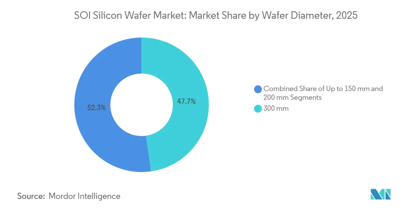
- By wafer diameter, the 300 mm segment accounted for 47.74% of 2025 volume and is forecast to post a 7.17% CAGR through 2031, outpacing 200 mm and smaller formats.
- By semiconductor device type, logic devices led with 36.61% of the SOI silicon wafer market share in 2025, while discrete and power semiconductors are projected to expand at a 7.29% CAGR to 2031.
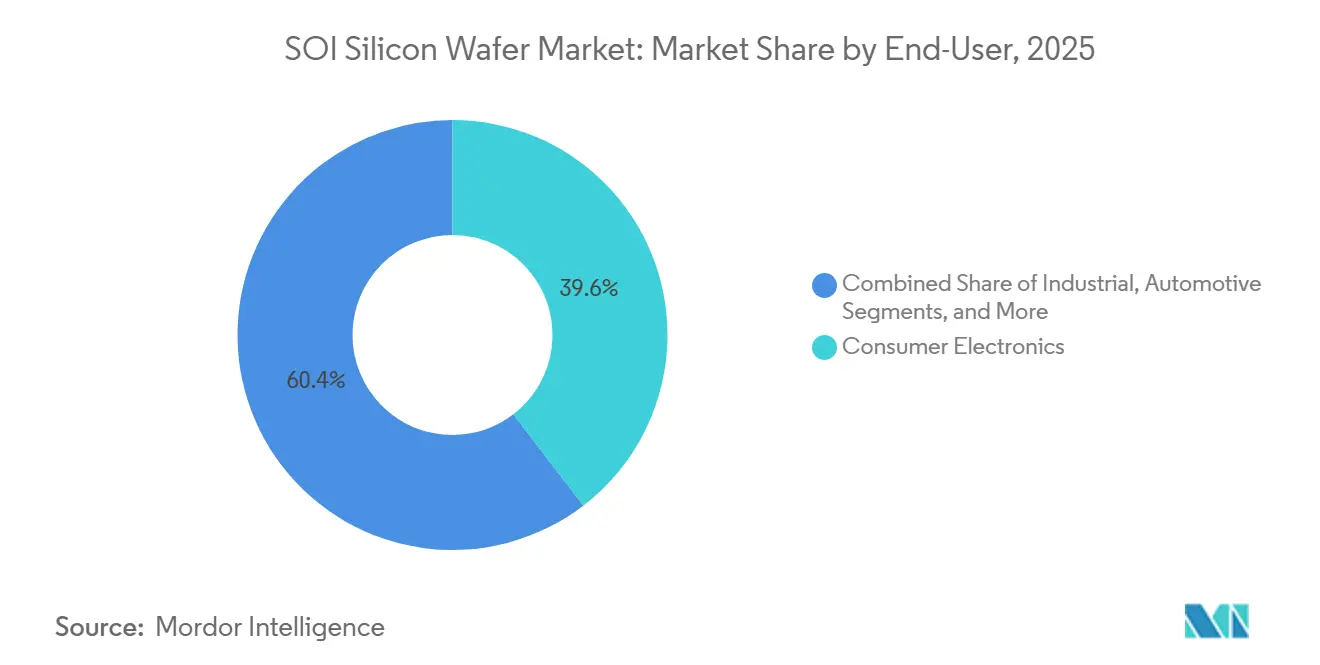
- By end-user, consumer electronics retained 39.59% share in 2025, whereas automotive applications are advancing at a market-leading 7.36% CAGR during 2026-2031.
- By geography, Asia-Pacific commanded 83.22% of 2025 volume and is expected to grow at a 7.22% CAGR, maintaining clear volume leadership through 2031.
Note: Market size and forecast figures in this report are generated using Mordor Intelligence’s proprietary estimation framework, updated with the latest available data and insights as of January 2026.
Global SOI Silicon Wafer Market Trends and Insights
Drivers Impact Analysis*
| Driver | (~) % Impact on CAGR Forecast | Geographic Relevance | Impact Timeline |
|---|---|---|---|
| Rapid Adoption of FD-SOI for 5G RF Front-end Modules | +1.2% | Global, with concentration in Asia-Pacific and North America | Short term (≤ 2 years) |
| Increasing Integration of SOI in Automotive ADAS and Power Management ICs | +1.5% | Global, led by Europe and North America, expanding in Asia-Pacific | Medium term (2-4 years) |
| Government Incentives for Domestic 300 mm SOI Fabs in Asia and Europe | +1.0% | United States, European Union, Japan, South Korea | Medium term (2-4 years) |
| Demand Surge from Silicon Photonics in Hyperscale Data Centers | +1.3% | North America, Europe, Asia-Pacific hyperscale hubs | Short term (≤ 2 years) |
| Emerging Neuromorphic and Quantum Computing Control Chips on SOI Substrates | +0.6% | North America, Europe, select Asia-Pacific research clusters | Long term (≥ 4 years) |
| Transition Toward Mixed-Signal IoT Devices Requiring Ultra-Low-Leakage SOI Nodes | +0.8% | Global, with early adoption in Asia-Pacific and North America | Medium term (2-4 years) |
| Source: Mordor Intelligence | |||
Rapid Adoption of FD-SOI for 5G RF Front-End Modules
Radio-frequency front-end modules for 5G and early 6G smartphones increasingly rely on RF-SOI and FD-SOI substrates to satisfy linearity and insertion-loss targets at millimeter-wave frequencies, where bulk CMOS struggles. GlobalFoundries’ 9SW platform integrates switches and low-noise amplifiers on 300 mm RF-SOI, enabling handset makers to shrink board area by 30% while meeting stringent power budgets.[1]GlobalFoundries Inc., “9SW RF-SOI Launch,” GLOBALFOUNDRIES.COM Tower Semiconductor extended similar technology to Wi-Fi 7, partnering with Broadcom to achieve sub-0.4 dB insertion loss at 6 GHz. High-volume validation arrived when Apple’s iPhone 17 used Qualcomm’s QTM565 antenna module fabricated on 22FDX FD-SOI in early 2026. VeriSilicon has already shipped more than 100 million FD-SOI connectivity chips, underscoring a mainstream shift that widens the addressable SOI silicon wafer market.[2]VeriSilicon Microelectronics, “100 Million FD-SOI Units Shipped,” VERISILICON.COM As handset OEMs pursue 6G integration, substrate suppliers benefit from richer die-area requirements and premium wafer pricing.
Increasing Integration of SOI in Automotive ADAS and Power-Management ICs
Vehicle makers have migrated battery-management ICs and imaging-radar transceivers to SOI to meet ISO 26262 functional-safety standards and to avoid latch-up in 48-volt electrical systems. Soitec’s Power-SOI family supports 200-volt operation, allowing battery-monitor ICs to supervise 30-cell strings without costly isolation stages, cutting bill-of-materials cost by 15%. Automotive radar revenue is on track to reach USD 22 billion by 2030, and 22 nm FD-SOI processes deliver transit frequencies above 350 GHz, aligning with 4D radar requirements.[3]IEEE, “Automotive Radar Forecast 2021-2030,” IEEE.ORG STMicroelectronics and NXP have qualified 300 mm Power-SOI lines, signaling volume readiness. As electric-vehicle production climbs, discrete power and mixed-signal processors built on SOI are becoming default choices, lifting the long-term growth outlook for the SOI silicon wafer market.
Government Incentives for Domestic 300 mm SOI Fabs in Asia and Europe
Sovereign semiconductor programs now explicitly fund specialty-wafer capacity to reduce import dependence. The United States CHIPS and Science Act awarded GlobalWafers USD 400 million to build a 300 mm SOI line in Missouri and to enlarge facilities in Texas. The European Union Chips Act co-financed GlobalWafers’ FAB300 in Novara, Italy, at EUR 450 million (USD 495 million). Japan’s subsidies to Shin-Etsu Chemical and SUMCO target incremental 300 mm SOI output, while South Korea’s package supports SK Siltron’s upgrades. These incentives shave 30-40% off capital costs, accelerate time-to-volume, and geographically diversify the SOI silicon wafer market, although meaningful capacity relief will not arrive until late 2027.
Demand Surge from Silicon Photonics in Hyperscale Data Centers
Cloud providers are shifting to silicon photonics transceivers at 800 Gbps and 1.6 Tbps, technologies that require photonics-grade SOI with carefully tuned buried oxide layers. The silicon photonics segment is set to triple between 2026 and 2031, fueled by co-packaged optics that place modulators and lasers alongside switch ASICs. Soitec’s Photonics-SOI substrates reduce optical loss and improve thermal stability, enabling energy savings of up to 50% in switch fabrics. Intel, Cisco, and Marvell have each announced roadmaps that standardize on Photonics-SOI interposers, locking in multi-year volumes. Because photonics relies on buried oxide for waveguide confinement, bulk silicon is not a viable substitute, creating a structural growth pillar for the SOI silicon wafer market.
Restraints Impact Analysis*
| Restraint | (~) % Impact on CAGR Forecast | Geographic Relevance | Impact Timeline |
|---|---|---|---|
| Limited Global Capacity for 300mm SOI Wafer Production | -0.8% | Global, with acute shortages in North America and Europe | Short term (≤ 2 years) |
| Higher Cost Premium Over Bulk Silicon Substrates | -0.7% | Global, with price sensitivity highest in consumer electronics | Medium term (2-4 years) |
| Wafer Edge-Void Defects Causing Yield Losses in Advanced FD-SOI Nodes | -0.4% | Foundries ramping 22nm and 12nm FD-SOI in Europe and Asia-Pacific | Short term (≤ 2 years) |
| Intellectual-Property Concentration Around Smart Cut and Eltran Processes | -0.3% | Global, constraining new entrants in all regions | Long term (≥ 4 years) |
| Source: Mordor Intelligence | |||
Limited Global Capacity for 300 mm SOI Wafer Production
Worldwide, 300 mm SOI output remains below 3 million wafers per year, less than 2% of the total 300 mm bulk-silicon supply. Soitec’s Bernin and Singapore plants deliver roughly 2 million wafers, while Shin-Etsu and SUMCO contribute only 0.5 million. Okmetic’s 2026 expansion addressed 200 mm demand rather than 300 mm, leaving a capacity gap until GlobalWafers’ U.S. and Italian plants reach volume in late 2027. Scarcity forces foundries into multi-quarter commitments, raises substrate prices by single-digit percentages each year, and threatens to cap near-term growth for the SOI silicon wafer market until new lines come online.
Higher Cost Premium Over Bulk Silicon Substrates
A 300 mm SOI blank costs USD 800-1,500 versus USD 100-150 for a bulk-silicon wafer, reflecting expensive implant, bond, and split steps. The premium narrows viable markets to RF, automotive, and photonics devices where performance gains offset price. Entry-level smartphones and IoT sensors often remain on bulk CMOS, blunting penetration. Process innovations such as wafer reclaim promise relief, but until they scale, wafer cost will constrain expansion in price-elastic segments and weigh on the long-term trajectory of the SOI silicon wafer market.
*Our forecasts treat driver/restraint impacts as directional, not additive. The impact forecasts reflect baseline growth, mix effects, and variable interactions.
Segment Analysis
By Wafer Diameter – 300 mm: Migrating to Large-Wafer Economics
The 300 mm segment accounted for 47.74% of 2025 volume and is projected to expand at a 7.17% CAGR to 2031, making it the primary volume driver for the SOI silicon wafer market size over the forecast horizon. Foundries including GlobalFoundries, STMicroelectronics, and Tower Semiconductor have standardized RF-SOI and FD-SOI processes on 300 mm equipment to capture die-cost savings and to reuse mature tool sets already optimized for low-defect density. As new 5G, Wi-Fi 7, and automotive radar designs transit from 200 mm to 300 mm flows, substrate demand accelerates, further lifting the SOI silicon wafer market.
Advances in automotive Power-SOI, however, still rely on 200 mm lines because those fabs are fully depreciated and already qualified for long model-year lifecycles. Until global demand justifies the USD 100 million investment per Smart Cut line at 300 mm, suppliers will keep a hybrid footprint. Sub-150 mm formats retain niche relevance in radiation-hardened aerospace electronics, where qualification cycles run a decade or longer. Consequently, the wafer-diameter mix will remain bifurcated, but the revenue center of the SOI silicon wafer market will continue to pivot toward 300 mm substrates through 2031.


By Semiconductor Device Type – Logic Leads, Discrete and Power Accelerate
Logic devices held 36.61% of the SOI silicon wafer market share in 2025, reflecting dominance in RF transceivers, baseband processors, and connectivity chips built on RF-SOI and FD-SOI. The discrete and power segment, although smaller, is forecast to grow at 7.29% CAGR, the fastest among device categories, as 48-volt electrical systems in vehicles and isolated gate drivers in renewable inverters migrate to Power-SOI. This shift directly lifts the SOI silicon wafer market size attributed to power applications.
Analog ICs, such as data converters and sensor interfaces, enjoy lower parasitic capacitance on SOI, supporting their steady expansion. Memory on SOI remains experimental outside embedded caches inside neuromorphic accelerators. By 2031, power devices are expected to overtake analog as the second-largest volume category, altering the long-standing logic-centric profile of the SOI silicon wafer market.
By End-User – Consumer Electronics Dominates, Automotive Surges
Consumer electronics consumed 39.59% of SOI wafers in 2025, driven by front-end modules in smartphones, tablets, and wearables. Although handset volume growth is plateauing, device complexity is rising, preserving substrate demand. Automotive applications, meanwhile, are on course for a 7.36% CAGR as advanced driver-assistance systems transition to 4D radar and electric-vehicle inverters adopt integrated high-side switch drivers on Power-SOI, collectively lifting the SOI silicon wafer market size allocated to vehicles.
Industrial and telecommunications infrastructure users post mid-single-digit growth based on factory automation and 5G small-cell deployment cycles. Aerospace, defense, and medical markets remain niche but strategically important, because they validate SOI in extreme environments. The evolving end-user mix reduces exposure to handset saturation and broadens the revenue base for the SOI silicon wafer market.
Geography Analysis
Asia-Pacific held 83.22% of 2025 shipments and is set to maintain volume leadership with a 7.22% CAGR through 2031. Taiwan’s foundries anchor regional demand, while Japan’s Shin-Etsu and SUMCO provide local substrate supply. China is ramping domestic 200 mm SOI at Shanghai Simgui and researching 300 mm capacity to reduce reliance on imports, further expanding the regional SOI silicon wafer market.
North America is poised for accelerated growth once GlobalWafers’ Missouri and Texas plants come online in 2027, offering a domestic supply to automotive, defense, and telecom customers that prize secure sourcing. Europe follows a parallel path; STMicroelectronics’ 300 mm FD-SOI fab in Crolles and GlobalWafers’ Novara plant, supported by EU Chips Act funding, aim to mitigate supply-chain risk and meet the needs of regional OEMs that require origin compliance. Together, these developments diversify the global SOI silicon wafer market away from its current Asia-heavy base.
South America and the Middle East, and Africa account for marginal volumes, constrained by limited foundry infrastructure. Nonetheless, Israel’s Tower Semiconductor does supply global RF-SOI modules from its local fabs, maintaining a modest Middle Eastern footprint. Regional diversification trends will continue as governments tie subsidies to domestic capacity, incrementally lowering geopolitical risk across the SOI silicon wafer market.

Competitive Landscape
The SOI silicon wafer market is highly concentrated. Soitec controls roughly half of the global supply through its patented Smart Cut process and long-term contracts with GlobalFoundries, STMicroelectronics, and Tower Semiconductor. Shin-Etsu Chemical, SUMCO, and GlobalWafers share the remaining 30%, leveraging licensed or proprietary bonding flows on repurposed bulk-silicon lines. Foundry alignment is critical because process qualifications effectively lock in substrate vendors for multi-year cycles.
Strategic moves over the past 18 months illustrate this dynamic. GlobalFoundries launched its 9SW RF-SOI platform on Soitec wafers to capture mmWave front-end demand, while Tower Semiconductor and Broadcom jointly rolled out Wi-Fi 7 modules on Tower’s 300 mm RF-SOI line, again using Soitec substrates. To reduce vulnerability to a single supplier, GlobalWafers is adding European and U.S. capacity, and Samsung is studying in-house SOI production to secure captive automotive and RF needs.
Meanwhile, Chinese entrants such as Shanghai Simgui receive state backing but remain technologically one node behind incumbents. Intellectual-property barriers limit disruptive entry, yet policy-driven capex plus niche photonics and power opportunities could shift share at the margin, prompting incumbents to quicken yield and cost improvements to defend their positions in the SOI silicon wafer market.
SOI Silicon Wafer Industry Leaders
Soitec SA
Shin-Etsu Chemical Co., Ltd.
SUMCO Corporation
GlobalWafers Co., Ltd.
National Silicon Industry Group
- *Disclaimer: Major Players sorted in no particular order

Recent Industry Developments
- February 2026: Okmetic began volume output of 150 mm and 200 mm SOI wafers at its expanded Vantaa, Finland fab, adding Power-SOI capacity for automotive battery-management ICs and industrial motor drives.
- January 2026: Wolfspeed unveiled 300 mm silicon-carbide wafers, promising 30% die-cost reduction and intensifying competition versus Power-SOI in high-voltage mobility converters.
- October 2025: GlobalWafers opened its FAB300 in Novara, Italy at EUR 450 million (USD 495 million), focusing on 300 mm SOI substrates for automotive and industrial customers.
- September 2025: Tower Semiconductor partnered with Broadcom to deliver RF-SOI Wi-Fi 7 front-end modules with sub-0.4 dB insertion loss at 6 GHz.


Global SOI Silicon Wafer Market Report Scope
The SOI Silicon Wafer Market Report is Segmented by Wafer Diameter (Up to 150mm, 200mm, and 300mm), Semiconductor Device Type (Logic, Memory, Analog, Discrete, and Other Device Type), End-user (Consumer Electronics, Industrial, Telecommunications, Automotive, and Other End-users), and Geography (North America, Europe, Asia-Pacific, South America, Middle East and Africa). The Market Forecasts are Provided in Terms of Volume (Square Inches).
| Up to 150 mm |
| 200 mm |
| 300 mm |
| Logic |
| Memory |
| Analog |
| Discrete |
| Other Semiconductor Device Types |
| Consumer Electronics | Mobile and Smartphones |
| PCs and Servers | |
| Industrial | |
| Telecommunications | |
| Automotive | |
| Other End-user Applications |
| North America | United States |
| Canada | |
| Mexico | |
| Europe | Germany |
| United Kingdom | |
| France | |
| Rest of Europe | |
| Asia-Pacific | China |
| Japan | |
| India | |
| South Korea | |
| Taiwan | |
| Rest of Asia-Pacific | |
| South America | |
| Middle East and Africa |
| By Wafer Diameter | Up to 150 mm | |
| 200 mm | ||
| 300 mm | ||
| By Semiconductor Device Type | Logic | |
| Memory | ||
| Analog | ||
| Discrete | ||
| Other Semiconductor Device Types | ||
| By End-user | Consumer Electronics | Mobile and Smartphones |
| PCs and Servers | ||
| Industrial | ||
| Telecommunications | ||
| Automotive | ||
| Other End-user Applications | ||
| By Geography | North America | United States |
| Canada | ||
| Mexico | ||
| Europe | Germany | |
| United Kingdom | ||
| France | ||
| Rest of Europe | ||
| Asia-Pacific | China | |
| Japan | ||
| India | ||
| South Korea | ||
| Taiwan | ||
| Rest of Asia-Pacific | ||
| South America | ||
| Middle East and Africa | ||


Key Questions Answered in the Report
How large is the SOI silicon wafer market in 2026?
The market stands at 1.16 billion square inches in 2026.
What is the forecast CAGR for SOI substrates through 2031?
The SOI silicon wafer market is projected to grow at a 6.71% CAGR from 2026 to 2031.
Which wafer diameter is growing fastest?
The 300 mm segment is advancing at a 7.17% CAGR, driven by RF-SOI and FD-SOI migrations.
Why are automotive applications adopting SOI rapidly?
Automotive radar and 48-volt power architectures benefit from SOI’s latch-up immunity and high-voltage isolation, supporting a 7.36% CAGR for vehicle demand.
Page last updated on:


