Silicon Wafer for Memory Devices Market Size and Share
Market Overview
| Study Period | 2020 - 2031 |
|---|---|
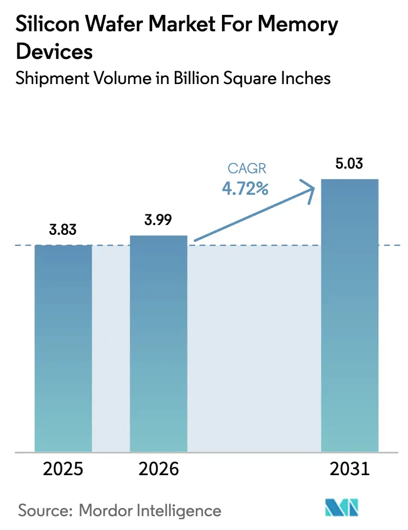
| Market Volume (2026) | 3.99 Billion Square Inches |
| Market Volume (2031) | 5.03 Billion Square Inches |
| Growth Rate (2026 - 2031) | 4.72% CAGR |
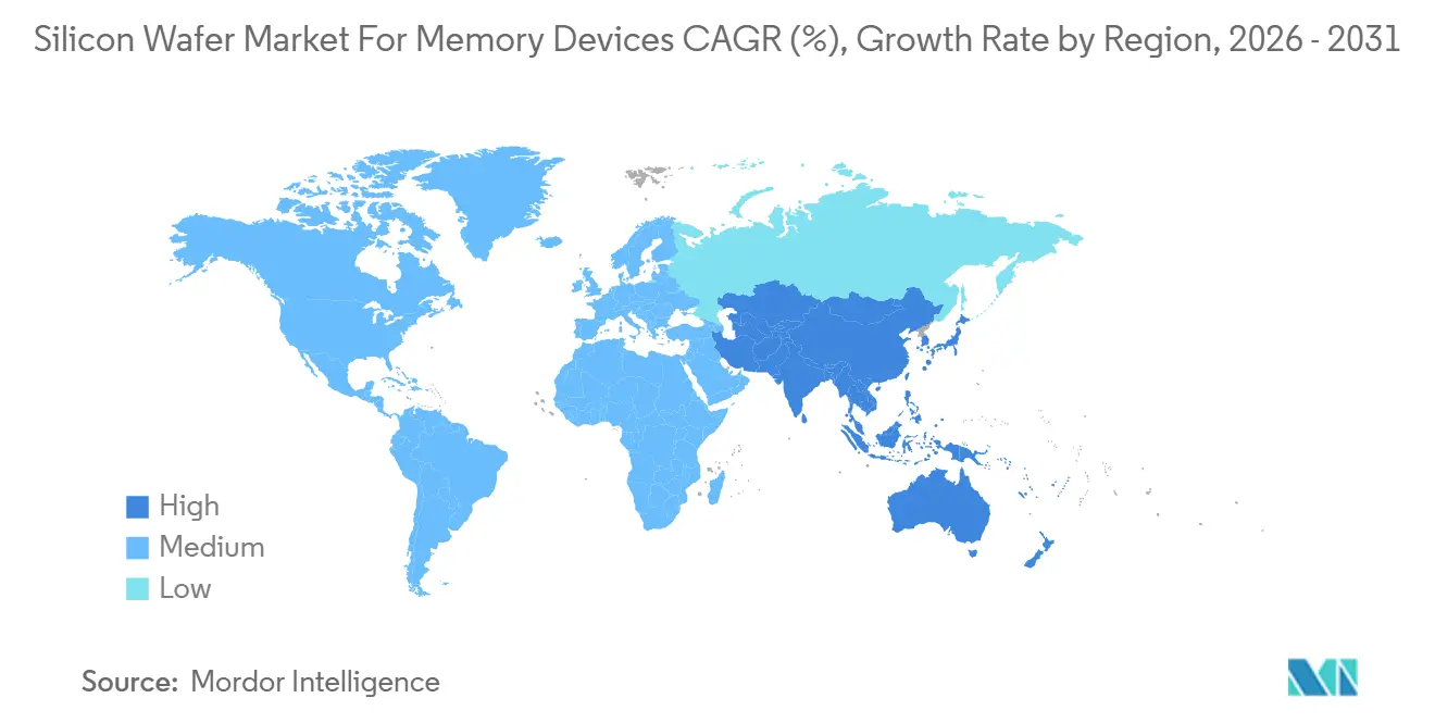
| Fastest Growing Market | Asia Pacific |
| Largest Market | Asia Pacific |
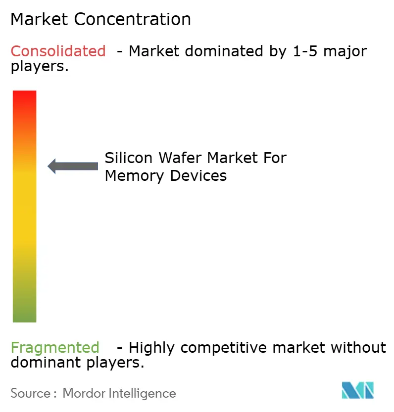
| Market Concentration | Medium |
Major Players *Disclaimer: Major Players sorted in no particular order Image © Mordor Intelligence. Reuse requires attribution under CC BY 4.0. | |
Silicon Wafer for Memory Devices Market Analysis by Mordor Intelligence
The Silicon Wafer for Memory Devices Market market size was valued at 3.83 billion square inches in 2025 and estimated to grow from 3.99 billion square inches in 2026 to reach 5.03 billion square inches by 2031, at a CAGR of 4.72% during 2026-2031. Rapid adoption of high-bandwidth memory, migration to 300 mm fabs, and tighter automotive safety requirements are reshaping substrate specifications, while government subsidies counterbalance cyclical capital-expenditure swings. Rising demand for prime polished wafers that meet hybrid-bonding flatness targets is deepening the bargaining power of tier-one suppliers, yet specialty silicon-on-insulator (SOI) substrates are carving a profitable niche in automotive radar and 5 G RF front-ends. Regionalization of supply chains under the US CHIPS and Science Act and the European Chips Act is creating parallel wafer ecosystems that compete on sovereign security rather than just price. Intensifying focus on energy-intensity compliance and polysilicon price volatility remains a cost headwind for substrate vendors even as they diversify into advanced-packaging services.
Key Report Takeaways
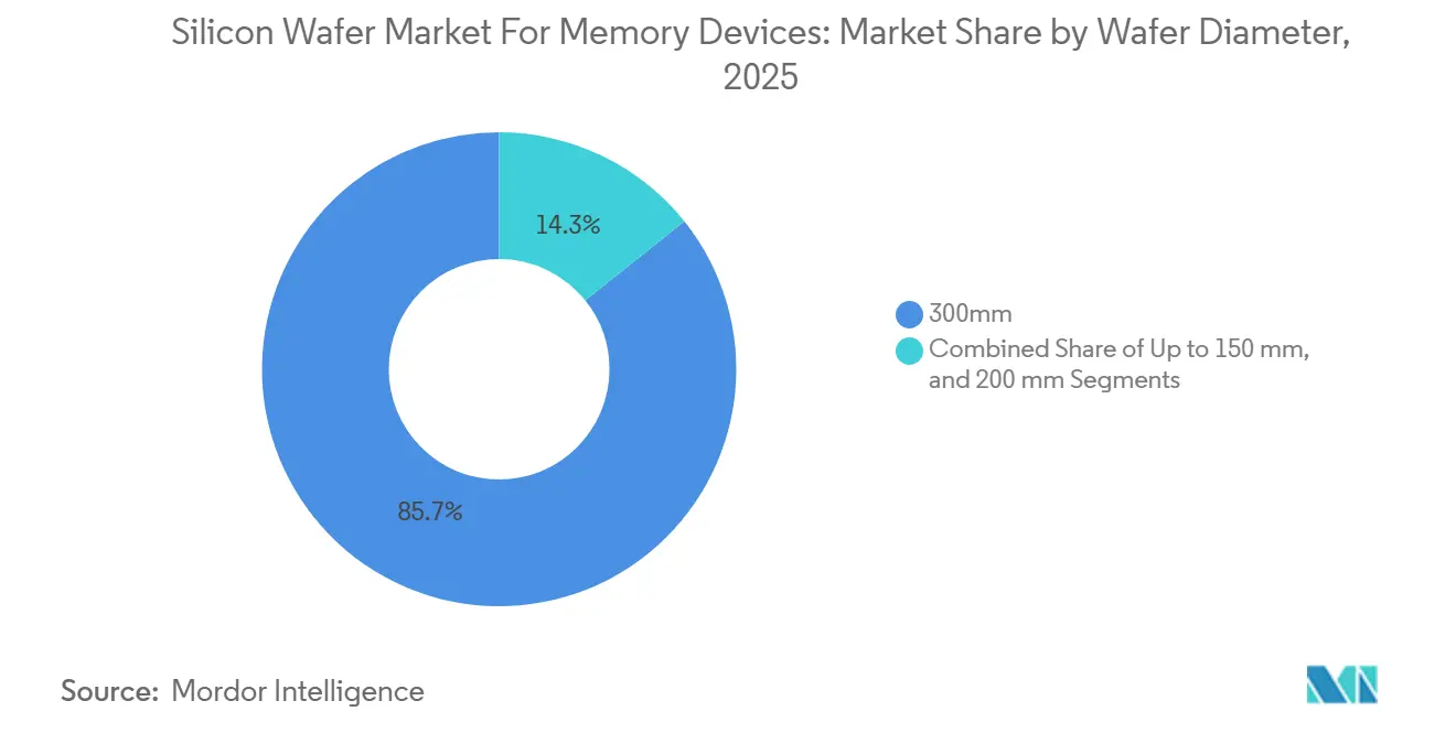
- By wafer diameter, 300 mm captured 85.73% of the silicon wafer market share for memory devices in 2025; it is projected to expand at a 5.11% CAGR through 2031.
- By wafer type, prime polished substrates held 81.22% of 2025 volume, whereas SOI substrates are the fastest mover with a 5.29% CAGR to 2031.
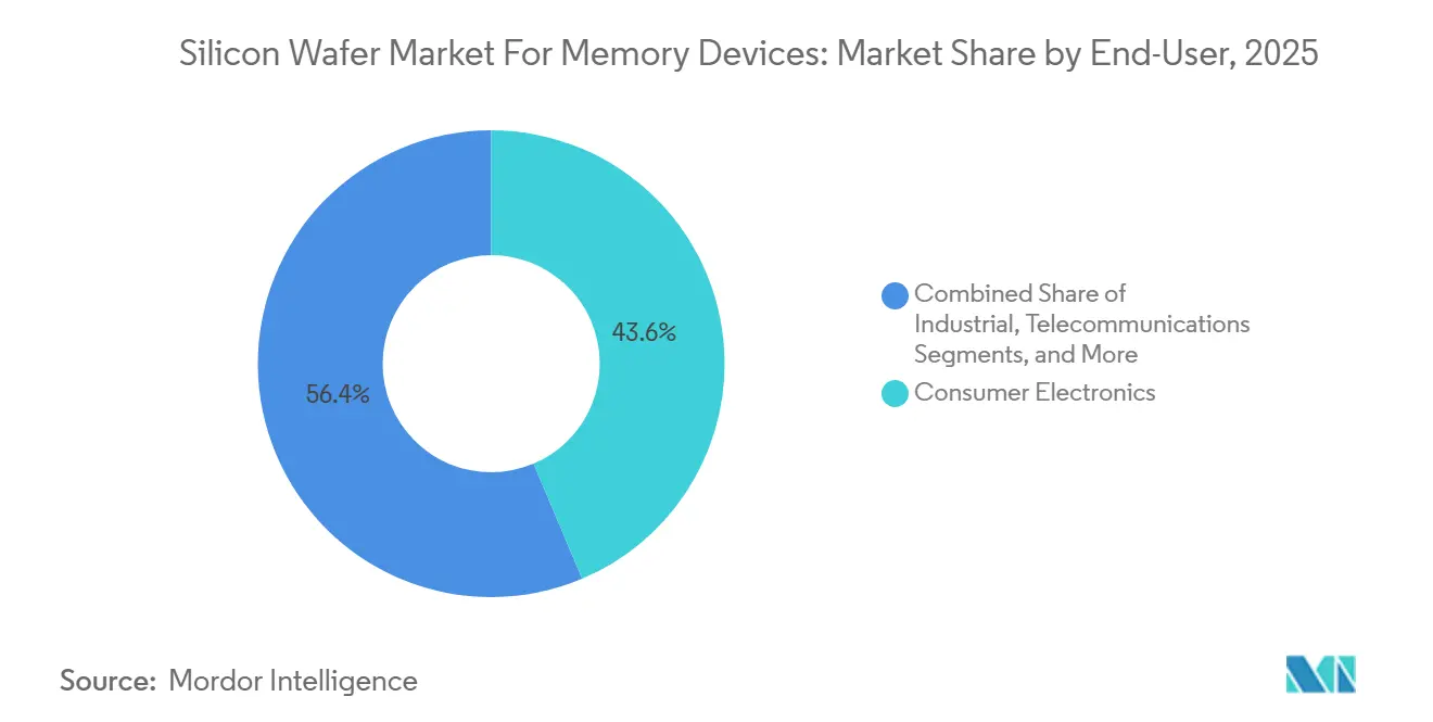
- By end-user, consumer electronics accounted for 43.63% of 2025 demand, while automotive applications exhibit the highest growth at a 4.98% CAGR to 2031.
- By geography, Asia-Pacific dominated with 83.19% share of the silicon wafer market size for memory devices in 2025 and is advancing at a 5.16% CAGR through 2031.
Note: Market size and forecast figures in this report are generated using Mordor Intelligence’s proprietary estimation framework, updated with the latest available data and insights as of January 2026.
Global Silicon Wafer for Memory Devices Market Trends and Insights
Drivers Impact Analysis*
| Driver | (~) % Impact on CAGR Forecast | Geographic Relevance | Impact Timeline |
|---|---|---|---|
| Accelerating Transition to 300 mm Fabs | +1.2% | Taiwan, South Korea, Japan, Global spill-over | Medium term (2-4 years) |
| Expansion of AI-Driven Memory Demand | +1.5% | North America and Asia-Pacific, emerging Europe | Short term (≤ 2 years) |
| Growing Automotive Memory for ADAS and EVs | +0.9% | United States, Germany, Japan, Global | Medium term (2-4 years) |
| Commercialization of 3 D DRAM/NRAM Stacks | +0.7% | South Korea, Taiwan, pilot United States | Long term (≥ 4 years) |
| In-line Laser Anneal Boosting Wafer Yields | +0.4% | Core manufacturing hubs in Asia-Pacific | Medium term (2-4 years) |
| Government CHIPS Incentives | +0.8% | United States, European Union, Japan, India | Long term (≥ 4 years) |
| Source: Mordor Intelligence | |||
Accelerating Transition to 300 mm Fabs
Memory manufacturers are decommissioning 200 mm lines and pouring capital into 300 mm platforms that generate 2.25× more die area per wafer, slicing per-gigabyte substrate cost by roughly 30%. TSMC’s Kumamoto Fab 2 earmarks 300 mm capacity for specialty DRAM aimed at automotive clients, and Samsung plus SK Hynix are repurposing 200 mm facilities into R&D centers to speed next-generation materials work. Advanced nodes for HBM3 E rely on through-silicon vias that remain economical only on 300 mm substrates. Smaller foundries in China and Taiwan are snapping up refurbished 300 mm toolsets to leapfrog export-control hurdles, widening the installed base and underpinning long-term substrate demand. The trend also lets memory IDMs co-locate logic and DRAM on the same diameter, an efficiency play for compute-in-memory architectures.[1]L. Miller, “Compute-in-Memory Architectures,” IEEE Spectrum, spectrum.ieee.org
Expansion of AI-Driven Memory Demand in Data Centers
Generative-AI clusters now absorb HBM stacks that need 40% more wafer area per terabyte than DDR5. SK hynix shipped 12-high HBM3 E in 2Q 2025 and Micron moved to 36 GB stacks in early 2026, both based on 300 mm base wafers featuring fine-pitch copper pillar bumps. Hyperscalers also roll out GDDR7 for inference workloads, creating a dual-track demand curve that rewards wafer vendors who can supply ultra-flat substrates for HBM alongside standard wafers for GDDR7. SEMI projects AI-tied DRAM will hit 28% of total DRAM wafer starts by 2027, double 2024 levels.[2]A. Jones, “AI Memory Demand Forecast,” SEMI, semi.org As GPU memory footprints expand, substrate orders remain resilient even during DRAM pricing dips, cushioning revenue swings for wafer suppliers.
Growing Automotive Memory for ADAS and EV Platforms
Automotive OEMs transition toward LPDDR5 X and UFS 4.0 solutions that demand ASIL-D functional safety. SK hynix secured ASIL-D qualification in March 2025 with wafers exhibiting less than 0.3 µm total-thickness variation, ensuring bond-wire integrity across -40 °C to 125 °C. Zonal compute architectures in EVs now require up to 64 GB DRAM per vehicle, quadrupling memory content relative to internal-combustion models. Tier-1s such as Bosch and Continental co-fund wafer qualification, a new partnership model that improves traceability and lifts process-control costs for substrate vendors. The steady rise of autonomous features keeps wafer demand counter-cyclical to consumer-electronics slowdowns.
Commercialization of 3 D DRAM/NRAM Stacks
Samsung and SK Hynix aim for 16-layer and 24-layer 3 D DRAM in mass production by 2028. Ultra-low defect density requirements prompt wafer makers to invest in atomic-layer deposition to guarantee viable bonding interfaces. Intel and IBM are exploring neuromorphic RAM concepts that embed resistive elements within the substrate, although endurance remains a hurdle. As stacked memory becomes mainstream, wafer suppliers will segment offerings into premium ultra-flat substrates and commodity grades for planar DRAM, each with distinctive pricing and margin structures.
Restraints Impact Analysis*
| Restraint | (~) % Impact on CAGR Forecast | Geographic Relevance | Impact Timeline |
|---|---|---|---|
| Cyclical Cap-Ex Cuts by Memory IDMs | -0.8% | South Korea, Taiwan, Global | Short term (≤ 2 years) |
| Supply Bottlenecks in Polysilicon Feedstock | -0.5% | China, Germany, Global | Medium term (2-4 years) |
| Escalating Energy-Intensity Compliance Costs | -0.3% | European Union, Japan, South Korea | Long term (≥ 4 years) |
| Delayed Qualification of 450 mm Toolsets | -0.2% | United States, Japan, Global | Long term (≥ 4 years) |
| Source: Mordor Intelligence | |||
Cyclical Cap-Ex Cuts by Memory IDMs
Memory producers slashed capital expenditure by USD 12 billion in 2024-2025 amid sub-cash-cost DRAM pricing, postponing new fab ramps and throttling wafer procurement. Samsung deferred its Pyeongtaek P4 expansion, and Micron delayed equipment installs in Idaho and Singapore. Given a 12-18-month wafer production lead time, abrupt order cancellations saddle substrate vendors with excess inventory, eroding margins by up to 300 basis points. Take-or-pay contracts could mitigate risk, but IDMs resist during downturns, prolonging volatility.
Supply Bottlenecks in Polysilicon Feedstock
Solar-sector demand and anti-dumping measures squeezed semiconductor-grade polysilicon in 2025, sending spot prices from USD 28/kg in 2024 to USD 34/kg mid-2025. Hemlock’s USD 325 million CHIPS Act project adds only 8% of global capacity by 2028, and output is ring-fenced for US wafer buyers.[3]US Department of Commerce, “CHIPS Act Funding Announcements,” commerce.gov With China still supplying 60% of high-purity polysilicon, geopolitical shocks could trigger supply interruptions that substrate vendors cannot hedge through alternative sourcing. Longer-term, diversification into fluidized-bed reactor capacity in the United States and Germany may ease shortages, but timelines remain stretched.
*Our forecasts treat driver/restraint impacts as directional, not additive. The impact forecasts reflect baseline growth, mix effects, and variable interactions.
Segment Analysis
By Wafer Diameter: 300 mm Economies Drive Consolidation
The 300 mm slice of the Silicon Wafer for Memory Devices Market commanded 85.73% volume in 2025, and the segment is set to grow at 5.11% CAGR through 2031. That dominance translates into a substantial silicon wafer market size for memory devices at the diameter level, reinforcing supplier focus on ultra-flat polishing and low defect densities. Extreme ultraviolet lithography for sub-10 nm DRAM nodes imposes a total-thickness variation of less than 0.2 µm, a bar that only a few vendors can meet, reinforcing barriers to entry. Commodity 200 mm wafers retain traction for legacy automotive power ICs, yet a mere 2.8% growth rate flags a sunset trajectory as refurbished 300 mm toolsets permeate China and Southeast Asia. Wafers under 150 mm persist in MEMS niches, but their combined share is less than 1.3%, rendering them strategically irrelevant for mainstream memory producers.
Equipment amortization favors 300 mm lines because a single lot delivers 2.25× the die surface area of 200 mm lines without proportionally higher labor or utility costs. TSMC’s choice to dedicate Kumamoto Fab 2 to specialty DRAM shows memory is now vying head-to-head with logic for premium 300 mm capacity. As a result, long-term 300 mm wafer contracts signed in 2025 rose in price by 8-12%. Smaller suppliers either exit or form joint ventures given greenfield fabs cost upward of USD 500 million. Oligopolists leverage scale to invest in through-silicon via ready substrates, locking in future 3 D DRAM opportunities.


By Wafer Type: SOI Gains in Automotive RF
Prime polished substrates delivered 81.22% of volume in 2025, reflecting legacy process compatibility. They continue to anchor the Silicon Wafer for Memory Devices Market market share because consumer DRAM and NAND lines rely on cost-optimized bulk silicon. SOI substrates, however, are expanding at a 5.29% CAGR, outperforming the overall Silicon Wafer for Memory Devices Market. Automotive radar and 5 G RF modules exploit SOI’s lower parasitic capacitance, and Soitec shipped 2 million 300 mm FD-SOI wafers in 2025, illustrating robust end-market pull. Epitaxial wafers, with a 9% share, grow modestly by 4.1% because power-device vendors dabble in GaN-on-Si for EV inverters, an adjacent but not core memory-device field.
SOI uptake is most visible in China, where FD-SOI sidesteps FinFET export constraints. Shanghai Simgui lifted 200 mm SOI output by 25% in 2025 to feed domestic RF manufacturers. Specialty substrates segment the value chain into high-margin, lower-volume pockets versus commoditized prime polished wafers. The 3.7-percentage-point growth differential underscores that specialty spaces will capture incremental profits even if prime polished remains numerically dominant through 2031.
By End-User: Automotive Closes Gap with Consumer Electronics
Consumer electronics consumed 43.63% of wafers in 2025, underpinned by smartphone and PC memory refreshes. Yet its 3.9% trajectory lags the 4.98% CAGR posted by automotive. EV platforms featuring centralized compute demand up to 64 GB DRAM per vehicle, multiplying substrate pull even while global auto unit sales stagnate. The silicon wafer market size for memory devices linked to automotive use is therefore expanding faster than handset-driven demand. Industrial automation shows 4.2% growth, boosted by collaborative robots deploying LPDDR4 X, whereas telecom infrastructure’s 4.5% ramp leverages GDDR6 in 5 G base stations. Medical and aerospace remain steady at 3.5% because qualification cycles deter rapid technology refresh.
Tier-1 automotive suppliers co-invest in wafer-spec definition, a stark contrast with consumer electronics where IDMs dictate standards. This alignment raises the silicon wafer market share for memory devices supplied into vehicles, narrowing the divide with smartphones. The dual-market exposure, however, synchronizes risk; if both sectors soften simultaneously, wafer demand could dip sharply, emphasizing the importance of geographic and product diversification for substrate makers.
Geography Analysis
Asia-Pacific dominated the Silicon Wafer for Memory Devices Market with 83.19% production volume in 2025, growing at 5.16% CAGR to 2031. South Korea’s vertically integrated complexes in Pyeongtaek and Icheon shave substrate lead times from 18 to 12 months, yielding valuable yield-feedback loops. Taiwan’s ecosystem benefits from TSMC-Sony-Denso’s Kumamoto venture, which channels Japanese subsidies worth JPY 476 billion (USD 3.2 billion) to localize DRAM wafers. China’s 18% slice within Asia-Pacific, led by Shanghai Simgui and GRINM, is still reliant on imported polysilicon and crystal-pulling tools, keeping the door open for export-control disruptions.
North America accounted for 9% of 2025 volume, lifted by CHIPS Act grants. GlobalWafers’ Sherman plant will add 1.2 million 300 mm wafers annually by 2028, reducing U.S. dependence on imports. Europe’s 4% share inches ahead at a 4.3% pace thanks to EUR 43 billion (USD 46 billion) in Chips Act incentives supporting Infineon and STMicroelectronics expansions. Still, supply remains fragmented, with Siltronic spanning Germany and Singapore, limiting scale-related cost advantages. South America and the Middle East and Africa together remain below 1%, lacking indigenous memory fabs and facing steep capital-barrier hurdles.
The Silicon Wafer for Memory Devices Market therefore clusters around three manufacturing zones, East Asia mega-fabs, North American sovereign capacity, and Europe’s mid-scale specialty lines. Policymakers push for local resilience, but raw-material concentration and tooling dependencies mean genuine self-sufficiency is years away. For suppliers, this geography mix implies juggling multiple compliance regimes while ensuring just-in-time delivery over an increasingly regionalized logistics map.

Competitive Landscape
Shin-Etsu Chemical, SUMCO Corporation, and GlobalWafers collectively controlled roughly 65% of 300 mm prime polished capacity in 2025, giving the Silicon Wafer for Memory Devices Market a moderately concentrated profile. Historical price discipline rested on synchronized capacity adds, but the Texas and Singapore expansions by GlobalWafers and Siltronic inject fresh output that could trim operating margins by 150-200 basis points if demand underperforms projections. Commodity suppliers now compete on cycle time and yield, whereas Soitec and Okmetic pursue high-margin niches like FD-SOI and high-resistivity substrates.
Patent filings for wafer-level packaging climbed 22% in 2025, signaling a pivot upstream into silicon interposers where gross margins run 20-30% above bare wafers.[4]IEEE Conference Proceedings, “Wafer-Level Packaging Trends,” IEEE Xplore, ieeexplore.ieee.org Smaller firms such as Wafer Works and Zing Semiconductor forge co-development pacts with IDMs on hybrid-bonding processes essential for 3D DRAM stacking. The move reflects an industry consensus that margin pools are migrating from substrate supply toward integration and packaging services.
Concurrently, energy-intensity regulations and carbon tariffs in Europe raise operating-cost differentials that favor locations with low-carbon power grids. Competitive behavior is thus shaped by capacity timing, upstream diversification, and compliance agility rather than by simple scale economics alone.
Silicon Wafer for Memory Devices Industry Leaders
Shin-Etsu Chemical Co Ltd
SUMCO Corporation
GlobalWafers Co Ltd
Siltronic AG
SK siltron Co Ltd
- *Disclaimer: Major Players sorted in no particular order

Recent Industry Developments
- February 2026: GlobalWafers won final approval for USD 400 million CHIPS Act funding to build a 300 mm wafer plant in Sherman, Texas, with production slated for late 2027.
- January 2026: SK hynix ramped mass production of 12-high HBM3 E stacks at its Icheon M16 fab, supplying NVIDIA’s H200 GPUs.
- December 2025: Soitec and STMicroelectronics signed a joint program to scale 22 nm FD-SOI wafer output for automotive radar, with pilot runs due mid-2026.
- November 2025: Micron began volume shipments of HBM3 E Gen2 memory, using 300 mm wafers with hybrid bonding for 36 GB stacks.


Global Silicon Wafer for Memory Devices Market Report Scope
The Silicon Wafer for Memory Devices Market is witnessing significant growth, driven by increasing demand for advanced memory solutions across various industries. The adoption of silicon wafers in applications such as consumer electronics, automotive, and telecommunications is expanding due to their critical role in enhancing device performance and efficiency.
The Silicon Wafer for Memory Devices Market Report is Segmented by Wafer Diameter (Up to 150mm, 200mm, 300mm), Wafer Type (Prime Polished, Epitaxial, Silicon-on-Insulator, Specialty Silicon), End-user (Consumer Electronics, Industrial, Telecommunications, Automotive, Other Applications), and Geography (North America, Europe, Asia-Pacific, South America, Middle East and Africa). Market Forecasts are Provided in Terms of Volume (Square Inches).
| Up to 150 mm |
| 200 mm |
| 300 mm |
| Prime Polished |
| Epitaxial |
| Silicon-on-Insulator (SOI) |
| Specialty Silicon (High-Resistivity, Power, Sensor-Grade) |
| Consumer Electronics | Mobile and Smartphones |
| PCs and Servers | |
| Industrial | |
| Telecommunications | |
| Automotive | |
| Other End-user Applications |
| North America | United States |
| Canada | |
| Mexico | |
| Europe | Germany |
| United Kingdom | |
| France | |
| Rest of Europe | |
| Asia-Pacific | China |
| Japan | |
| India | |
| South Korea | |
| Taiwan | |
| Rest of Asia-Pacific | |
| South America | |
| Middle East and Africa |
| By Wafer Diameter | Up to 150 mm | |
| 200 mm | ||
| 300 mm | ||
| By Wafer Type | Prime Polished | |
| Epitaxial | ||
| Silicon-on-Insulator (SOI) | ||
| Specialty Silicon (High-Resistivity, Power, Sensor-Grade) | ||
| By End-user | Consumer Electronics | Mobile and Smartphones |
| PCs and Servers | ||
| Industrial | ||
| Telecommunications | ||
| Automotive | ||
| Other End-user Applications | ||
| By Geography | North America | United States |
| Canada | ||
| Mexico | ||
| Europe | Germany | |
| United Kingdom | ||
| France | ||
| Rest of Europe | ||
| Asia-Pacific | China | |
| Japan | ||
| India | ||
| South Korea | ||
| Taiwan | ||
| Rest of Asia-Pacific | ||
| South America | ||
| Middle East and Africa | ||


Key Questions Answered in the Report
What is the projected volume for 300 mm wafers dedicated to memory by 2031?
The 300 mm segment of the Silicon Wafer for Memory Devices Market is forecast to reach roughly 4.3 billion square inches by 2031, reflecting a 5.11% CAGR from 2026.
Why are SOI wafers gaining traction in automotive applications?
SOI substrates cut parasitic capacitance, improving millimeter-wave signal integrity for radar and RF front-ends, and their uptake is accelerating at a 5.29% CAGR within automotive memory lines.
How do CHIPS Act incentives influence U.S. wafer supply?
Grants have funded GlobalWafers’ Texas fab and Hemlock’s polysilicon expansion, collectively adding domestic wafer and feedstock capacity that lowers import dependence.
Which regions hold the largest share of wafer production for memory devices?
Asia-Pacific retains 83.19% of volume, led by South Korea, Taiwan, Japan, and China, with North America and Europe together below 13%.
What are the main cost pressures facing wafer suppliers?
Volatile polysilicon pricing, energy-intensity compliance in the European Union, and IDM cap-ex cycles exert downward margin pressure despite steady long-term demand.
How is advanced packaging altering wafer-supplier strategies?
Vendors increasingly invest in silicon interposers and through-silicon via services, chasing margins 20-30% higher than bare-wafer sales and differentiating via intellectual property.
How large will Silicon Wafer for Memory Devices Market by 2031?
The Silicon Wafer for Memory Devices Market size is forecast to reach 5.03 billion square inches by 2031 at a 4.72% CAGR.
Page last updated on:


