Size and Share of Silicon Wafer Market For Analog ICs
Market Overview
| Study Period | 2020 - 2031 |
|---|---|
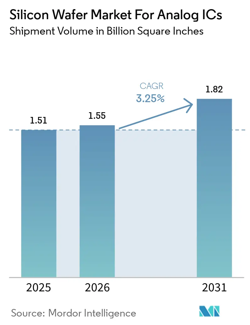
| Market Volume (2026) | 1.55 Billion Square Inches |
| Market Volume (2031) | 1.82 Billion Square Inches |
| Growth Rate (2026 - 2031) | 3.25% CAGR |
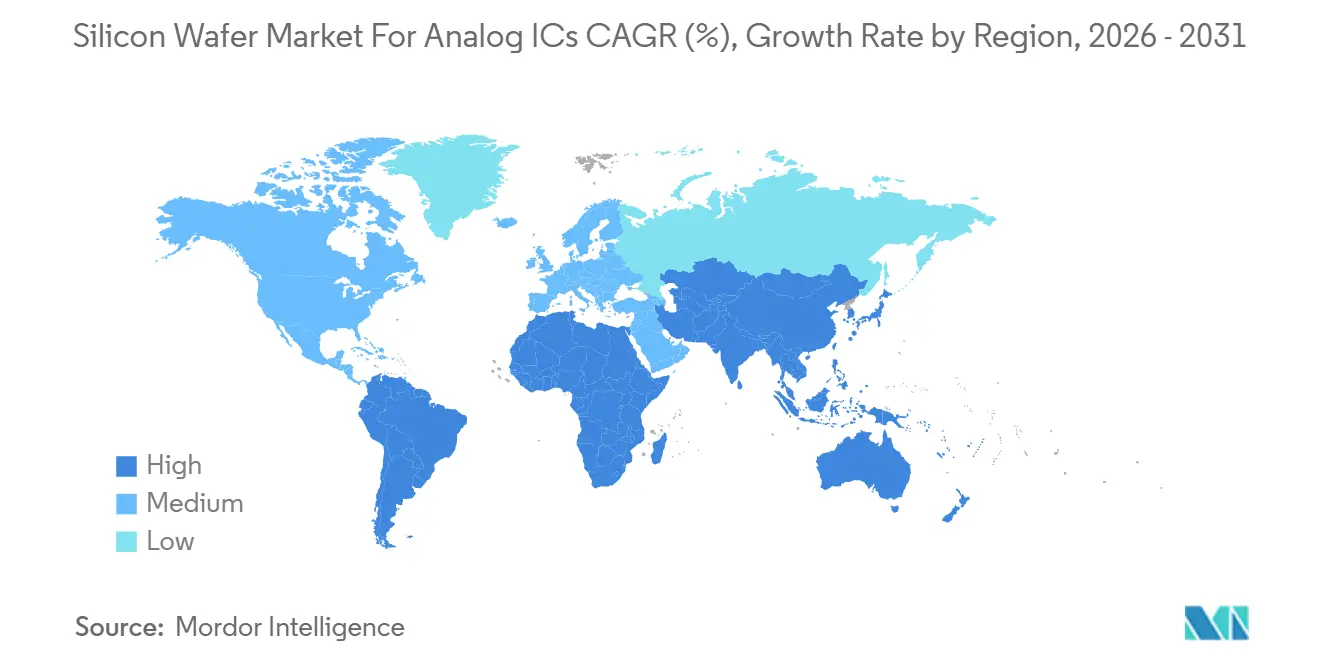
| Fastest Growing Market | Asia Pacific |
| Largest Market | Asia Pacific |
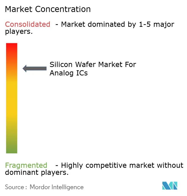
| Market Concentration | High |
Major Players *Disclaimer: Major Players sorted in no particular order Image © Mordor Intelligence. Reuse requires attribution under CC BY 4.0. | |
Analysis of Silicon Wafer Market For Analog ICs by Mordor Intelligence
The silicon wafer market for analog ICs industry size in terms of shipment volume is projected to be 1.51 Billion Square Inches in 2025, 1.55 Billion Square Inches in 2026, and reach 1.82 Billion Square Inches by 2031, growing at a CAGR of 3.25% from 2026 to 2031. Structural shifts toward automotive electrification, AI datacenter power delivery, and industrial automation are redirecting capacity from consumer electronics to high-reliability applications. Mature 200 mm nodes still dominate volume, yet 300 mm tools are gaining momentum as suppliers target 30%-40% die-cost reductions for high-voltage PMICs. Investments from GlobalWafers, Texas Instruments, and Siltronic are accelerating 300 mm output, while CHIPS and EU Chips incentives foster regional diversification. Sustainability mandates around water and energy usage, combined with persistent polysilicon tightness, keep pricing power in the hands of vertically integrated incumbents.
Key Report Takeaways
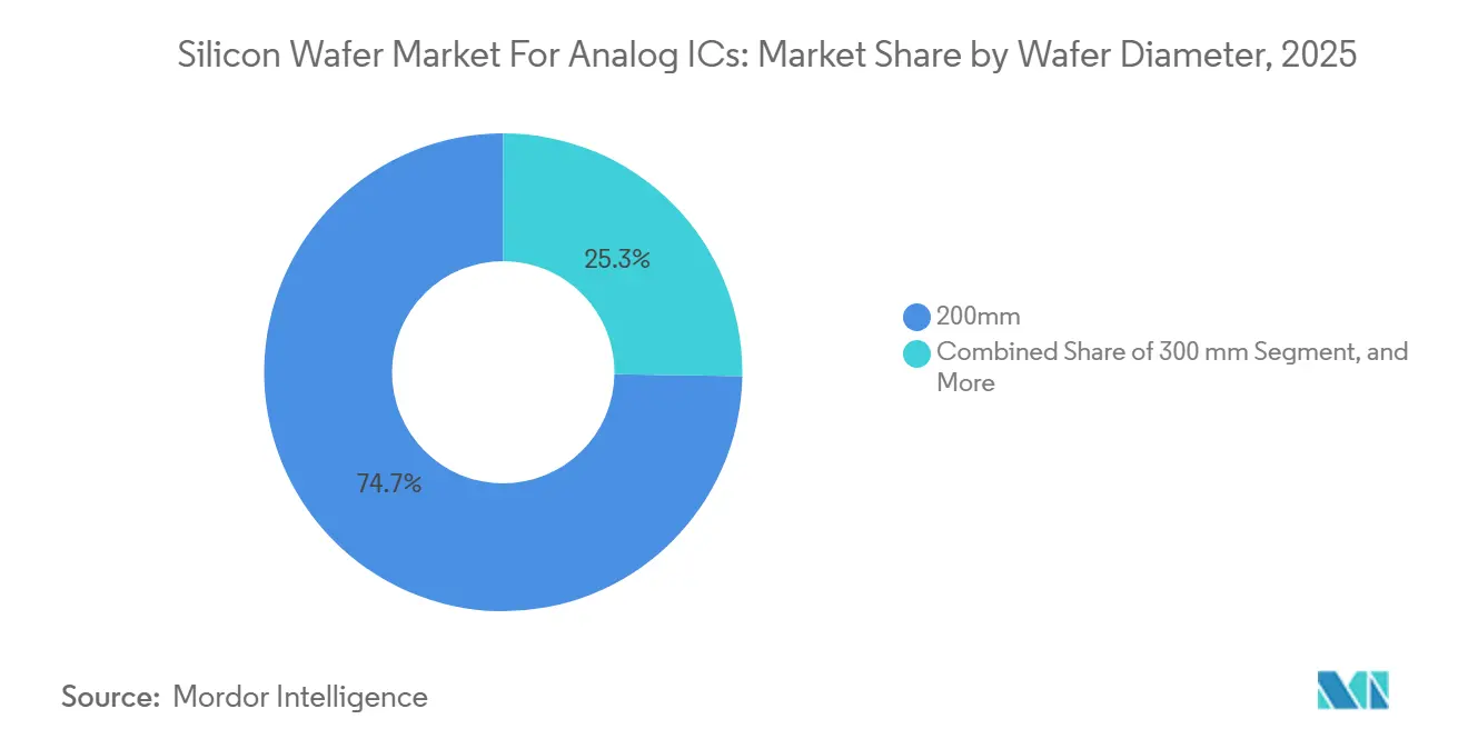
- By wafer diameter, the 200 mm segment led with 74.74% of the silicon wafer market for analog ICs market share in 2025, whereas 300 mm substrates are forecast to post the fastest 3.89% CAGR to 2031.
- By wafer type, prime polished held a 47.64% of the silicon wafer market for analog ICs market share in 2025, while specialty silicon is advancing at a 3.95% CAGR through 2031.
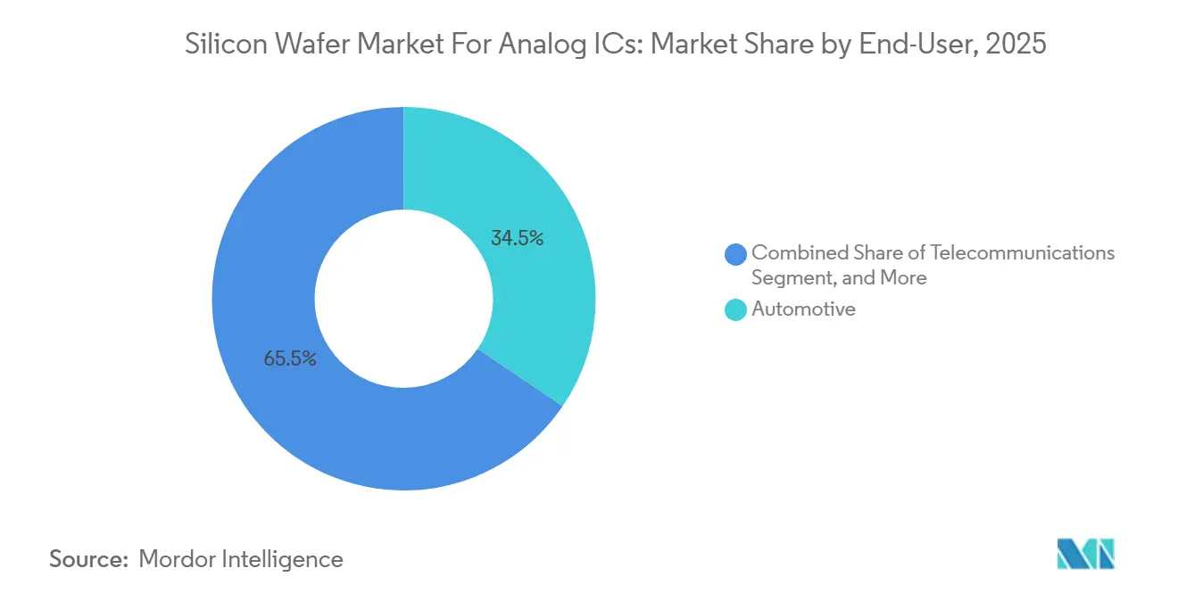
- By end-user, automotive applications accounted for 34.48% of 2025 volume and are projected to grow at a 4.11% CAGR through 2031.
- By geography, Asia-Pacific accounted for 67.77% of 2025 shipments and is set to expand at a 4.06% CAGR over the same horizon.
Note: Market size and forecast figures in this report are generated using Mordor Intelligence’s proprietary estimation framework, updated with the latest available data and insights as of January 2026.
Insights and Trends of Silicon Wafer Market For Analog ICs
Drivers Impact Analysis*
| Driver | (~) % Impact on CAGR Forecast | Geographic Relevance | Impact Timeline |
|---|---|---|---|
| Capacity Expansion by 300mm Foundries for Power-Efficient Analog ICs | +1.2% | Global, with concentration in Taiwan, United States, Germany | Medium term (2-4 years) |
| Growing Demand for High-Voltage PMICs in EV Fast-Charging | +0.9% | Global, led by China, Europe, North America | Medium term (2-4 years) |
| Analog Front-End Integration in 5G Massive-MIMO Radios | +0.6% | Asia-Pacific core, spillover to Middle East and Africa | Short term (≤ 2 years) |
| Transition to Wide-Bandgap Gate Drivers Requiring Ultra-Low Defect Wafers | +0.5% | North America and Europe, early adoption in automotive hubs | Long term (≥ 4 years) |
| On-shoring Incentives under CHIPS and EU Chips Acts | +0.7% | North America and Europe | Medium term (2-4 years) |
| Adoption of AI-Based Process Control Reducing Scrap Rates | +0.4% | Global, with early deployment in leading-edge fabs | Short term (≤ 2 years) |
| Source: Mordor Intelligence | |||
Capacity Expansion by 300 mm Foundries for Power-Efficient Analog ICs
Foundries are channeling multi-billion-dollar outlays into 300 mm lines targeting analog nodes above 28 nm, because larger wafers trim die costs even when yields lag those of leading-edge logic. GlobalWafers’ USD 7.5 billion Texas project and Siltronic’s EUR 2 billion German-Singapore plan illustrate the scale of this pivot. Texas Instruments is replicating the model in Richardson and Lehi, using CHIPS grants to offset the capital intensity. SEMI forecasts that analog, power, and discrete fabs will absorb more than USD 41 billion in equipment from 2026-2028.[1]Semiconductor Equipment and Materials International, “Global Fab Equipment Outlook 2026-2028,” semi.org These investments position the silicon wafer market for analog ICs to shift its center of gravity toward 300 mm production by the end of the decade.
Growing Demand for High-Voltage PMICs in EV Fast-Charging
Fast-charging systems operating above 800 V require epitaxial silicon wafers with defect densities below 0.05 cm-² to prevent catastrophic breakdown. Renesas, Analog Devices, and NXP have all introduced PMICs rated 42 V-60 V that meet ISO 26262 safety levels. The International Energy Agency expects EV sales to exceed 17 million units in 2025, amplifying substrate demand tied to 350 kW chargers.[2]International Energy Agency, “Global EV Outlook 2025,” iea.org Specialty silicon suppliers that can guarantee tight control of resistivity are therefore securing long-term supply contracts with automotive IDMs.
Analog Front-End Integration in 5G Massive-MIMO Radios
5G operators are rolling out massive-MIMO arrays that integrate power amplifiers, transceivers, and beamformers on RF-SOI or GaN-on-Si substrates to curb tower power draw.[3]Analog Devices, “MAX20057 Data Sheet,” analog.com Qorvo sources RF-SOI wafers from Soitec with quality factors above 40 at C-band. Imec has demonstrated GaN-on-Si PAs hitting 45% efficiency at 28 GHz. The silicon wafer market for analog ICs thus benefits from elevated flatness and resistivity targets that only premium substrates deliver.
Transition to Wide-Bandgap Gate Drivers Requiring Ultra-Low Defect Wafers
SiC and GaN power stages demand silicon-gate driver ICs capable of switching beyond 100 kHz without shoot-through, requiring oxygen concentrations below 5 ppb and total-thickness variation below 0.5 µm. Toshiba’s partnership with Shanghai Simgui on 200 mm SiC emphasizes the role of hybrid supply chains. STMicroelectronics plans to triple SiC epitaxy in Catania by 2027, spotlighting how specialty silicon anchors the transition to electrified transport.
Restraints Impact Analysis*
| Restraint | (~) % Impact on CAGR Forecast | Geographic Relevance | Impact Timeline |
|---|---|---|---|
| Cyclical Capital Expenditure of Analog IDMs | -0.8% | Global, pronounced in North America and Europe | Short term (≤ 2 years) |
| Supply Tightness of High-Purity Polysilicon Feedstock | -0.6% | Global, with acute impact in Asia-Pacific | Medium term (2-4 years) |
| Yield Challenges in ≥200mm SOI Wafers for mmWave RF | -0.4% | Global, concentrated in North America and Europe | Long term (≥ 4 years) |
| Sustainability Pressures on Water and Energy Usage | -0.5% | Global, regulatory focus in Europe and California | Medium term (2-4 years) |
| Source: Mordor Intelligence | |||
Cyclical Capital Expenditure of Analog IDMs
Automotive and industrial customers adjust orders quickly, forcing analog IDMs to throttle fab utilization. Shin-Etsu Chemical reported softer 200 mm volumes after automotive inventory corrections in October 2025. In its 2024 filings, Texas Instruments announced the postponement of its tool installations. These cyclical delays exert downward pressure on wafer Average Selling Prices (ASPs) and significantly increase the risks associated with working capital for suppliers.
Supply Tightness of High-Purity Polysilicon Feedstock
Polysilicon prices rose from USD 20/kg to USD 28/kg between 2024-2025 as solar demand outpaced reactor expansions. Wacker's Burghausen project, with an investment of EUR 2.5 billion, is projected to reach its full operational capacity only by late 2026. The ongoing high-purity deficits are contributing to cost inflation within the silicon wafer market for analog integrated circuits (ICs). This situation is creating significant advantages for vendors that possess captive feedstock operations, enabling them to mitigate supply chain challenges and capitalize on the prevailing market conditions.
*Our forecasts treat driver/restraint impacts as directional, not additive. The impact forecasts reflect baseline growth, mix effects, and variable interactions.
Segment Analysis
By Wafer Diameter: 300 mm Accelerates Cost-Down Momentum
The 200 mm class captured 74.74% of the analog ICs silicon wafer market share in 2025. However, the 300 mm category is on track for a 3.89% CAGR to 2031 as Texas Instruments and GlobalWafers qualify power-efficient analog flows on larger substrates. Fab conversions exploit common lithography footprints, allowing analog IDMs to slice 30%-40% from die cost without node shrinks. Early adopters focus on PMICs and data-converter families whose layouts tolerate relaxed design rules, ensuring quick returns on 300 mm capex.
A residual niche of up to 150 mm persists for high-voltage thyristors and R&D pilots, but will continue to contract as equipment makers extend their toolsets to 200 mm refurb lines. Meanwhile, 200 mm capacity remains constrained; inventory swings in automotive cause short-term softness, yet industrial robot and renewable-energy demand continue to absorb mature-node supply. Over the forecast, rising 300 mm availability will rebalance the diameter mix, nudging the silicon wafer market for analog ICs toward a more diversified cost base.


By Wafer Type: Specialty Grades Outpace Commodity Supply
Prime polished substrates held 47.64% share in 2025, reflecting their role in mainstream bipolar-CMOS-DMOS flows. Specialty silicon is forecast to outgrow the overall silicon wafer market for analog ICs at a 3.95% CAGR, driven by RF-SOI, high-resistivity float-zone, and sensor-grade wafers. RF switch designers prize SOI structures for their low parasitics, while MEMS suppliers demand oxygen levels below 5 ppb to curb drift.
Epitaxial wafers underpin automotive PMICs and industrial drives where precise doping sustains breakdown voltages. STMicroelectronics is vertically integrating SiC epitaxy to lock in supply. Cost remains the chief adoption barrier for SOI, as buried-oxide fabrication can multiply wafer costs by 10. Nonetheless, where millimeter-wave isolation or wide-bandgap control loops dictate ultra-clean substrates, specialty silicon’s value proposition outweighs price sensitivity, reinforcing high-margin niches inside the silicon wafer market for analog ICs.
By End-User: Automotive Electrification Leads Growth
Automotive captured 34.48% of the analog ICs silicon wafer market in 2025 and is projected to grow at a 4.11% CAGR through 2031. Electric vehicle (EV) traction inverters, on-board chargers, and advanced driver-assistance system (ADAS) sensors collectively result in a twofold increase in analog content per vehicle when compared to their internal-combustion engine predecessors. Consequently, the demand for wafer call-offs has been rising, driven by the adoption of ISO 26262-compliant power management integrated circuits (PMICs) and sensor conditioners, despite the cyclical fluctuations in original equipment manufacturer (OEM) production.
Consumer electronics still consume large volumes of LDOs, codecs, and haptic drivers, but lengthening smartphone replacement cycles are tempering wafer growth. Industrial automation and renewable-energy inverters turn to robust BC-DMOS flows on 200 mm and 300 mm lines, sustaining steady substrate demand. Telecommunications infrastructure remains a premium segment for RF-SOI and GaN-on-Si wafers that feed 5G macro-cells and small-cells, anchoring high ASPs inside the silicon wafer market for analog ICs.
Geography Analysis
Asia-Pacific commanded 67.77% of 2025 shipments, giving the region the largest share of the analog ICs silicon wafer market and a leading 4.06% CAGR through 2031. Capacity additions by Taiwan Semiconductor Manufacturing Company, Simgui, and SK Siltron are concentrated on 300 mm lines that support high-voltage PMICs and millimeter-wave RF chips. China’s drive for domestic sourcing keeps demand resilient even when global cycles soften, while Japan’s Rapidus project anchors a parallel push into mixed-signal nodes. Korea benefits from proximity to automotive electronics exporters that require mature-node reliability. The region’s tight cluster of fabs and materials vendors shortens logistics cycles and reinforces its cost advantage.
North America held a mid-teens share in 2025 and is growing faster than the global average as CHIPS Act incentives de-risk new analog capacity. GlobalWafers, Texas Instruments, and Onsemi are building or expanding 300 mm plants that collectively aim to reach more than 1 million wafers per month by the late 2020s. Automotive, defense, and datacenter customers prefer domestic sourcing to hedge geopolitical risk and shorten qualification loops. These trends improve utilization of existing 200 mm lines while underpinning financing for new greenfield sites.
Europe maintained a low-double-digit share, helped by EU Chips Act subsidies supporting Infineon, STMicroelectronics, and GlobalFoundries' expansions. Germany’s Dresden hub is emerging as a center for automotive-grade mixed-signal production, while Italy’s Catania facility focuses on silicon-carbide epitaxy. The United Kingdom and France contribute specialty output for RF-SOI and sensor-grade wafers, yet rely on imports for prime polished volume. South America, the Middle East, and Africa together remain below a 5% share, though renewable-energy and telecom projects are creating niche demand that may invite local polishing or slicing operations later in the decade.

Competitive Landscape
The competitive field is moderately concentrated, with Shin-Etsu Chemical, SUMCO Corporation, and GlobalWafers together controlling roughly two-thirds of prime polished and epitaxial capacity. Shin-Etsu’s integration from polysilicon refining to final polish supports price leadership, while SUMCO’s Japan–Taiwan footprint offers supply-chain redundancy valued by automotive IDMs. GlobalWafers is expanding its network with the new Texas megafab, positioning itself closer to North American customers without sacrificing Asian-scale economics. Collectively, the three firms set baseline pricing for commodity grades and influence long-term supply agreements across regions.
Specialty substrates dilute concentration and raise competitive intensity. Soitec dominates silicon-on-insulator for 5G radios, but Okmetic, Siltronix, and Topsil split high-resistivity float-zone and sensor-grade demand. Chinese entrants such as Simgui and Grinm are using state support to break into 200 mm and 300 mm epitaxial supply, adding downward pressure on price even as qualification cycles remain lengthy. Smaller European suppliers carve out niches in ultra-flat wafers for optical sensors, while U.S. startups focus on defect-density improvements tailored to wide-bandgap gate drivers.
Strategic themes revolve around vertical control, AI-enabled yield management, and subsidy capture. Multiple top-tier players are locking up polysilicon feedstock to shield margins from raw-material price swings. Applied Materials’ AIx suite is now standard across many polishing and epitaxy lines, cutting scrap rates and widening the cost gap between leaders and late adopters. Firms are also distributing capacity across continents to tap CHIPS and EU Chips incentives and to serve customers that demand dual sourcing. As sustainability metrics tighten, incumbents that can pair low-defect performance with water-reuse and energy-recovery systems gain a reputational edge that is beginning to influence sourcing decisions.
Leaders of Silicon Wafer Market For Analog ICs
Shin-Etsu Chemical Co., Ltd.
SUMCO Corporation
GlobalWafers Co., Ltd.
Siltronic AG
SK Siltron Co., Ltd.
- *Disclaimer: Major Players sorted in no particular order

Recent Industry Developments
- March 2026: ams-OSRAM closed the sale of its non-optical analog and mixed-signal sensor unit to Infineon for EUR 570 million (USD 638 million).
- January 2026: Shin-Etsu Chemical finished construction of a JPY 83 billion (USD 570 million) lithography-materials plant in Isesaki, Japan.
- December 2025: TSMC unveiled plans to double 300 mm analog capacity to 34 million wafers annually by the mid-2030s with USD 165 billion U.S. investments.
- October 2025: Shin-Etsu Chemical reported flat 300 mm shipments but softer 200 mm volumes amid automotive inventory corrections.


Scope of Report on Silicon Wafer Market For Analog ICs
The Silicon Wafer Market for Analog ICs Report is Segmented by Wafer Diameter (Up to 150 mm, 200 mm, 300 mm), Wafer Type (Prime Polished, Epitaxial, Silicon-on-Insulator, Specialty Silicon), End-user (Consumer Electronics, Industrial, Telecommunications, Automotive, Other End-user Applications), and Geography (North America, Europe, Asia-Pacific, South America, Middle East, Africa). The Market Forecasts are Provided in Terms of Shipment Volume (Square Inches).
| Up to 150 mm |
| 200 mm |
| 300 mm |
| Prime Polished |
| Epitaxial |
| Silicon-on-Insulator (SOI) |
| Specialty Silicon (High-Resistivity, Power, Sensor-Grade) |
| Consumer Electronics | Mobile and Smartphones |
| PCs and Servers | |
| Industrial | |
| Telecommunications | |
| Automotive | |
| Other End-user Applications |
| North America | United States |
| Canada | |
| Mexico | |
| Europe | Germany |
| United Kingdom | |
| France | |
| Rest of Europe | |
| Asia-Pacific | China |
| Japan | |
| India | |
| South Korea | |
| Taiwan | |
| Rest of Asia-Pacific | |
| South America | |
| Middle East | |
| Africa |
| By Wafer Diameter | Up to 150 mm | |
| 200 mm | ||
| 300 mm | ||
| By Wafer Type | Prime Polished | |
| Epitaxial | ||
| Silicon-on-Insulator (SOI) | ||
| Specialty Silicon (High-Resistivity, Power, Sensor-Grade) | ||
| By End-user | Consumer Electronics | Mobile and Smartphones |
| PCs and Servers | ||
| Industrial | ||
| Telecommunications | ||
| Automotive | ||
| Other End-user Applications | ||
| By Geography | North America | United States |
| Canada | ||
| Mexico | ||
| Europe | Germany | |
| United Kingdom | ||
| France | ||
| Rest of Europe | ||
| Asia-Pacific | China | |
| Japan | ||
| India | ||
| South Korea | ||
| Taiwan | ||
| Rest of Asia-Pacific | ||
| South America | ||
| Middle East | ||
| Africa | ||


Key Questions Answered in the Report
How large is the silicon wafer market for analog ICs in 2026?
It is expected to reach 1,555.17 million square inches in 2026, following 5.8% year-on-year shipment growth logged in 2025.
What CAGR will analog IC wafers record through 2031?
The silicon wafer market for analog ICs is projected to grow at a 3.25% CAGR between 2026-2031.
Which wafer diameter is expanding fastest?
300 mm substrates show the strongest momentum, advancing at 3.89% CAGR as analog IDMs migrate cost-sensitive PMIC flows to larger formats.
Why does automotive electrification matter to wafer demand?
EV fast-charging, traction inverters, and ADAS sensors boost analog IC content per vehicle, lifting automotive wafer volume at a 4.11% CAGR through 2031.
Which regions dominate supply?
Asia-Pacific supplies more than two-thirds of analog IC wafers today, though North American and European output is rising under CHIPS-related incentives.
Who are the leading wafer suppliers?
Shin-Etsu Chemical, SUMCO Corporation, and GlobalWafers collectively hold about 66% of prime polished and epitaxial capacity, shaping global pricing dynamics.
Page last updated on:


