Semiconductor Wafer Reclaim Market Size and Share
Market Overview
| Study Period | 2020 - 2031 |
|---|---|
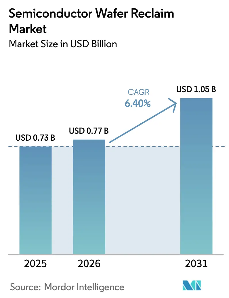
| Market Size (2026) | USD 0.77 Billion |
| Market Size (2031) | USD 1.05 Billion |
| Growth Rate (2026 - 2031) | 6.40% CAGR |
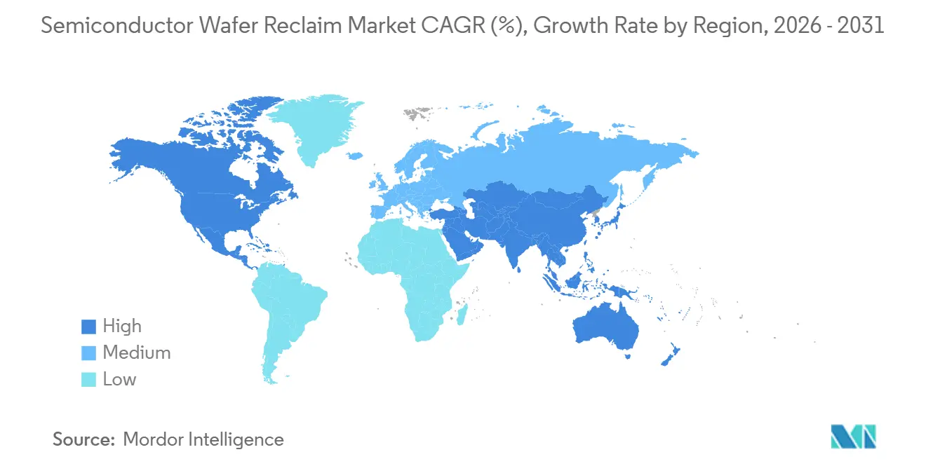
| Fastest Growing Market | Asia Pacific |
| Largest Market | Asia Pacific |
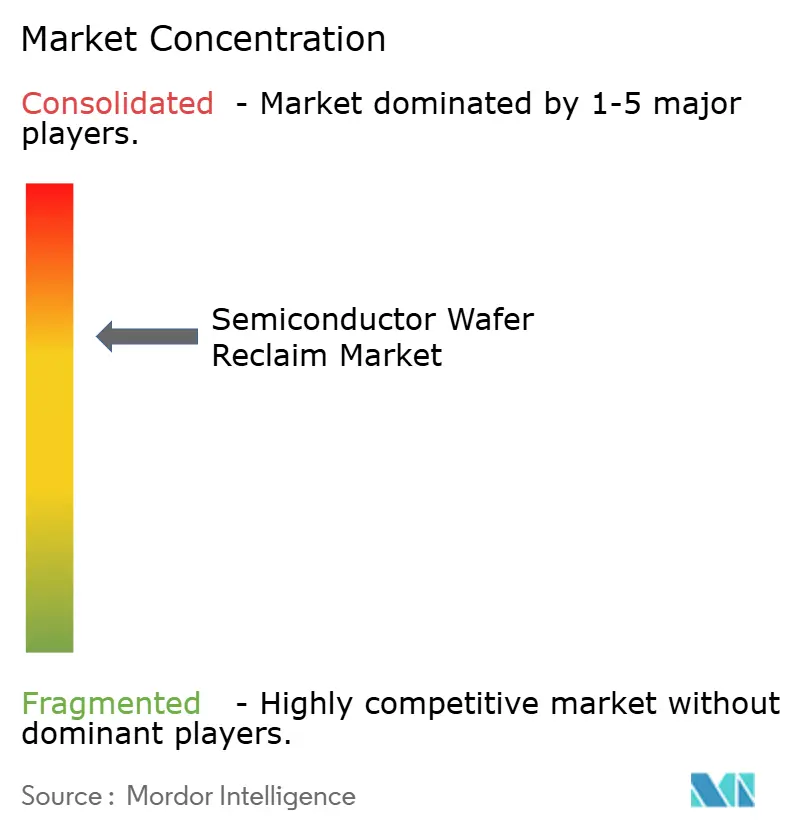
| Market Concentration | Medium |
Major Players *Disclaimer: Major Players sorted in no particular order Image © Mordor Intelligence. Reuse requires attribution under CC BY 4.0. | |
Semiconductor Wafer Reclaim Market Analysis by Mordor Intelligence
The semiconductor wafer reclaim market size was valued at USD 0.73 billion in 2025 and estimated to grow from USD 0.77 billion in 2026 to reach USD 1.05 billion by 2031, at a CAGR of 6.4% during the forecast period (2026-2031). Heightened capital intensity at advanced nodes, paired with regulatory requirements for circular manufacturing, is steering integrated device manufacturers toward reclaimed substrates. The shift lowers total cost of ownership for test and monitor wafers, trims carbon footprints, and buffers supply-chain risk as virgin-wafer pricing stays volatile. Artificial-intelligence-driven inspection now compresses turnaround from days to hours, letting reclaim vendors match the cadence of high-volume fabs. Meanwhile, Asia-Pacific’s dense 300 mm fab cluster anchors demand, while emerging silicon-carbide and gallium-nitride pilot lines open white-space opportunities in compound-semiconductor reclaim. Competitive intensity remains moderate because the chemical-mechanical polishing and metrology infrastructure required for yields above 95% creates natural entry barriers.
Key Report Takeaways
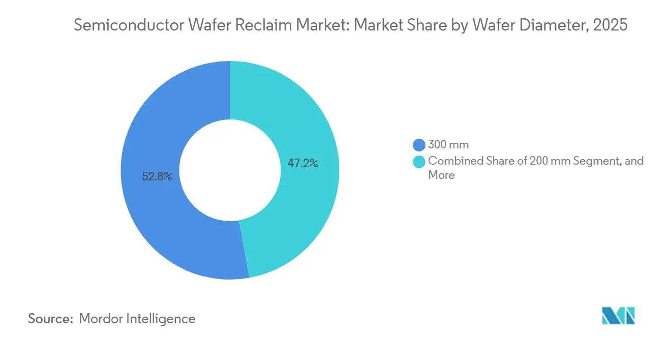
- By wafer diameter, the 300 mm segment led with 52.84% revenue share in 2025, while 200 mm wafers are projected to expand at a 7.28% CAGR through 2031.
- By wafer type, test and monitor wafers commanded 44.98% of the 2025 total, whereas silicon-on-insulator wafers are forecast to grow at a 7.16% CAGR to 2031.
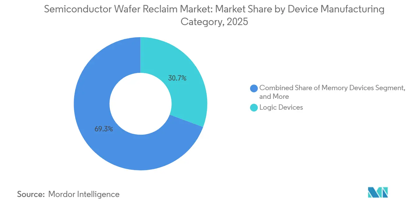
- By device manufacturing category, logic devices held 30.68% of the semiconductor wafer reclaim market share in 2025, while analog and power devices are advancing at a 7.53% CAGR over 2026-2031.
- By geography, Asia-Pacific accounted for 63.79% of 2025 revenue and is expanding at a 6.92% CAGR, maintaining both the largest and fastest-growing regional position.
Note: Market size and forecast figures in this report are generated using Mordor Intelligence’s proprietary estimation framework, updated with the latest available data and insights as of January 2026.
Global Semiconductor Wafer Reclaim Market Trends and Insights
Drivers Impact Analysis*
| Driver | (~) % Impact on CAGR Forecast | Geographic Relevance | Impact Timeline |
|---|---|---|---|
| Expanding 300 mm fab capacity in Asia-Pacific | +1.8% | Asia-Pacific core, spillover to North America | Medium term (2–4 years) |
| Cost-optimization pressure on test and monitor wafers | +1.5% | Global | Short term (≤ 2 years) |
| Sustainability regulations favoring circular-economy practices | +1.2% | Europe and North America, emerging in Asia-Pacific | Long term (≥ 4 years) |
| AI-enabled yield-imaging tools boosting reclaim yields | +0.9% | Global, early adoption in Asia-Pacific and North America | Medium term (2–4 years) |
| Secondary-market demand from low-Earth-orbit satellites | +0.4% | North America and Europe | Long term (≥ 4 years) |
| Foundry shift to SiC and GaN pilot wafers requiring reclaim | +0.5% | Global, concentrated in Asia-Pacific and North America | Long term (≥ 4 years) |
| Source: Mordor Intelligence | |||
Expanding 300 mm Fab Capacity In Asia-Pacific
Asia-Pacific is set to add the bulk of new 300 mm lines through 2027, lifting baseline demand for reclaimed test wafers that account for 15%-20% of every fab’s monthly starts. New plants in Singapore and Taiwan add more than 2 million wafer starts per month, each of which can be reused five to seven times when reclaimed, driving volume elasticity for the semiconductor wafer reclaim market.[1]United Microelectronics Corporation, “UMC Expands Singapore Fab Capacity,” umc.com Dense regional clustering also trims logistics to sub-48-hour cycles, aligning reclaim supply with just-in-time production schedules. Vendors are therefore co-locating facilities near megafabs, locking in multiyear contracts that stabilize cash flow. As additional capacity ramps, reclaim ceases to be a tactical cost lever and becomes a structural component of fab planning.
Cost-Optimization Pressure On Test And Monitor Wafers
Virgin test wafers now cost USD 120-USD 150 per 300 mm piece, up 18% since 2024, pinching gross margins for logic, memory, and power fabs.[2]Siltronic, “Annual Report 2025: Market Dynamics and Pricing Trends,” siltronic.comApplied Materials, “Advanced CMP and Wafer Cleaning Technologies,” appliedmaterials.com Reclaimed substrates drop the effective cost to USD 25-USD 35 after five to eight cycles, yielding immediate savings. Large foundries have validated that reclaimed monitor wafers meet metrology precision without yield loss. Device makers are also deploying machine-learning models to predict remaining reclaim cycles, ensuring wafers retire only when surface roughness limits approach critical thresholds. The economic case is strongest at mature nodes, but even 5 nm facilities now reclaim wafers for non-device steps such as chamber seasoning.
Sustainability Regulations Favoring Circular-Economy Practices
The European Union Chips Act requires subsidized fabs to source 15% reclaimed silicon by 2028, rising to 25% by 2032, creating a policy-driven demand floor that shields vendors from cyclical swings. Similar language in U.S. sustainability grants attaches funding strings to closed-loop manufacturing, unlocking research subsidies for innovation in reclaim processes. Foundries are responding by co-locating reclaim units with virgin-wafer plants, cutting transport emissions, and satisfying scope-3 reporting obligations. Corporate targets, such as a 30% reduction in virgin silicon per wafer by 2030, turn reclaim into a license-to-operate metric rather than a discretionary option.
AI-Enabled Yield-Imaging Tools Boosting Reclaim Yields
Deep-learning inspection now classifies defects on reclaimed wafers in under 10 minutes versus the 90-minute legacy baseline. Fewer false rejects mean wafers survive additional cycles, pushing overall reclaim yield above 95% for test substrates. Reinforcement-learning algorithms simultaneously tune polishing parameters in real time, controlling slurry flow and pad pressure to wafer-specific conditions. As a result, average reclaim life extends from five to seven cycles for 300 mm wafers, improving cost advantage from 60% to nearly 70% relative to virgin silicon. Vendors with the capital to deploy these analytics create a technology moat, accelerating market-share consolidation.
Restraints Impact Analysis*
| Challenge | (~) % Impact on CAGR Forecast | Geographic Relevance | Impact Timeline |
|---|---|---|---|
| Stringent surface-defect specs for 2 nm node | -1.1% | Global, concentrated in Asia-Pacific and North America | Short term (≤ 2 years) |
| Limited skilled labor for advanced polishing lines | -0.7% | Global, acute in North America and Europe | Medium term (2–4 years) |
| Uncertain scrap-silicon pricing volatility | -0.5% | Global | Short term (≤ 2 years) |
| Cyber-security risks in fab-to-reclaim logistics | -0.3% | Global, heightened in Asia-Pacific | Medium term (2–4 |
| Source: Mordor Intelligence | |||
Stringent Surface-Defect Specs For 2 nm Node
Gate-all-around transistors at 2 nm demand surface-defect densities below 0.1 defects per cm², a level reclaim processes struggle to guarantee after multiple polish cycles. The need for atomic-layer cleansing steps adds USD 15-USD 20 per wafer, eroding savings and confining reclaimed wafers to non-critical steps in advanced-node fabs.[3]Applied Materials, “Advanced CMP and Wafer Cleaning Technologies,” appliedmaterials.com Until vendors demonstrate repeatable sub-0.1 nm flatness, leading-edge logic lines will cap reclaim penetration, limiting upside in the most valuable segment of the semiconductor wafer reclaim market.
Limited Skilled Labor For Advanced Polishing Lines
Global shortages of chemical-mechanical polishing technicians delay facility ramps by months, especially in North America and Europe where reshoring outpaces the domestic talent pipeline.[4]Semiconductor Equipment and Materials International, “Global Workforce Survey,” semi.org Training a technician to manage slurry chemistries for silicon, silicon carbide, and gallium nitride lines takes a year or more, and wage premiums exceed 25%. Some operators airlift staff between sites, inflating operating costs and restraining near-term capacity expansion. Workforce development programs are underway, but relief will materialize only after 2027.
*Our forecasts treat driver/restraint impacts as directional, not additive. The impact forecasts reflect baseline growth, mix effects, and variable interactions.
Segment Analysis
By Wafer Diameter: 200 mm Resurgence Driven By Legacy-Node Demand
The 300 mm format accounted for 52.84% of 2025 revenue, anchoring the semiconductor wafer reclaim market size for logic and memory fabs. Yet the 200 mm segment is forecast to rise at 7.28% during 2026-2031, outpacing all other diameters. Automotive and industrial players continue to favor mature nodes for power-management ICs and micro-electromechanical systems, applications that map efficiently onto 200 mm tooling. New silicon-carbide pilot lines at this diameter further widen the addressable base. Reclaim vendors retrofit legacy polishers with endpoint-detection sensors, delivering sub-nanometer control while preserving fully depreciated equipment, which lifts margins without heavy capital outlays. As electrification accelerates, 200 mm reclaim volume will narrow the revenue gap with 300 mm lines even though the latter retains absolute leadership.
Demand for 150 mm reclaim persists in niche aerospace and radiation-hardened circuits, aided by satellite constellations that prefer smaller diameters for cost control on specialized die. Compound-semiconductor substrates often debut at 150 mm before scaling, giving vendors an entry path into future wide-bandgap demand. Collectively, the diameter mix underscores how the semiconductor wafer reclaim market shifts with end-application economics, not just Moore’s Law progression. Vendors diversified across 150 mm through 300 mm lines hedge exposure to any single technology cycle and capture step-wise growth as each diameter finds renewed relevance.


By Wafer Type: SOI Complexity Commands Premium Pricing
Test and monitor wafers dominated 44.98% of 2025 sales, benefiting from predictable demand tied to statistical process control. Rapid 48-hour turnaround and yields above 95% make this category the volume backbone of the semiconductor wafer reclaim market. Conversely, silicon-on-insulator substrates are projected to grow at 7.16% over 2026-2031. The buried-oxide layer complicates polish chemistry, lowering reclaim yields to the 70%-75% range and justifying 40% price premiums. Radio-frequency front-end modules for 5G and automotive radar amplify volume, while Smart Cut donor-wafer reuse models reduce overall substrate cost by 30%, enticing both wafer suppliers and reclaimers into joint ventures.
Prime-wafer reclaim remains limited to R&D environments, where process-integrity stakes are lower and cost sensitivity higher. Epitaxial wafers, used widely in power semiconductors, strike a middle ground with stable mid-single-digit growth and moderate complexity. Profit pools therefore bifurcate: high-volume, low-margin test wafers on one end and lower-volume, high-margin silicon-on-insulator on the other. Firms that master both process extremes insulate themselves from demand swings and capture outsized share of the semiconductor wafer reclaim industry’s profit.
By Device Manufacturing Category: Power Electronics Accelerate Growth
Logic fabs consumed 30.68% of 2025 reclaimed-wafer volume, reflecting heavy use of test wafers during advanced-node yield ramps. Growth is tapering as 2 nm defect specs squeeze reclaim into auxiliary roles, yet the base remains sizable. Analog and power devices are forecast to climb 7.53% through 2031, the fastest across categories. Electrified vehicles, high-efficiency data center power supplies, and grid-edge converters all rely on silicon carbide MOSFETs and insulated-gate bipolar transistors fabricated on reclaimed 200 mm wafers. Stable pricing for these devices gives fabs room to pay premiums for specialized reclaim that prevents metallic cross-contamination.
Memory demand follows predictable cycles of capacity utilization; consolidated producers often lock in long-term contracts with mixed virgin-and-reclaim quotas, producing steady, if unspectacular, growth. Specialty devices, micro-electromechanical systems, sensors, and high-performance RF operate on legacy nodes and small diameters yet command attractive pricing. Vendors that can tailor reclaim chemistries to these diverse material stacks can harvest incremental revenue streams while reinforcing customer stickiness, fortifying their position in the semiconductor wafer reclaim market.
Geography Analysis
Asia-Pacific generated 63.79% of 2025 revenue and grows at 6.92% through 2031, powered by Taiwan, South Korea, China, and Singapore, which together host more than two-thirds of global 300 mm capacity. Co-location strategies shrink wafer-transit time to less than two days, lowering work-in-process inventory for fabs and cementing reclaim as an operational staple. China’s dual-circulation policy further accelerates domestic reclaim capacity, treating local suppliers as a buffer against geopolitical shocks and export controls.
North America captured about 18% of 2025 turnover, but CHIPS Act subsidies are now spawning greenfield fabs from Arizona to Texas. New plants integrate reclaim bays at inception, reflecting circular-economy design principles embedded in funding guidelines. Skilled-labor shortages remain a drag, yet community-college certificate programs are beginning to close the gap, suggesting a medium-term uplift in regional capacity additions and cementing demand for the semiconductor wafer reclaim market in the United States.
Europe held roughly 12% of revenue in 2025, with the EU Chips Act mandating reclaimed-silicon quotas that underpin vendor order books. Co-located operations in Italy and Austria combine virgin and reclaim under one roof, trimming logistics emissions and satisfying regulators. Rest of World countries account for the balance, with Israel’s mature microelectronics cluster and nascent Middle East fab proposals likely to seed incremental demand post-2028. Geography dynamics therefore track fab investments rather than end-market consumption, concentrating growth where capital flows into new wafer starts.

Competitive Landscape
The top five players control an estimated 55%-60% of global revenue, keeping the semiconductor wafer reclaim market moderately concentrated. RS Technologies and Pure Wafer emphasize high-volume test-wafer throughput with 48-hour cycles, leveraging proprietary defect-mapping algorithms to push yields above 95%. Optim Wafer Services positions at the premium end, reclaiming silicon-on-insulator and epitaxial substrates at superior margins. Vertically integrated suppliers such as GlobalWafers and Siltronic bundle reclaim with virgin-wafer sales, spreading metrology and logistics overhead across both businesses for cost leverage.
Technology leadership is the decisive differentiator. AI-assisted inspection and predictive lifetime models allow early adopters to extend reclaim cycles, drive down the effective cost per use, and win share. Equipment suppliers are eyeing the segment through in-situ reclaim modules that could let fabs internalize part of the flow, pressuring stand-alone vendors. Cybersecurity mandates from the National Institute of Standards and Technology add compliance overhead, favoring scale operators able to fund encrypted tracking systems. These forces foreshadow gradual consolidation to a tighter set of global players before 2030, with niche specialists surviving in high-complexity domains such as compound-semiconductor reclaim.
Recent deal activity underscores the strategic premium on capacity and geographic reach. Wafer World’s January 2026 purchase of Micro Reclaim Technologies expands 200 mm capability in North America and deepens exposure to fast-growing automotive power applications. GlobalWafers is investing USD 4 billion in a Phase 2 Texas build-out that co-locates reclaim alongside virgin-wafer output, signaling a push toward one-stop silicon supply for CHIPS Act fabs. RS Technologies’ Taiwan expansion targets compound-semiconductor reclaim, a move that positions the firm to capture silicon-carbide pilot volumes as electrification accelerates. Venture investment is also entering the field, with AI-software startups partnering to license defect-classification models that small and midsize reclaimers cannot afford to build in-house. Together, these initiatives indicate that capital, analytics, and regional co-location will define competitive advantage over the next five years.
Semiconductor Wafer Reclaim Industry Leaders
RS Technologies Co., Ltd.
Pure Wafer, Inc.
GlobalWafers Co., Ltd.
Optim Wafer Services Ltd.
Silicon Valley Microelectronics, Inc.
- *Disclaimer: Major Players sorted in no particular order

Recent Industry Developments
- January 2026: GlobalWafers began design work for a USD 4 billion Phase 2 expansion of its Sherman, Texas plant, adding 300 mm capacity and integrated reclaim to cut lead times to 48 hours for North-American fabs.
- January 2026: Wafer World acquired Micro Reclaim Technologies in Phoenix, adding 50,000 wafer-per-month 200 mm capacity and deepening reach into automotive and power-semiconductor segments.
- October 2025: GlobalWafers opened a Novara, Italy wafer plant that co-locates virgin and reclaim operations, targeting 15% reclaimed-silicon content by 2028 to satisfy EU circularity rules.
- September 2025: RS Technologies announced a Taiwan expansion aimed at 300,000 wafers per month by 2030, equipped with AI defect-inspection to achieve sub-0.1 nm surface control.


Global Semiconductor Wafer Reclaim Market Report Scope
The Semiconductor Wafer Reclaim Market Report is Segmented by Wafer Diameter (150 mm, 200 mm, 300 mm), Wafer Type (Test and Monitor, Prime, Epitaxial, SOI), Device Manufacturing Category (Memory, Logic, Analog and Power, Specialty, R&D), and Geography (North America, Europe, Asia-Pacific, Rest of the World). The Market Forecasts are Provided in Terms of Value (USD).
| 150 mm |
| 200 mm |
| 300 mm |
| Test and Monitor Wafer Reclaim |
| Prime Wafer Reclaim |
| Epitaxial Wafer Reclaim |
| SOI Wafer Reclaim |
| Memory Devices |
| Logic Devices |
| Analog and Power Devices |
| Specialty Devices (MEMS, Sensors, RF) |
| R&D Facilities |
| North America |
| Europe |
| Asia-Pacific |
| Rest of the World |
| By Wafer Diameter | 150 mm |
| 200 mm | |
| 300 mm | |
| By Wafer Type | Test and Monitor Wafer Reclaim |
| Prime Wafer Reclaim | |
| Epitaxial Wafer Reclaim | |
| SOI Wafer Reclaim | |
| By Device Manufacturing Category | Memory Devices |
| Logic Devices | |
| Analog and Power Devices | |
| Specialty Devices (MEMS, Sensors, RF) | |
| R&D Facilities | |
| By Geography | North America |
| Europe | |
| Asia-Pacific | |
| Rest of the World |


Key Questions Answered in the Report
How large will the semiconductor wafer reclaim market be by 2031?
It is projected to reach USD 1.05 billion by 2031 at a 6.4% CAGR from 2026.
Which wafer diameter is growing the fastest?
Reclaimed 200 mm wafers are forecast to expand at a 7.28% CAGR between 2026 and 2031.
Why is Asia-Pacific dominant in reclaimed wafers?
The region houses more than two-thirds of global 300 mm fab capacity, enabling short logistics loops and high test-wafer volumes.
What drives demand in analog and power devices?
Vehicle electrification and grid-edge equipment lift consumption of silicon-carbide and insulated-gate bipolar transistors that rely on reclaimed substrates.
How do AI inspection tools benefit reclaim vendors?
Deep-learning models cut inspection times from 90 minutes to under 10 minutes, extend reclaim cycles, and raise yields above 95%.
What is the main regulatory tailwind for reclaim in Europe?
The EU Chips Act mandates that subsidized fabs source at least 15% reclaimed silicon by 2028, rising to 25% by 2032.
Page last updated on:


