Printed Circuit Board Inspection And Testing Market Size and Share
Market Overview
| Study Period | 2020 - 2031 |
|---|---|
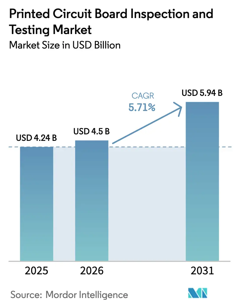
| Market Size (2026) | USD 4.5 Billion |
| Market Size (2031) | USD 5.94 Billion |
| Growth Rate (2026 - 2031) | 5.71% CAGR |
| Fastest Growing Market | Asia Pacific |
| Largest Market | Asia Pacific |
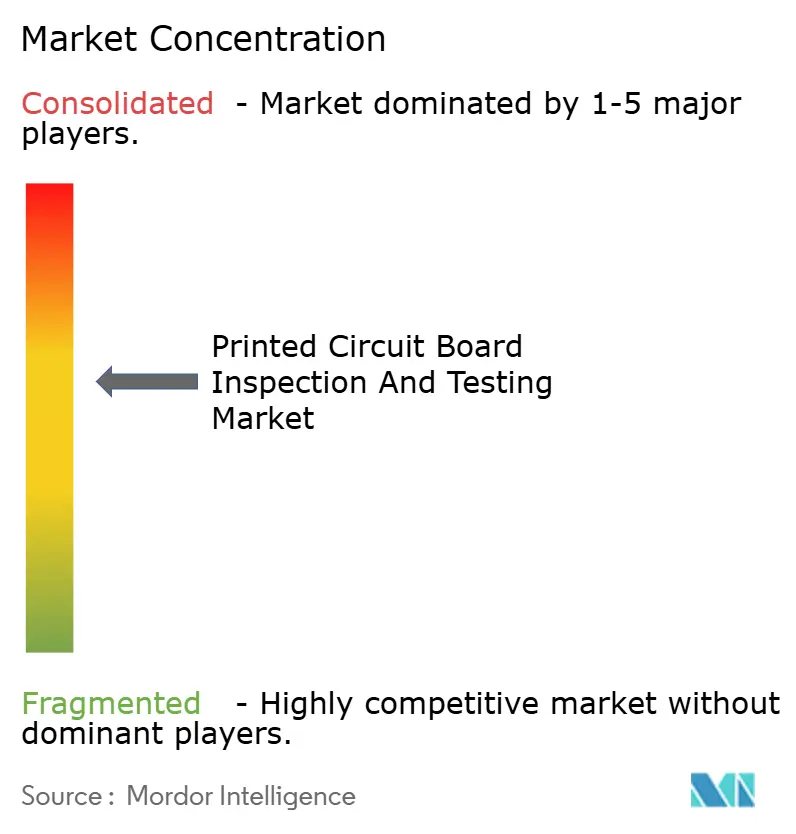
| Market Concentration | Medium |
Major Players *Disclaimer: Major Players sorted in no particular order Image © Mordor Intelligence. Reuse requires attribution under CC BY 4.0. | |
Printed Circuit Board Inspection And Testing Market Analysis by Mordor Intelligence
The Printed Circuit Board inspection and testing market size reached USD 4.5 billion in 2026 and is projected to advance to USD 5.94 billion by 2031, delivering a 5.71% CAGR during the 2026–2031 forecast period, Rising design complexity in automotive electrification, large-scale 5G deployments, and edge-AI devices is tightening defect tolerances, which is pushing manufacturers toward inline automated optical inspection (AOI), X-ray, and integrated test platforms that can sustain yields above 99.5%. Capital expenditure by leading outsourced semiconductor assembly and test (OSAT) providers, spearheaded by ASE Technology’s USD 6 billion 2025 budget, is amplifying demand for high-resolution substrate-inspection tools that detect micro-voids at sub-10-micron levels. Asia-Pacific remains the production hub for printed circuit boards and advanced packaging, and its vendor ecosystem is consolidating around AI-driven 3D AOI platforms that advertise false-positive rates below 1%. Concurrently, macro headwinds- such as shortages of skilled test engineers in Vietnam and India and volatile supply of high-frequency laminates- are prompting interest in inspection-as-a-service and closed-loop smart-factory solutions to protect throughput.
Key Report Takeaways
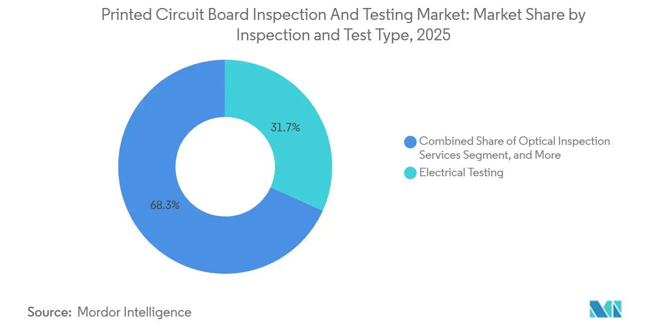
- By inspection and test type, rlectrical testing services commanded 31.73% of the Printed Circuit Board inspection and testing market share in 2025, while X-ray inspection services are projected to grow at a 5.92% CAGR through 2031.
- By manufacturing stage, End-of-line PCBA testing accounted for 47.64% of the Printed Circuit Board inspection and testing market size in 2025, whereas in-process PCBA inspection is set to expand at a 6.13% CAGR during 2026–2031.
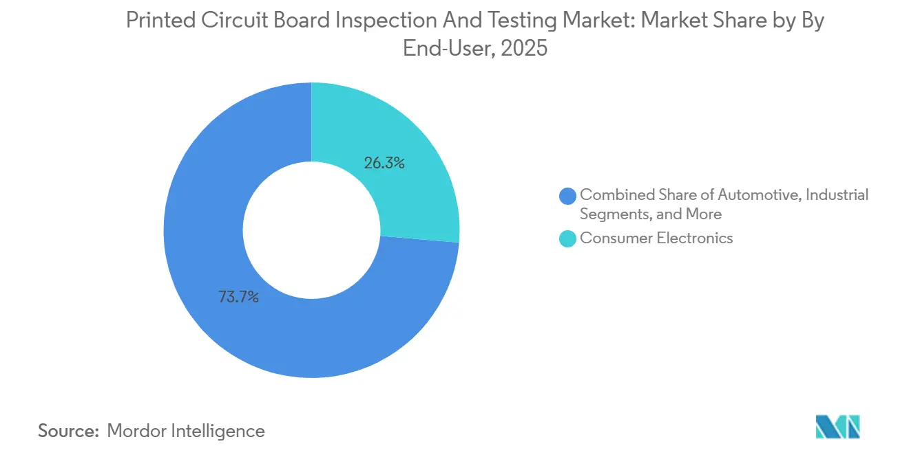
- By end-user, consumer electronics led with 26.33% of demand in 2025, and automotive applications are forecast to post the fastest 6.52% CAGR to 2031.
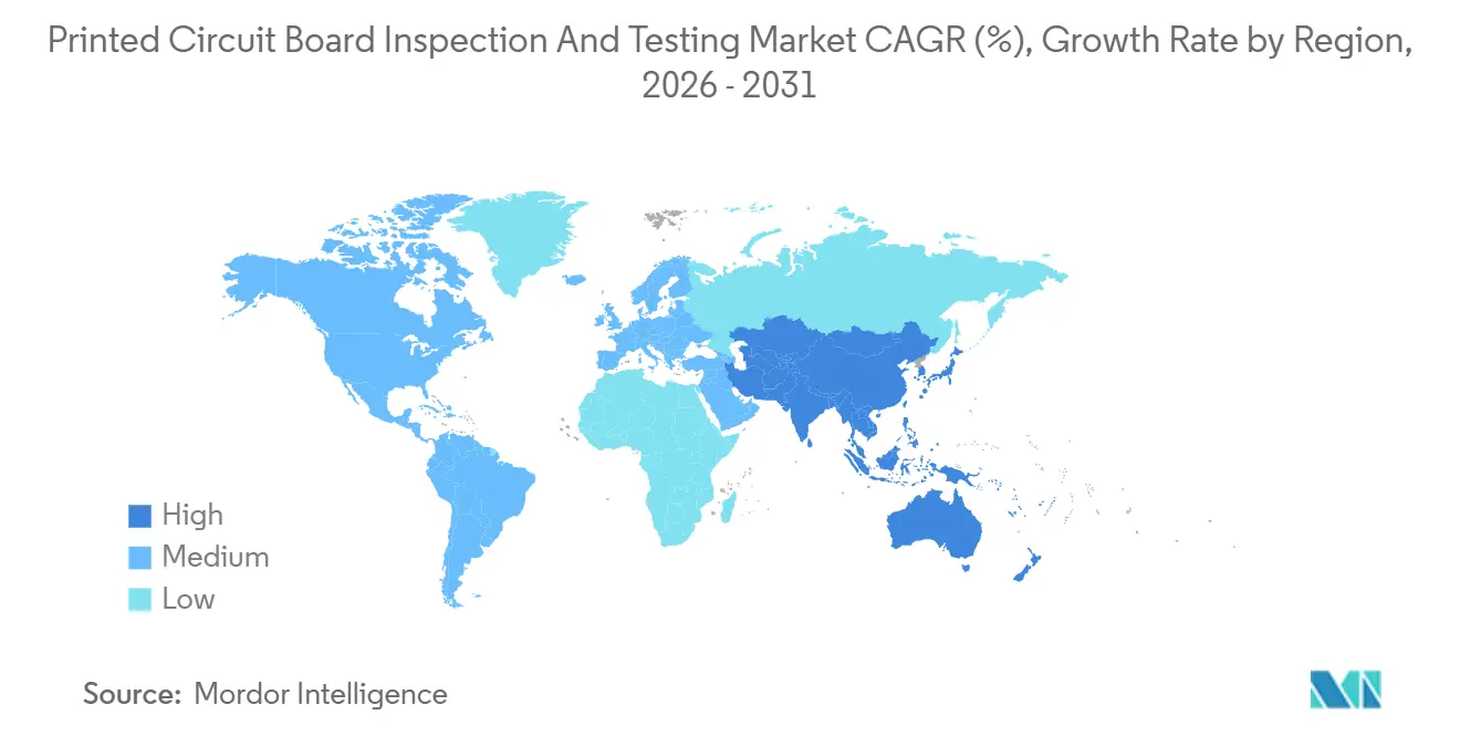
- By region, Asia-Pacific held 70.88% of revenue in 2025, and the region is positioned to record a 7.08% CAGR through 2031.
Note: Market size and forecast figures in this report are generated using Mordor Intelligence’s proprietary estimation framework, updated with the latest available data and insights as of January 2026.
Global Printed Circuit Board Inspection And Testing Market Trends and Insights
Drivers Impact Analysis*
| Driver | (~) % Impact on CAGR Forecast | Geographic Relevance | Impact Timeline |
|---|---|---|---|
| Rapid Miniaturization of Consumer Electronics | +1.2% | Global, with concentration in China, Taiwan, South Korea | Medium term (2-4 years) |
| Increasing Adoption of HDI and FPC Boards in Automotive ADAS | +1.5% | North America, Europe, APAC automotive hubs (Japan, South Korea, China) | Medium term (2-4 years) |
| Transition To 5G-Enabled Telecom Infrastructure | +1.0% | Global, led by China, United States, Europe | Short term (≤ 2 years) |
| Growing Demand for Zero-Defect Manufacturing in IC Substrates | +1.3% | APAC core (Taiwan, China, South Korea), spillover to Southeast Asia | Long term (≥ 4 years) |
| Edge AI Quality-Control Mandates in Smart Factories | +0.8% | Global, early adoption in Germany, Japan, United States | Medium term (2-4 years) |
| Expansion of Semiconductor Back-End OSAT Capacity in Asia-Pacific | +1.4% | Taiwan, China, South Korea, Southeast Asia (Malaysia, Vietnam) | Long term (≥ 4 years) |
| Source: Mordor Intelligence | |||
Increasing Adoption of HDI and FPC Boards in Automotive ADAS
Automotive radar, camera, and lidar modules now mount on multilayer HDI and flexible boards that employ microvias as small as 75 micrometers, making a single open via a potential recall trigger costing millions. Tier-one suppliers must satisfy IPC-A-610 Class 3 zero-defect criteria, so they are installing 100% inline AOI and X-ray stations rather than relying on sample inspection.[1]IPC, “IPC-9716 Process Control Standard for Automated Optical Inspection,” ipc.org Electric-vehicle battery-management systems add more PCBs per car and run across −40 °C to 125 °C thermal cycles, where only 3D X-ray can expose voids before potting. The shift triples board content per vehicle while keeping build volumes lower than in phones, driving demand for flying-probe testers that avoid USD 20,000-50,000 ICT fixtures. Together, these factors lift AOI and AXI penetration, raising the Printed Circuit Board inspection and testing market’s automotive revenue share through 2031.
Expansion of Semiconductor Back-End OSAT Capacity in Asia-Pacific
ASE Technology, King Yuan Electronics, and other OSAT leaders increased 2025 capital outlays beyond USD 7 billion, dedicating large portions to AOI and AXI tools capable of analyzing substrates at sub-10-micron levels. New CoWoS and fan-out lines push defect budgets away from silicon die and onto organic build-up layers with more than 20 stacks, requiring multiple inspection passes per layer. As these fabs ramp, equipment vendors report order backlogs of 9 months, securing a multiyear runway for the Printed Circuit Board inspection and testing market in substrate applications. Emerging Southeast-Asian sites in Malaysia and Vietnam follow Taiwan’s process recipes, widening regional demand diversity. Long payback cycles encourage inspection-as-a-service pilots that bundle metrology hardware, software, and analytics under outcome-based contracts.
Growing Demand for Zero-Defect Manufacturing in IC Substrates
Advanced packages, such as the chip-on-wafer-on-substrate route, copper traces at 10 micrometers, which magnifies the cost of every latent open or void. OSATs now link high-speed AOI, AXI, and surface-metrology data to statistical process-control dashboards that flag excursions within minutes instead of hours. This closed-loop approach reduced scrap rates by up to 40% on pilot lots of AI accelerators shipped in 2025, according to vendor field reports. The resulting savings justify premium tool sets that exceed USD 1 million each, supporting above-market growth for high-resolution inspection platforms. Consequently, substrate fabs are the fastest-expanding spenders inside the broader Printed Circuit Board inspection and testing market.
Rapid Miniaturization of Consumer Electronics
Smartphone mainboards now carry component pitches of 0.3 millimeter or less, overwhelming legacy 2D AOI optics. ViTrox’s dual-sided V510Ai platform, introduced in August 2025, inspects both board faces simultaneously, reducing cycle time by 40% and proving essential for high-volume handset lines. Rigid-flex wearables feature severe bend radii below 1 millimeter, so multispectral imaging can differentiate solder from polyimide glare without increasing false-call rates. The December 2024 IPC-9716 standard demands traceable false-positive metrics, steering buyers toward systems with built-in audit trails. Collectively, these shifts boost premium AOI adoption, sustaining growth in the Printed Circuit Board inspection and testing market despite rapid price erosion in consumer devices.
Restraints Impact Analysis*
| Restraint | (~) % Impact on CAGR Forecast | Geographic Relevance | Impact Timeline |
|---|---|---|---|
| Capital-Intensive Nature of Inline AOI And AXI Systems | -0.9% | Global, acute in emerging markets (India, Vietnam, Mexico) | Short term (≤ 2 years) |
| Shortage Of Skilled Test Engineers in Emerging Regions | -0.6% | Southeast Asia, India, Mexico, Eastern Europe | Medium term (2-4 years) |
| Fragmented Standards Across Regions and Industries | -0.4% | Global, particularly North America and Europe vs. Asia-Pacific | Long term (≥ 4 years) |
| Volatility in Substrate Material Supply Chain | -0.5% | Global, with acute impact on high-frequency PCB manufacturers | Short term (≤ 2 years) |
| Source: Mordor Intelligence | |||
Capital-Intensive Nature of Inline AOI and AXI Systems
Entry-level 2D AOI platforms start near USD 150,000, 3D AOI exceeds USD 400,000, and computed-tomography AXI surpasses USD 1 million, figures that strain the balance sheets of small and mid-size assemblers. High-mix lines rarely amortize such investments within 3 years, delaying adoption in fast-growing regions like Vietnam and India, where contract manufacturers are chasing smartphone and automotive transfers from China. Leasing and pay-per-use models are emerging, yet they shift utilization risk to equipment vendors and require accurate volume forecasts that many local firms cannot supply. As a result, smaller plants remain on flying-probe testers or outsource inspection, slowing overall penetration of advanced systems in the market.
Shortage of Skilled Test Engineers in Emerging Regions
Vietnam attracted USD 2.5 billion in electronics investment during 2025 but faced a gap of roughly 15,000 trained test engineers, forcing companies to rotate specialists from Taiwan at premium wages. India’s electronics workforce expanded by 18% in 2025, yet vocational programs lag industry needs by up to 2 years, hampering automotive and medical device ramps that mandate IPC-A-610 Class 3 compliance.[2]IPC, “IPC-A-610 Acceptability of Electronic Assemblies,” ipc.org AOI and AXI tools embed AI classifiers to reduce manual tuning, but borderline defects still demand human judgment, limiting fully lights-out operations. This talent bottleneck tempers the momentum of installation for sophisticated platforms in the Printed Circuit Board inspection and testing market in the medium term.
*Our forecasts treat driver/restraint impacts as directional, not additive. The impact forecasts reflect baseline growth, mix effects, and variable interactions.
Segment Analysis
By Inspection and Test Type: X-Ray Gains as Subsurface Defects Multiply
Electrical testing services captured 31.73% of the Printed Circuit Board inspection and testing market share in 2025, underscoring their entrenched role as the final electrical integrity gate before functional test. Within the same year, X-ray platforms accounted for a smaller slice of the Printed Circuit Board inspection and testing market size but are projected to post the fastest 5.92% CAGR through 2031, propelled by ball-grid-array, quad-flat-no-lead, and heterogeneous-integration packages that hide defects beneath solder joints. Automotive inverters, 5G radio modules, and AI accelerator substrates mandate volumetric void analysis, prompting tier-one suppliers to specify 3D computed-tomography AXI as a qualification requirement for new lines. Flying-probe electrical testers remain favored for prototypes and high-mix production because they avoid the USD 20,000-50,000 fixture cost of in-circuit test, but their cycle times limit use in smartphone factories that build tens of thousands of boards per hour. Optical inspection retains dominance for surface anomalies such as tombstoning and bridging, with Saki’s integrated SPI-AOI platform trimming floor space by 30% to free up space for additional X-ray stations.[3]Saki Corporation, “3Si/3Di-EX Integrated SPI and AOI,” sakicorp.com Vendors now bundle defect-classification AI across optical and X-ray modalities to consolidate data dashboards, reducing engineering headcount per line.
X-ray’s rapid uptake is already shifting quoting practices. Contract manufacturers bid turnkey projects that include AXI as a baseline capability rather than a chargeable option, a change that compresses margins for plants that still lack the technology. Equipment suppliers answer by offering usage-based subscriptions that mix hardware, analytics, and service into one monthly fee, lowering entry barriers for Southeast-Asian factories chasing smartphone subassembly transfers from China. In parallel, regulatory bodies such as the FDA are tightening counterfeit-component screening rules for implantable electronics, which is set to widen the customer base beyond traditional computing and telecom verticals. As a result, the inspection-type landscape will likely show a smaller electrical-test share and a materially larger X-ray slice when the Printed Circuit Board inspection and testing market share metrics are recalculated for 2031.


By Manufacturing Stage: In-Process Inspection Closes the Feedback Loop
End-of-line PCBA testing accounted for 47.64% of the Printed Circuit Board inspection and testing market size in 2025, reflecting decades-old quality philosophies that relied on a final gate to stop defective boards. Meanwhile, in-process PCBA inspection is forecast to expand at a 6.13% CAGR through 2031, the fastest among stage categories, as Industry 4.0 programs link AOI, AXI, and solder-paste inspection to upstream machines within 200 milliseconds. Real-time feedback trims scrap and rework by up to 40% on smartphones and automotive radar modules, quickly offsetting the capital premium of inline AOI lines. EMS providers now combine inner-layer AOI with drilling-stage X-ray to eliminate latent defects that optical cameras cannot visualize. Boundary-scan instruments added to end-of-line cells allow access to high-speed nets where physical pads no longer exist, restoring coverage on densely routed server boards.
As more plants adopt closed-loop control, in-process systems will account for a larger slice of the Printed Circuit Board inspection and testing market share by 2031, while standalone end-of-line testers plateau. The migration is most pronounced in high-volume handset lines across China and Vietnam, yet automotive and medical assemblers in North America and Europe are following because zero-defect mandates now penalize latent field failures. Collectively, these advances reinforce the thesis that dynamic, data-rich inspection stages will be the prime growth engine inside the Printed Circuit Board inspection and testing industry for the remainder of the decade.
By End-User: Automotive Electrification Rewrites Inspection Protocols
Consumer electronics represented 26.33% of PCB inspection and testing market demand in 2025, preserving its lead on shipment volume despite severe price pressure. Automotive, however, is projected to register the fastest 6.52% CAGR to 2031, driven by electric-vehicle powertrains that triple board count per car and impose IPC-A-610 Class 3 zero-defect thresholds on every solder joint. Battery-management system boards running at 800 V currents rely on void-free thermal vias, so tier-one suppliers now order 100% AXI coverage and reject lots with more than 25% voiding per joint. ADAS controllers integrate radar, lidar, and camera processing on HDI boards with microvias as small as 75 micrometers, where a single open can trigger million-dollar recalls, further increasing inspection intensity. Aerospace and defense builders pair burn-in stress tests with AOI to meet AS9100 guidelines, while data-center server manufacturers extend inspection downstream to organic substrates as chiplet architectures spread.
Over the forecast term, automotive’s growing share will slightly dilute consumer electronics’ dominance, but both segments will together preserve more than half of the Printed Circuit Board inspection and testing market size. Auto OEMs are adding supplier scorecards that reward sub-1% escape rates, so inspection vendors embed machine-learning classifiers that shrink false positives without letting defects slip. Consequently, the PCB inspection and testing market share gains will favor vendors capable of spanning optical, X-ray, and electrical modalities under unified analytics dashboards that comply with each sector’s audit trail requirements.
Geography Analysis
Asia-Pacific dominated the Printed Circuit Board inspection and testing market share with 70.88% of global revenue in 2025 and is forecast to compound at a 7.08% CAGR through 2031, reflecting its dense cluster of PCB fabs and OSAT lines in Taiwan, China, and South Korea. Taiwan alone is expanding CoWoS capacity from 80,000 wafers per month to as high as 130,000 by late 2027, which is escalating orders for sub-10-micron substrate-inspection tools. China’s domestic AOI equipment spending totaled CNY 22.781 billion (USD 3.19 billion) in 2024 and has been rising at an 11.05% annual clip as state incentives fuel semiconductor self-sufficiency.[4]China Electronics Standardization Institute, “China AOI Equipment Market,” cesi.cn Japan and South Korea are directing new capital toward automotive-electronics inspection to meet IPC Class 3 standards for battery-management and traction-inverter boards. Southeast Asia, led by Vietnam and Malaysia, is attracting smartphone and server assembly migration yet faces an 18-to-24-month training gap for skilled test engineers, a shortfall that is slowing local uptake of inline AOI cells.
North America holds a mid-single-digit share of the Printed Circuit Board inspection and testing market, but the aerospace, defense, and medical verticals are driving above-average tool revenue per line, as FDA 21 CFR 820 and AS9100 audits require documented AOI and AXI false-escape metrics. U.S. advanced-packaging pilots run by Intel, Amkor, and SkyWater are specifying substrate-inspection accuracy below 1 micron, a threshold that favors premium computed-tomography X-ray systems. Europe is channeling automotive-electronics funding into German, French, and Italian plants as the European Chips Act steers incentives toward domestic OSAT capacity, which will necessitate high-resolution inspection spend through 2028
The rest of world cluster- South America, the Middle East, and Africa- accounts for a low-single-digit portion of global revenue and remains centered on lower-complexity consumer electronics. Mexico is emerging as a nearshoring node for North American automotive boards, yet many contract manufacturers still rely on flying-probe testers due to capital constraints. Gulf-region investments in industrial IoT and solar-inverter plants could stimulate demand for high-power board inspection, but most projects remain in feasibility stages. Consequently, mature vendors are pursuing inspection-as-a-service pilots that bundle hardware, analytics, and remote expertise to seed adoption in these nascent markets.

Competitive Landscape
The top five suppliers- Koh Young Technology, Omron Corporation, ViTrox Corporation, Keysight Technologies, and KLA Corporation through its Orbotech unit- collectively generated a considerable amount of 2025 revenue, confirming a moderately concentrated structure that still leaves ample share for regional specialists. Each of these leaders is racing to embed deep-learning algorithms that suppress false positives below 1% and export defect data to line-control software in sub-second intervals, features now mandatory for smartphone and automotive customers. Koh Young’s Zenith 2 platform, showcased at SMTA International in October 2025, claims closed-loop feedback to printers and placement machines within 200 milliseconds, cutting scrap rates by up to 40% in pilot runs for high-density handset boards.
Regional challengers such as Shenzhen JT Automation and Unicomp Technology erode list prices by 20-30% inside China, capitalizing on provincial subsidies that favor domestic content. These firms have grown quickly in consumer-electronics assembly but face hurdles in medical and aerospace projects, where OEMs demand audited compliance with IPC-9716 and IPC-A-610 Class 3 requirements. Wabtec’s USD 1.78 billion purchase of Evident’s Inspection Technologies division in July 2025 signals broader industrial-equipment entrants are eyeing the electronics test space, especially rail and energy clients that require non-destructive evaluation across PCBs, castings, and welds.
Service-based business models are gaining momentum as small and medium-size enterprises struggle to fund USD 400,000-plus 3D AOI or USD 1 million CT-AXI machines; ViTrox and Omron now pilot subscription bundles that charge per inspected board rather than hardware sale. Software is also emerging as a moat, Koh Young, KLA, and Omron expose application-programming interfaces that pull defect images into cloud analytics engines, enabling predictive stencil replacement or reflow-profile tuning with minimal human supervision. Start-ups focused on AI-assisted root-cause analysis- linking inspection escapes to pick-and-place nozzle wear or solder-paste viscosity drift- are courting tier-one EMS plants, and larger vendors respond with minority investments or exclusive licenses.
Printed Circuit Board Inspection And Testing Industry Leaders
Koh Young Technology Inc.
Omron Corporation
KLA Corporation
ViTrox Corporation Berhad
Test Research Inc.
- *Disclaimer: Major Players sorted in no particular order

Recent Industry Developments
- October 2025: Koh Young Technology showcased the Zenith 2 automated optical inspection platform at SMTA International, highlighting deep-learning defect classification with false-positive rates below 1% and 200 millisecond feedback to upstream process equipment.
- August 2025: ViTrox Corporation began shipping the V510Ai dual-sided automated optical inspection system, which scans both board faces in one pass and reduces inspection cycle time by 40%.
- July 2025: Wabtec Corporation completed its USD 1.78 billion acquisition of Evident’s Inspection Technologies division, integrating automated optical, X-ray, and ultrasonic testing portfolios under one industrial-inspection platform.
- June 2025: Axxon and Mycronic jointly launched the Modus CCAOI conformal-coating automated optical inspection system, using multispectral imaging to verify coating thickness and uniformity on automotive and aerospace boards.
- April 2025: Saki Corporation released the 3Si and 3Di-EX series that combine solder-paste inspection and post-reflow AOI in a single enclosure, trimming factory floor space by 30%.


Global Printed Circuit Board Inspection And Testing Market Report Scope
The Printed Circuit Board Inspection and Testing Market encompasses the processes, services, and technologies used to inspect and test printed circuit boards (PCBs) to ensure their quality, functionality, and compliance with industry standards. This includes various inspection and testing methods applied at different manufacturing stages, catering to diverse end-user industries.
The Printed Circuit Board Inspection and Testing Market Report is Segmented by Inspection and Test Type (Optical Inspection Services, X-ray Inspection Services, Electrical Testing Services, Functional Testing Services, and Burn-in/Stress Screening), Manufacturing Stage (Bare PCB Inspection, In-Process PCBA Inspection, and End-of-Line PCBA Testing), End-User (Consumer Electronics, Automotive, Industrial, Medical, Communication and Networking, Aerospace and Defense, Computing, and Other End-users), and Geography (North America, Europe, Asia-Pacific, and Rest of World). The Market Forecasts are Provided in Terms of Value (USD).
| Optical Inspection Services |
| X-ray Inspection Services |
| Electrical Testing Services |
| Functional Testing Services |
| Burn-in / Stress Screening |
| Bare PCB Inspection |
| In-Process PCBA Inspection |
| End-of-Line PCBA Testing |
| Consumer Electronics |
| Automotive |
| Industrial |
| Medical |
| Communication and Networking |
| Aerospace and Defense |
| Computing |
| Other End-users |
| North America | United States |
| Rest of North America | |
| Europe | Germany |
| United Kingdom | |
| Netherlands | |
| Rest of Europe | |
| Asia-Pacific | China |
| Taiwan | |
| Japan | |
| India | |
| South Korea | |
| Southeast Asia | |
| Rest of Asia-Pacific | |
| Rest of World |
| By Inspection and Test Type | Optical Inspection Services | |
| X-ray Inspection Services | ||
| Electrical Testing Services | ||
| Functional Testing Services | ||
| Burn-in / Stress Screening | ||
| By Manufacturing Stage | Bare PCB Inspection | |
| In-Process PCBA Inspection | ||
| End-of-Line PCBA Testing | ||
| By End-User | Consumer Electronics | |
| Automotive | ||
| Industrial | ||
| Medical | ||
| Communication and Networking | ||
| Aerospace and Defense | ||
| Computing | ||
| Other End-users | ||
| By Region | North America | United States |
| Rest of North America | ||
| Europe | Germany | |
| United Kingdom | ||
| Netherlands | ||
| Rest of Europe | ||
| Asia-Pacific | China | |
| Taiwan | ||
| Japan | ||
| India | ||
| South Korea | ||
| Southeast Asia | ||
| Rest of Asia-Pacific | ||
| Rest of World | ||


Key Questions Answered in the Report
What is the projected value of global PCB inspection and testing activities by 2031?
The market is forecast to reach USD 5.94 billion by 2031.
Which inspection modality is growing fastest through 2031?
X-ray inspection services are expected to post the highest 5.92% CAGR because they detect subsurface defects invisible to optical systems.
Why is Asia-Pacific considered the key region for PCB inspection demand?
The region hosts more than 70% of PCB fabrication and OSAT capacity, and its fabs are expanding advanced-packaging lines that require high-resolution inspection.
How are automotive trends influencing inspection requirements?
Electric-vehicle power modules and ADAS boards impose IPC-A-610 Class 3 zero-defect standards, driving 100% AOI and X-ray coverage on every unit.
What barriers slow adoption for small and mid-size manufacturers?
Capital costs exceeding USD 400,000 for 3D AOI and USD 1 million for CT-X-ray systems, along with shortages of skilled test engineers, delay equipment purchases in emerging markets.
Page last updated on:


