Prime Polished Wafer Market Size and Share
Market Overview
| Study Period | 2020 - 2031 |
|---|---|
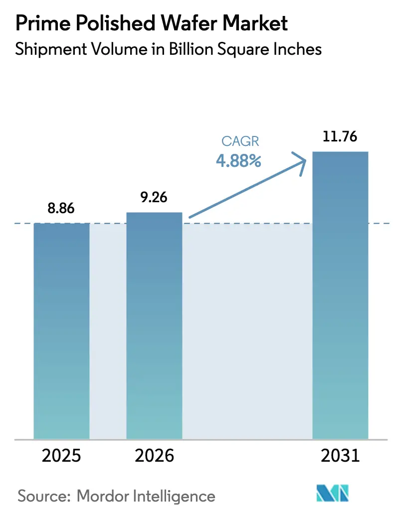
| Market Volume (2026) | 9.26 Billion Square Inches |
| Market Volume (2031) | 11.76 Billion Square Inches |
| Growth Rate (2026 - 2031) | 4.88% CAGR |
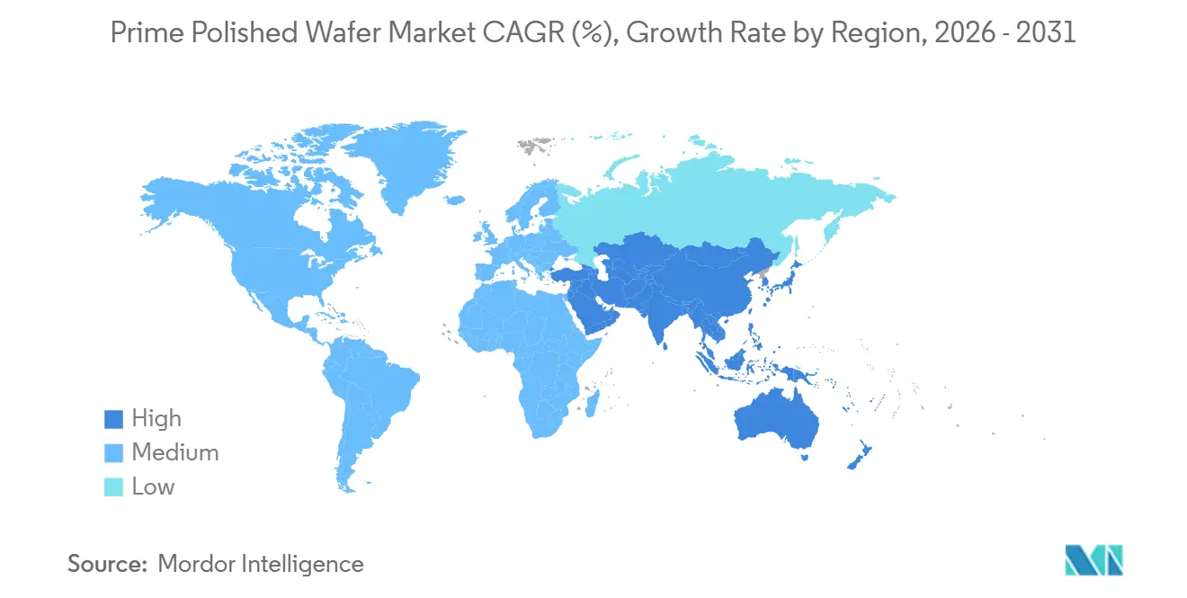
| Fastest Growing Market | Asia Pacific |
| Largest Market | Asia Pacific |
| Market Concentration | High |
Major Players
*Disclaimer: Major Players sorted in no particular order Image © Mordor Intelligence. Reuse requires attribution under CC BY 4.0. |
|
Prime Polished Wafer Market Analysis by Mordor Intelligence
The prime polished wafer market size is projected to be 8.86 billion square inches in 2025, 9.26 billion square inches in 2026, and reach 11.76 billion square inches by 2031, growing at a CAGR of 4.88% from 2026 to 2031. Semiconductor manufacturers are reallocating capital toward advanced logic nodes, automotive electrification, and high-bandwidth memory, all of which consume wafer surface area far more rapidly than traditional consumer-electronics refresh cycles. Foundries’ shift to sub-3 nm process technology, coupled with the ramp-up of through-silicon-via packaging, is concentrating demand in the 300 mm diameter class that already dominates the prime polished wafer market. Asia-Pacific’s contract manufacturing base keeps the region in a leadership position, while the United States and Europe are using incentive packages to on-shore strategic capacity despite the resulting cost penalties. Suppliers remain cautious on new crystal-growth investments because each 300 mm high-purity ingot line ranges from USD 2 million to USD 5 million and can take two years to qualify.
Key Report Takeaways
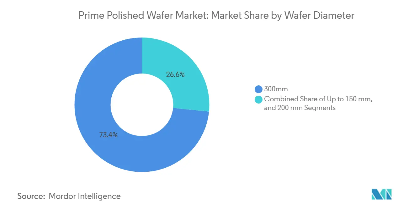
- By wafer diameter, the 300 mm class captured 73.39% of prime polished wafer market share in 2025. The segment is forecast to expand at a 5.55% CAGR through 2031.
- By semiconductor device type, logic held 44.84% of prime polished wafer market size in 2025, while the same segment is advancing at a 4.9% CAGR through 2031.
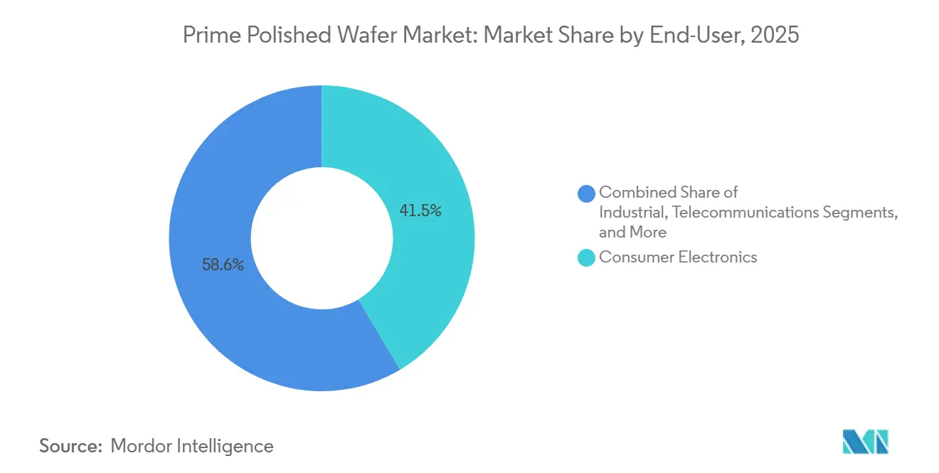
- By end-user, consumer electronics accounted for 41.45% of demand in 2025. Automotive is the fastest-growing end-user, rising at a 5.39% CAGR to 2031.
- By geography, Asia-Pacific dominated with 81.39% share of the silicon wafer market size for memory devices in 2025 and is advancing at a 5.21% CAGR through 2031.
Note: Market size and forecast figures in this report are generated using Mordor Intelligence’s proprietary estimation framework, updated with the latest available data and insights as of January 2026.
Global Prime Polished Wafer Market Trends and Insights
Drivers Impact Analysis*
| Driver | (~) % Impact on CAGR Forecast | Geographic Relevance | Impact Timeline |
|---|---|---|---|
| Rising EV Penetration and Shift Toward 800-V Vehicle Platforms | +1.2% | Global, led by China, Europe, North America | Medium term (2–4 years) |
| Rapid Build-Out of 800-V Charging Infrastructure | +0.9% | Europe and China lead; North America emerging | Medium term (2–4 years) |
| High-Temperature, High-Frequency Performance Advantages Over Si | +0.8% | Global industrial and automotive | Long term (≥ 4 years) |
| Government Incentives for Wide-Band-Gap Fabs | +0.7% | North America, Europe, Japan, China | Short term (≤ 2 years) |
| Emergence of Vertically Integrated SiC Supply Chains in China | +0.5% | China, spillover to Asia-Pacific | Medium term (2–4 years) |
| Novel 200 mm Bulk-Growth Breakthroughs Lowering Defect Density | +0.4% | Japan and United States | Long term (≥ 4 years) |
| Source: Mordor Intelligence | |||
Rising EV Penetration and Shift Toward 800-V Vehicle Platforms
Electric vehicles adopting 800-volt architectures require silicon-carbide traction inverters that consume far larger prime polished wafer volumes per car than silicon devices. Wolfspeed’s commercial 200 mm SiC launch in September 2025 increases chips-per-wafer by roughly 85%, yet supply is still bottlenecked by 7- to 14-day crystal-growth cycles.[1]Wolfspeed, "Add Miles and Years of Performance to Your Next 800-V EV Traction Inverter Platform", wolfspeed.com Multiple major automakers already qualify SiC MOSFETs rated up to 1,200 V, pushing demand firmly upward.
Rapid Build-Out of 800-V Charging Infrastructure
Europe and China are adding thousands of 150- to 350-kW charging stalls that embed SiC modules for rectification and power-factor correction. Each ultra-fast charger needs multiple 200 mm wafers, creating a second-order pull on the prime polished wafer market. Subsidies accelerate installation schedules, compressing suppliers’ ability to add new boule capacity.
High-Temperature, High-Frequency Performance Advantages Over Si
SiC’s 3.26 eV bandgap, 4.9 W cm⁻¹ K⁻¹ thermal conductivity, and electric-field strength 10 times higher than Si allow devices to run > 200 °C junction temperatures and > 100 kHz switching. System-level efficiencies, lower cooling overhead, and reduced passive component counts offset wafer cost premiums of up to 10 times compared with silicon. Industrial drives and renewable inverters are therefore adopting SiC ahead of schedule.
Government Incentives for Wide-Band-Gap Fabs
The United States CHIPS Act (USD 52.7 billion), EU Chips Act (EUR 43 billion – USD 47 billion), Japan’s JPY 2 trillion package (USD 13 billion), and China’s USD 47.5 billion IC Fund Phase III collectively lower capital costs by 20-35% for new wide-band-gap lines.[2]european-chips-act, "USA_Semiconductor_Legislation", european-chips-act.com Wolfspeed, GlobalWafers, and SK Siltron already secured awards, shortening fab payback periods and stimulating near-term capacity announcements.
Restraints Impact Analysis*
| Restraint | (~) % Impact on CAGR Forecast | Geographic Relevance | Impact Timeline |
|---|---|---|---|
| Limited Availability of 200 mm Substrates | -0.6% | Acute in North America and Europe | Short term (≤ 2 years) |
| Packaging-Induced Thermo-Mechanical Stress | -0.4% | Automotive and industrial globally | Medium term (2–4 years) |
| Capital-Intensive Crystal-Growth Equipment | -0.3% | Global | Long term (≥ 4 years) |
| Recycling Challenges for SiC Kerf Waste | -0.2% | Europe and North America | Long term (≥ 4 years) |
| Source: Mordor Intelligence | |||
Limited Availability of 200 mm Substrates
200 mm SiC boules require long growth times and specialized furnaces. Substrate lead times stretch beyond 40 weeks for smaller customers as automotive OEMs lock in multi-year contracts, leaving the rest of the prime polished wafer market scrambling for allocation.
Packaging-Induced Thermo-Mechanical Stress
Mismatched coefficients of thermal expansion between SiC die, substrates, and encapsulants introduce delamination risk in 1,000-cycle automotive stress tests. Silver-sintered die-attach and ceramic bases mitigate failures but add USD 5-USD 15 per device and lengthen qualification cycles, slowing wafer demand ramp-up.
*Our forecasts treat driver/restraint impacts as directional, not additive. The impact forecasts reflect baseline growth, mix effects, and variable interactions.
Segment Analysis
By Wafer Diameter: Advanced Nodes Drive 300 mm Dominance
The 300 mm class accounted for 73.39% of prime polished wafer market share in 2025 and is forecast to grow at a 5.55% CAGR through 2031. TSMC’s USD 56 billion capital plan for 2026, of which 70-80% goes to sub-3 nm logic, underscores the relentless shift toward large-diameter processing. The prime polished wafer market size for this diameter will continue expanding as high-bandwidth memory and AI accelerators require four-to-eight times more wafer area per server than conventional workloads. Intel’s USD 165 billion Arizona “gigafab” cluster and GlobalWafers’ Texas line add regional redundancy, satisfying domestic-content rules while creating new logistic hubs.
The 200 mm segment remains essential for analog, mixed-signal, and power devices, particularly SiC MOSFETs where the economics still favor smaller diameters. Okmetic’s Finnish expansion and Wolfspeed’s 200 mm SiC wafers show the dual-track strategy of suppliers addressing both mainstream silicon and specialty needs. Up-to-150 mm formats are declining, yet they persist in legacy automotive microcontrollers and RF GaAs devices. As crystal-growth breakthroughs reduce defect densities, 200 mm SiC supply could loosen post-2028, but near-term scarcity keeps prices elevated and reinforces multi-sourcing behavior among fabs.


By Semiconductor Device Type: Logic Leads AI-Driven Consumption
Logic devices consumed 44.84% of prime polished wafer market size in 2025, reflecting AI accelerators and disaggregated chiplet architectures that inflate wafer counts per finished package. TSMC indicated that nodes ≤ 5 nm generated 63% of Q4 2025 wafer revenue, evidence of sustained migration toward advanced geometries. High-bandwidth memory, consuming 70% of global through-silicon-via capacity, further tightens substrate supply and drives cross-segment competition.
Memory’s relative share is sliding because wafer capacity is disproportionately captured by logic and specialty devices, even though absolute DRAM and NAND volumes remain large. Discrete power and optoelectronics, while smaller slices of the prime polished wafer market, are expanding rapidly as data-center transceivers migrate to 800 Gb and 1.6 Tb links fabricated on 300 mm photonics platforms. Tower Semiconductor doubled its silicon-photonics revenue in 2025 to USD 228 million, highlighting entrant opportunities for value-added surface treatments and wafer bonding.
By End-User: Automotive Outpaces Consumer Electronics Growth
Consumer electronics held 41.45% of demand in 2025, but extended smartphone replacement cycles are capping incremental wafer growth. In contrast, automotive semiconductor content is heading toward USD 1,000 per electric vehicle by 2030, pulling SiC demand at a 5.39% CAGR through 2031.[3]NITI Aayog, "Automotive Industry Powering India’s participation in Global Value Chains", niti.gov Each 800-V EV integrates four to six SiC MOSFET dies, significantly bolstering wafer intensity.
Industrial and renewable sectors are also embracing wide-band-gap devices to slash energy losses and cooling overhead. Telecommunications upgrades to 5 G and optical backhaul expand RF front-end and photonics consumption. These high-reliability niches value supply continuity, prompting multi-year contracts that stabilize the prime polished wafer market even during consumer downturns.
Geography Analysis
Asia-Pacific shipped 81.39% of global prime polished wafer volumes in 2025 and is set to grow at 5.21% CAGR through 2031. Regional giants such as TSMC, Samsung, and SK Siltron continue expanding deeply integrated clusters that bundle front-end, packaging, and testing. China’s SMIC added 40 k 12-inch-equivalent wafers per month in 2026, achieving 95.7% utilization despite tool export controls. Subsidies under China’s USD 47.5 billion IC Fund Phase III buttress domestic SiC supply chains.
North America is reversing decades of offshoring by tapping USD 39 billion in CHIPS incentives. GlobalWafers’ USD 3.5 billion Texas plant, Intel’s Arizona gigafab, and Wolfspeed’s SiC mega-facility collectively drive a region-wide surge in demand for prime polished wafers. Mexico’s ascending role in assembly and test adds downstream pull.
Europe remains fab-constrained for leading-edge logic yet excels in strategic materials. STMicroelectronics secured EUR 2.9 billion (USD 3.2 billion) to scale SiC in Italy, and discussions continue on a potential TSMC-run Dresden fab that would localize 300 mm automotive capacity. Soitec and Siltronic provide regionally anchored SOI and high-flatness substrates, keeping Europe relevant in the prime polished wafer market value chain. Emerging investments across South America and the Middle East and Africa favor mature-node fabs servicing automotive and industrial customers close to end markets.

Competitive Landscape
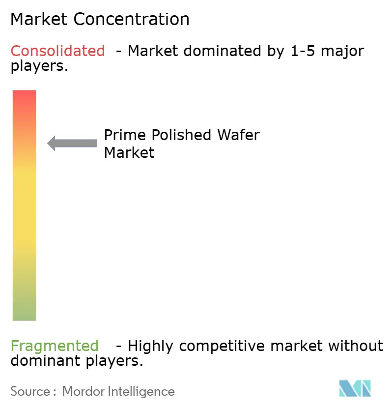
The prime polished wafer market shows moderate concentration; Shin-Etsu and SUMCO supply roughly 50% of worldwide volume, yet customers mitigate dependency through dual-sourcing. Advanced flatness specifications below 0.15 µm for sub-3 nm nodes allow a 10-15% pricing premium for best-in-class suppliers.
Strategic geographic diversification is under way. GlobalWafers’ Texas and SK Siltron’s Michigan SiC sites anchor U.S. supply, while TSMC’s Kumamoto expansion in Japan and possible Dresden joint venture anchor redundancy outside Taiwan. Capacity is increasingly allocated through multi-year contracts underpinned by customer pre-payments, locking more than 70% of Tower Semiconductor’s silicon-photonics output through 2028.
Technical competition is shifting to surface preparation for wafer-to-wafer bonding, TSV, and heterogeneous integration, areas where smaller specialty players can out-innovate scale leaders. Chinese entrants such as SICC and Hangzhou Crystal Silicon capture domestic market share under subsidy-backed expansion, potentially redistributing 200 mm SiC demand away from Japanese and European incumbents after 2028.
Prime Polished Wafer Industry Leaders
-
Shin-Etsu Handotai Co., Ltd.
-
SUMCO Corporation
-
GlobalWafers Co., Ltd.
-
Siltronic AG
-
SK Siltron Co., Ltd.
- *Disclaimer: Major Players sorted in no particular order

Recent Industry Developments
- March 2026: Intel secured USD 7 billion in external investment to accelerate Intel Foundry Services and relieve 30- to 36-week lead times for high-end server CPUs.
- February 2026: TSMC committed a record USD 56 billion capex for 2026, upgrading its second Kumamoto facility with USD 17 billion to reach 3 nm mass production by late 2027.
- February 2026: SMIC announced a further 40 k per-month 12-inch capacity addition for 2026 after adding 50 k the prior year, maintaining 95.7% utilization.
- January 2026: GlobalWafers prepared phase-two expansion of its USD 3.5 billion Texas facility, a key supply source for U.S. fabs.


Global Prime Polished Wafer Market Report Scope
The prime polished wafer market is a critical component of the semiconductor industry, serving as the foundation for a wide range of semiconductor devices. These wafers undergo precise polishing processes to meet the stringent requirements of advanced electronic applications, ensuring high performance and reliability across multiple end-use sectors.
The Prime Polished Wafer Market Report is Segmented by Wafer Diameter (Up to 150 mm, 200 mm, 300 mm), Semiconductor Device Type (Logic, Memory, Analog, Discrete, Other), End-User (Consumer Electronics, Industrial, Telecommunications, Automotive, Other), and Geography (North America, Europe, Asia-Pacific, South America, Middle East and Africa). Market Forecasts are Provided in Terms of Volume (Square Inches).
| Up to 150 mm |
| 200 mm |
| 300 mm |
| Logic |
| Memory |
| Analog |
| Discrete |
| Other Semiconductor Device Types (Optoelectronics, Sensors, Micro) |
| Consumer Electronics | Mobile and Smartphones |
| PCs and Servers | |
| Industrial | |
| Telecommunications | |
| Automotive | |
| Other End-User Applications |
| North America | United States |
| Canada | |
| Mexico | |
| Europe | Germany |
| United Kingdom | |
| France | |
| Rest of Europe | |
| Asia-Pacific | China |
| Japan | |
| India | |
| South Korea | |
| Taiwan | |
| Rest of Asia-Pacific | |
| South America | |
| Middle East | |
| Africa |
| By Wafer Diameter | Up to 150 mm | |
| 200 mm | ||
| 300 mm | ||
| By Semiconductor Device Type | Logic | |
| Memory | ||
| Analog | ||
| Discrete | ||
| Other Semiconductor Device Types (Optoelectronics, Sensors, Micro) | ||
| By End-User | Consumer Electronics | Mobile and Smartphones |
| PCs and Servers | ||
| Industrial | ||
| Telecommunications | ||
| Automotive | ||
| Other End-User Applications | ||
| By Geography | North America | United States |
| Canada | ||
| Mexico | ||
| Europe | Germany | |
| United Kingdom | ||
| France | ||
| Rest of Europe | ||
| Asia-Pacific | China | |
| Japan | ||
| India | ||
| South Korea | ||
| Taiwan | ||
| Rest of Asia-Pacific | ||
| South America | ||
| Middle East | ||
| Africa | ||


Key Questions Answered in the Report
How fast will prime polished wafer demand grow through 2031?
Global volume is expected to rise from 9.26 billion square inches in 2026 to 11.76 billion square inches by 2031, a 4.88% CAGR.
Why is the 300 mm diameter segment so dominant?
Sub-3 nm logic, high-bandwidth memory, and advanced packaging need tight flatness and large surface area, giving the 300 mm class a 73.39% share in 2025 and the strongest growth outlook.
Which end-user is driving incremental wafer demand?
Automotive applications are expanding at a 5.39% CAGR as electric vehicles shift to 800 V systems that rely on SiC traction inverters.
What is the biggest short-term supply constraint?
Limited availability of 200 mm SiC substrates, with lead times exceeding 40 weeks for smaller buyers, is capping near-term growth.
How are government incentives affecting the market?
Programs in the United States, European Union, Japan, and China collectively lower fab capital costs by up to one-third, accelerating domestic capacity announcements across all major regions.
Page last updated on:


