
Photonic Crystals Market Size and Share
Market Overview
| Study Period | 2022 - 2032 |
|---|---|
| Market Size (2027) | USD 78.48 Billion |
| Market Size (2032) | USD 108.95 Billion |
| Growth Rate (2027 - 2032) | 6.78 % |
| Fastest Growing Market | Asia-Pacific |
| Largest Market | Asia-Pacific |
| Market Concentration | High |
Major Players *Disclaimer: Major Players sorted in no particular order Image © Mordor Intelligence. Reuse requires attribution under CC BY 4.0. | |
Photonic Crystals Market Analysis by Mordor Intelligence
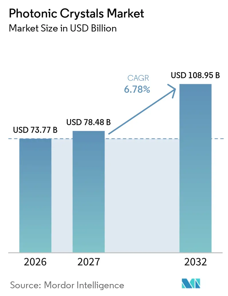
The Photonic Crystals Market size was valued at USD 73.77 billion in 2026 and is estimated to grow from USD 78.48 billion in 2027 to reach USD 108.95 billion by 2032, at a CAGR of 6.78% during the forecast period (2027-2032). Demand from artificial intelligence data centers, factory automation, and optical sensing is moving the photonic crystals market beyond its earlier telecommunications focus. These applications need components that manage light precisely while limiting thermal loss and power use. Public programs in the United States, Europe, Israel, and Canada are reducing the financial risk of scaling production. This support is creating opportunities within the photonic crystals market for suppliers that can combine specialized designs with manufacturable processes. Established optical component groups hold strong positions, while specialized fiber and artificial intelligence optics suppliers are competing for demanding applications.
Key Report Takeaways
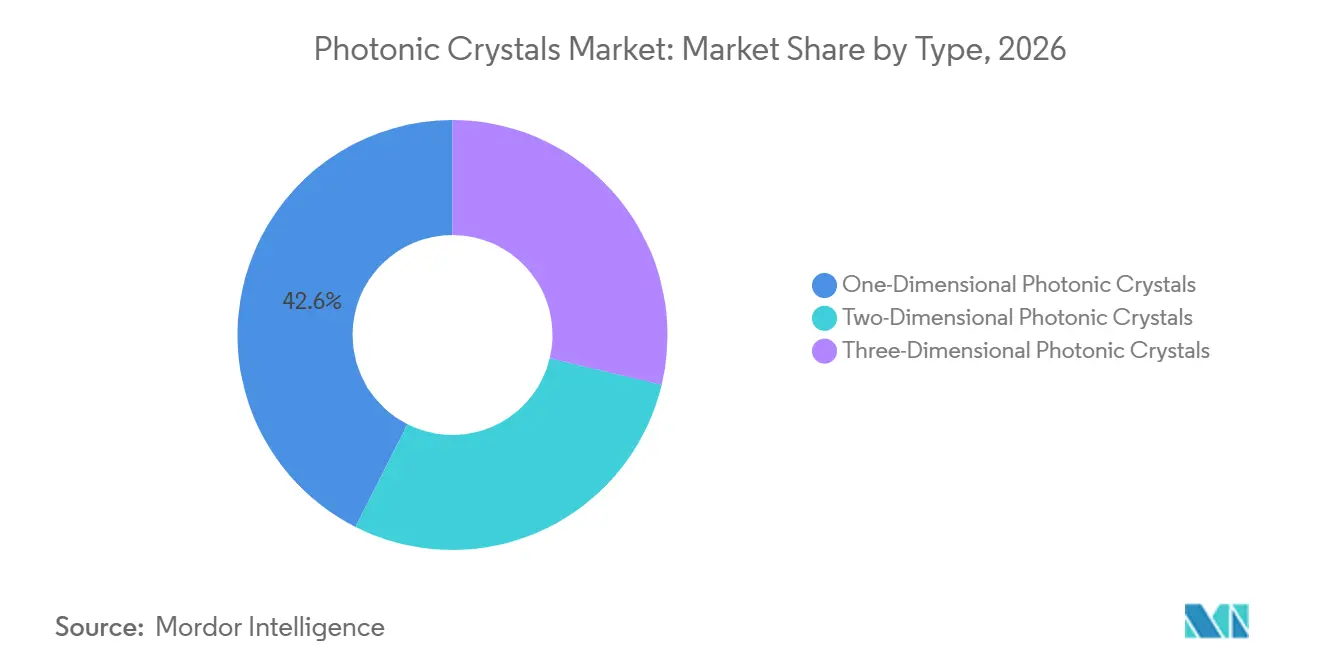
- By type, one-dimensional photonic crystals held 42.56% of the photonic crystals market share in 2026, while two-dimensional photonic crystals are forecast to advance at a 7.13% CAGR through 2032.
- By application, optical fibers held 34.82% of the photonic crystals market share in 2026, while light-emitting diodes and displays are forecast to advance at a 7.48% CAGR through 2032.
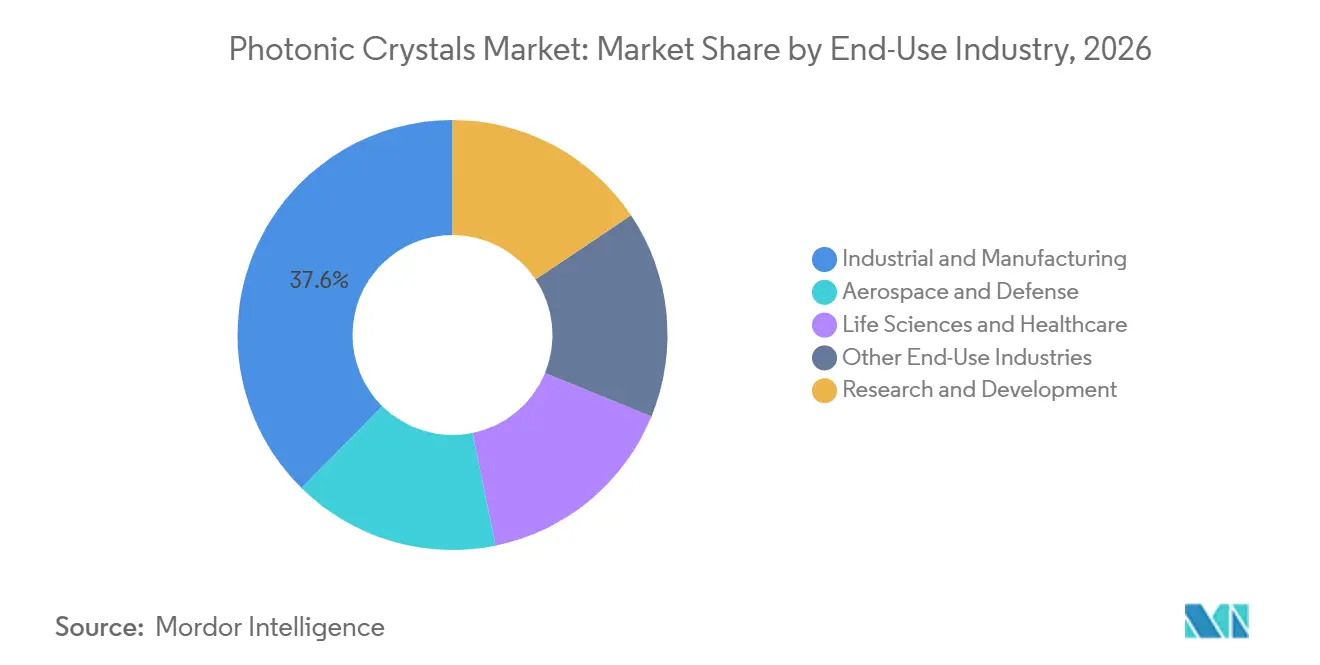
- By end-use industry, industrial and manufacturing held 37.61% of the photonic crystals market share in 2026, while aerospace and defense are forecast to advance at a 7.79% CAGR through 2032.
- By geography, Asia-Pacific held 38.36% of the photonic crystals market share in 2026 and is forecast to advance at a 7.51% CAGR through 2032.
Note: Market numbers in this report are based on Mordor Intelligence's proprietary estimation framework, which combines nine months of actuals with Q4 projections for base year 2026.
Market Trends and Insights
Drivers Impact Analysis of Photonic Crystals Market*
| Driver | (~) % Impact on CAGR Forecast | Geographic Relevance | Impact Timeline |
|---|---|---|---|
| Demand for Higher Data Rates in Optical Communications | +2.5% | Global, concentrated near-term pull in North America and APAC core | Short term (≤ 2 years) |
| Energy-Efficient Light Management in LEDs and Solar Cells | +1.8% | Global, primary gains in Asia-Pacific and North America | Medium term (2-4 years) |
| Expansion of Photonic Sensing in Industrial and Healthcare Applications | +1.2% | Global, early momentum in Europe and APAC | Medium term (2-4 years) |
| Government and Private Investment in Quantum and Integrated Photonics | +1.0% | North America, Europe, with spillover to Israel, Canada, APAC | Long term (≥ 4 years) |
| Reuse of Silicon-Photonics Manufacturing Infrastructure for Photonic-Crystal Devices | +0.8% | North America & Europe, with spillover to APAC foundries | Medium term (2-4 years) |
| Source: Mordor Intelligence | |||
Demand for Higher Data Rates in Optical Communications
Artificial intelligence data center projects are raising optical interface requirements from 400G toward 1.6T per lane, which increases demand for photonic crystal fiber with high bandwidth and low nonlinearity. The photonic crystals market is increasingly connected to data center network planning. In May 2026, Corning Incorporated and NVIDIA announced a multiyear partnership under which Corning Incorporated plans to expand United States optical connectivity manufacturing capacity by 10x and fiber production by more than 50%, including 3 planned plants in North Carolina and Texas. In March 2026, Lumentum Operations LLC announced a strategic partnership with NVIDIA to develop optics technology for artificial intelligence infrastructure. Research presented at the Optical Fiber Communication Conference in 2025 showed that photonic crystal nanobeam cavities with quality factors above 150,000 can be made on AIM Photonics’s standard 300 mm silicon nitride platform. The combination of capacity investment and process validation is shortening the route to commercial data center use in the photonic crystals market.
Energy-Efficient Light Management in LEDs and Solar Cells
Photonic crystal nanostructures can improve how light is emitted from light-emitting diodes (LEDs) and absorbed by solar cells. The photonic crystals market also benefits when energy use becomes a more important product requirement. A 2025 study reported a certified 23.1% silicon solar cell efficiency after integrating laser-patterned photonic crystal light-trapping structures while maintaining strong surface passivation. A 2025 Scientific Reports study found that nano-patterned sapphire substrates and reflecting photonic crystals in aluminum gallium nitride ultraviolet B LEDs improved light extraction by 150%, addressing external quantum efficiency below 15%. International Electrotechnical Commission 62788 standards for photovoltaic module components and European Union energy-labeling rules are supporting interest in more efficient cell architectures. Suppliers that integrate these structures into existing production lines may be better placed to serve building-integrated photovoltaic projects.
Expansion of Photonic Sensing in Industrial and Healthcare Applications
Photonic crystal fiber sensors combine high sensitivity, compact dimensions, and resistance to electromagnetic interference. The photonic crystals market can draw demand from both medical testing and industrial monitoring. A 2025 Scientific Reports paper described a two-dimensional photonic crystal biosensor for urine glucose with sensitivity of 20,040.30 nm/RIU and a detection limit of 8×10⁻¹⁰. A December 2025 review in IEEE Sensors Journal reported that photonic crystal fiber biosensors can detect chemical compounds and bacterial pathogens with high specificity from 1 THz to 2.6 THz. In industrial settings, distributed sensing can support structural monitoring, gas leak detection, and process temperature mapping where electronic sensors face heat or interference. The use of these technologies in healthcare diagnostics and industrial process control can limit exposure to downturns in a single end-use area.
Government and Private Investment in Quantum and Integrated Photonics
Public investment in photonic quantum computing is increasing demand for high-performance photonic crystal components. The photonic crystals market benefits as programs support both research and industrial manufacturing. In September 2026, the U.S. Department of Commerce finalized a CHIPS and Science Act award of up to USD 100 million to PsiQuantum for low-loss photonic packaging and electro-optic materials[1]. The European Commission signed the Photonics for Quantum Pilot Line project in July 2026, with a total cost of EUR 51.5 million (approximately USD 56.3 million), to build manufacturing infrastructure involving IMEC, TU Delft, VTT, Leonardo, and 25 additional institutions. Canada entered negotiations in March 2026 to provide Xanadu Quantum Technologies Inc. up to CAD 390 million (approximately USD 281.6 million) for Project OPTIMISM, while Israel launched an NIS 150 million (approximately USD 41 million) initiative for integrated photonics infrastructure in June 2026. These programs support the photonic crystals market by addressing design, prototyping, packaging, and the move toward volume manufacturing.
Restraints Impact Analysis of Photonic Crystals Market*
| Restraint | (~) % Impact on CAGR Forecast | Geographic Relevance | Impact Timeline |
|---|---|---|---|
| Fabrication Complexity and Yield Loss in Higher-Dimensional Structures | -1.5% | Global, acute impact in R&D-heavy markets: North America, Europe, APAC | Medium term (2-4 years) |
| High Cost of Precision Nanofabrication, Packaging, and Optical Testing | -1.2% | Global, disproportionately affecting smaller players and emerging markets | Long term (≥ 4 years) |
| Limited Standardization Across Photonic-Crystal Materials and Device Architectures | -0.7% | Global, acute impact in regulated sectors: aerospace, healthcare | Long term (≥ 4 years) |
| Source: Mordor Intelligence | |||
Fabrication Complexity and Yield Loss in Higher-Dimensional Structures
Three-dimensional photonic crystals and advanced two-dimensional designs need fabrication tolerances below 100 nm. Sidewall roughness, micromasking during reactive ion etching, and etch variation can lower cavity quality factors and weaken photonic bandgaps. Research discussed at a 2025 quantum conference showed that such defects reduced the quality factor of diamond photonic crystal cavities and limited their scale-up for quantum networks. A 2025 Nature Communications study showed that transfer-printing micro-assembly can characterize, sort, and rearrange cavity pixels, including 119 devices in 1 session. The method adds production steps rather than removing the core yield problem. Yield loss will continue to limit the addressable demand for high-dimensional structures until fine-feature uniformity improves at production scale.
High Cost of Precision Nanofabrication, Packaging, and Optical Testing
Electron beam lithography and extreme ultraviolet lithography are important patterning tools for nanoscale photonic crystal features. Their equipment and operating costs restrict use to applications where higher performance supports the cost. A 2025 study on photonic metamaterial manufacturing identified persistent difficulty in achieving precision registration across wide fields at economically viable throughput. The lack of unified photonic crystal fiber test protocols under International Electrotechnical Commission (IEC) Technical Committee 86 requires tailored qualification work in conservative sectors. Medical devices must meet International Organization for Standardization 13485 requirements, aerospace components need military specifications, and telecommunications components must align with International Telecommunication Union Telecommunication Standardization Sector G-series recommendations. Larger integrated manufacturers can absorb these costs more easily because they already operate fabrication and testing infrastructure.
*Our forecasts treat driver/restraint impacts as directional, not additive. The impact forecasts reflect baseline growth, mix effects, and variable interactions.
Photonic Crystals Market Segment Analysis
By Type:
One-Dimensional Photonic Crystals Anchor Revenue, While Two-Dimensional Photonic Crystals ExpandOne-dimensional photonic crystals held 42.56% of the photonic crystals market size by type in 2026. The photonic crystals market continues to rely on these structures because they are compatible with established deposition processes used for fiber, coatings, solar cells, and aerospace thermal management. Research published in 2025 found that silicon and silicon dioxide one-dimensional stacks achieved average infrared emissivity as low as 0.076 in the 3-5 µm band. Three-dimensional photonic crystals remain the smallest revenue category but are important for quantum optics because a complete three-dimensional bandgap can prevent unwanted spontaneous emission.
Two-dimensional photonic crystals are projected to advance at a 7.13% CAGR through 2032. Photonic crystal surface-emitting laser platforms are approaching 50 W of coherent output from a single device, according to a 2026 Japan Science and Technology Agency review. Two-dimensional biosensor designs have also demonstrated urine glucose detection at 8×10⁻¹⁰ mol/L, and transfer-printing can help create cavity arrays with controlled resonant wavelengths. Hamamatsu Photonics K.K. identified photonic crystal fiber as an enabling technology for kilowatt-class industrial and security laser systems in its March 2026 briefing. As foundry-scale costs decline, demand is expected to shift toward higher-dimensional designs.

By Application:
Optical Fibers Define Revenue, While Light-Emitting Diodes and Displays Grow FastestOptical fibers held 34.82% of the photonic crystals market size by application in 2026. The photonic crystals market uses fiber designs where conventional step-index products cannot meet performance requirements, including polarization-maintaining, large-mode-area, and hollow-core designs. In March 2025, Fujikura Ltd. began sample shipments of TitaniaBend PANDA polarization-maintaining fiber, jointly developed with Corning Incorporated, for 800 Gbit/s transceivers. In March 2026, Fujikura Ltd. commercialized a 4,000-fiber cable for Japanese data centers that fits 4,000 fibers within a 23 mm outer diameter.
Light-emitting diodes and displays are projected to advance at a 7.48% CAGR through 2032. A 2025 study found that combined nano-patterned sapphire and reflecting photonic crystals improved light extraction by 150% in aluminum gallium nitride ultraviolet B LEDs. Solar and photovoltaic cells can use photonic crystal light trapping, as demonstrated by the certified 23.1% silicon cell result. Image sensors can use two-dimensional photonic crystal polarization filters for single-exposure angle-resolved imaging. Lasers, supercontinuum sources, and discrete and integrated optical components serve precision measurement, biomedical imaging, and wavelength management needs.
By End-Use Industry:
Industrial and Manufacturing Anchors Revenue, While Aerospace and Defense Drive GrowthIndustrial and manufacturing held 37.61% of the photonic crystals market share in 2026. The photonic crystals market draws repeat industrial demand through precision laser machining, machine vision, and distributed sensing in semiconductor plants, automotive assembly, and power generation. Hamamatsu Photonics K.K. reported that its laser segment, where photonic crystal fiber is a core technology, targets a 16.7% revenue CAGR from fiscal year 2025 to fiscal year 2028. Gooch & Housego PLC and MKS Instruments, Inc. provide precision photonic components and optical instruments, where reliable supply and qualification records are important.
Aerospace and defense is projected to advance at a 7.79% CAGR through 2032. In 2025, the U.S. Air Force awarded Heroica Technologies LLC a Phase II Small Business Innovation Research contract of USD 1.8 million for lens-embedded photonic crystal mid-wave infrared imaging systems[2]. The company stated that the systems can offer a 1,000x size and weight reduction over conventional refractive optics for small, unmanned platforms. A 2025 study reported a one-dimensional photonic crystal stealth material with a 4.95 GHz radar absorption bandwidth and average infrared emissivity of 0.1063. Life sciences and healthcare are also adopting biosensors, while research and development remains an important buyer through quantum computing programs.
Geography Analysis
APAC Photonic Crystals Market
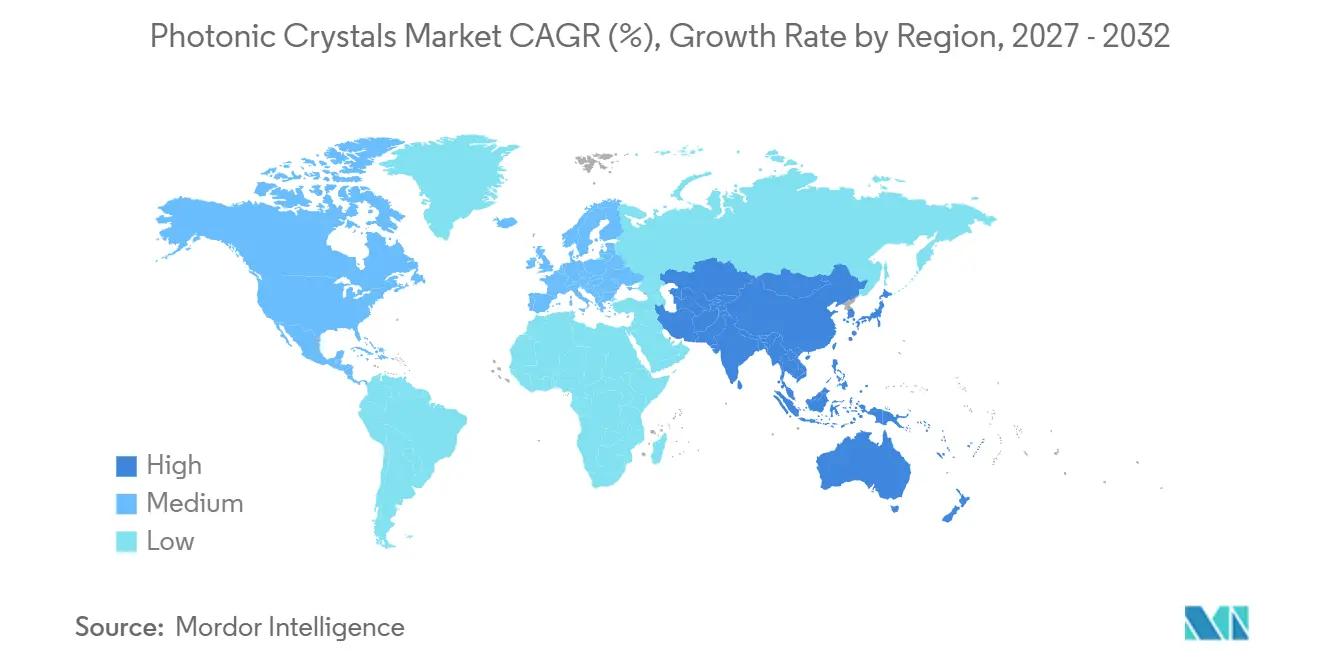
Asia-Pacific held 38.36% of the photonic crystals market share in 2026 and is projected to advance at a 7.51% CAGR through 2032. The photonic crystals market has a strong regional base in Asia-Pacific because of China’s optical manufacturing, Japan’s compound semiconductor capability, and South Korea’s display investments. A 2026 Japan Science and Technology Agency review stated that Japanese indium phosphide optical device makers held 50% of the advanced data center photonic component sector. Chinese suppliers are moving toward hollow-core and nonlinear fiber designs for 5G, 6G, and artificial intelligence data center links. South Korea’s investment in mini light-emitting diode and micro light-emitting diode architectures expands demand for display applications.
North America Photonic Crystals Market
North America is a leading regional base for photonic quantum computing, co-packaged optics, and aerospace photonics. Corning Incorporated’s planned United States capacity expansion and multiyear NVIDIA partnership are intended to raise domestic connectivity manufacturing capacity. Lumentum Operations LLC’s partnership with NVIDIA reflects investment in advanced optics for artificial intelligence systems. Canada is developing a quantum manufacturing base through Project OPTIMISM for photonic integrated circuit packaging and quantum-module assembly.
EMEA and South America Photonic Crystals Market
Europe retains research and specialty manufacturing capability in Germany, the United Kingdom, France, and the Nordic countries. STMicroelectronics and IMEC are supporting the STARLight consortium’s 300 mm silicon photonics line for artificial intelligence, data center, telecommunications, and automotive applications through 2028. The Photonics for Quantum Pilot Line provides distributed manufacturing for quantum-grade photonic integrated circuits. South America remains linked to telecommunications expansion in Brazil and Argentina. The Middle East and Africa is at an early stage of adoption as fiber networks become denser.
Competitive Landscape
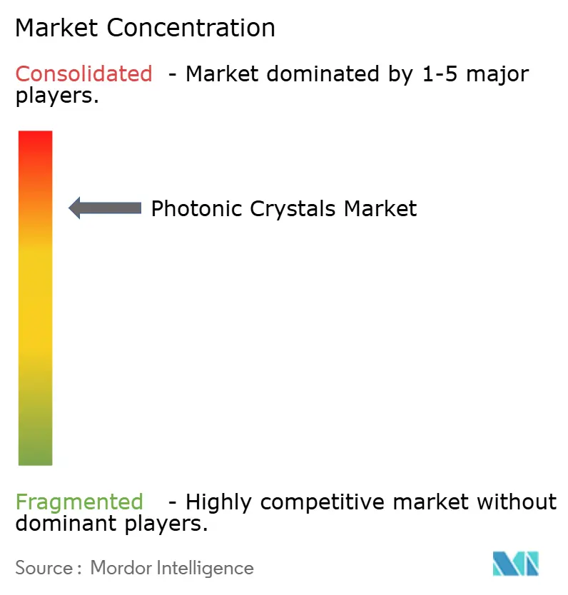
The photonic crystals market is consolidated, with the top five players including Photonic Lattice, Inc., Corning Incorporated, GLOphotonics, Exail, and Shanghai Precilasers Technology Co., Ltd. Competition has increased as artificial intelligence infrastructure customers form direct relationships with optical component manufacturers. In March 2026, Lumentum Operations LLC announced a strategic partnership with NVIDIA for advanced optics technology. In May 2026, Corning Incorporated announced its NVIDIA partnership and plans for 3 plants in North Carolina and Texas, while specialty producers such as GLOphotonics and Photonic Lattice, Inc. compete in quantum photonics and ultraviolet illumination.
OFS Fitel, LLC has pursued intellectual property for radiation-hardened photonic crystal fiber and enhanced back-scattering fiber networks for nuclear monitoring and distributed sensing. Hamamatsu Photonics K.K. stated in March 2026 that photonic crystal fiber is a core enabling technology for kilowatt-class laser systems. Its June 2026 integration of the NKT Photonics subsidiary reflects a vertical approach to quantum, security, and industrial laser platforms. This strategy helps suppliers control component performance, manufacturing knowledge, and customer qualification. The photonic crystals market therefore rewards companies that can link materials capability with application-specific system knowledge.
Hollow-core photonic crystal fiber for low-latency communications and two-dimensional biosensors for portable diagnostics have room for new capacity. Luna Innovations Incorporated, Newport Corporation, and MKS Instruments, Inc. compete in precision instruments and sensing, where qualification portfolios and application expertise are important. Exail, Gooch & Housego PLC, Opalux Inc., and Shanghai Precilasers Technology Co., Ltd. also serve specialized optical and laser requirements. Fujikura Ltd. and FURUKAWA ELECTRIC CO., LTD. benefit from their fiber and cable experience, while IPG Photonics Corporation remains relevant to high-power fiber lasers. Pricing pressure is most likely in mature device categories, while advanced fiber and quantum photonics applications remain contested among specialized suppliers.
Photonic Crystals Industry Leaders
-
Photonic Lattice, Inc.
-
Corning Incorporated
-
GLOphotonics
-
Exail
-
Shanghai Precilasers Technology Co., Ltd.
- *Disclaimer: Major Players sorted in no particular order
Photonic Crystals Market Companies Covered in this Report
- Corning Incorporated
- Exail
- Fujikura Ltd.
- FURUKAWA ELECTRIC CO., LTD.
- GLOphotonics
- Gooch & Housego PLC
- Hamamatsu Photonics K.K.
- IPG Photonics Corporation
- Lumentum Operations LLC
- Luna Innovations Incorporated
- MKS Instruments, Inc.
- Newport Corporation
- OFS Fitel, LLC
- Opalux Inc.
- Photonic Lattice, Inc.
- Shanghai Precilasers Technology Co., Ltd.
Recent Industry Developments in Photonic Crystals Market
- September 2026: The U.S. Department of Commerce finalized a CHIPS and Science Act research and development award of up to USD 100 million to PsiQuantum for photonic quantum computing, covering ultra-low-loss photonic packaging and electro-optic materials. The award supports the photonic crystals market by advancing photonic integrated circuit technologies and materials needed for scalable quantum computing systems.
- July 2026: The European Commission launched the Photonics for Quantum Pilot Line project, with a total cost of EUR 51.5 million (approximately USD 56.3 million) and an EU contribution of EUR 24.9 million (approximately USD 27.2 million), to establish photonic integrated circuit manufacturing infrastructure for quantum applications through March 2029. The project supports the photonic crystals market by strengthening manufacturing and integration capabilities for advanced optical components used in quantum photonics.
Global Photonic Crystals Market Report Scope
Photonic crystals are engineered optical materials with periodic variations in refractive index that control the propagation of light across specific wavelengths. Their optical properties enable light manipulation and confinement in applications involving sensing, imaging, communications, and photonic devices.
The Photonic Crystals Market is segmented by type, application, end-use industry, and geography. By type, the market is segmented into one-dimensional photonic crystals, two-dimensional photonic crystals, and three-dimensional photonic crystals. By application, the market is segmented into optical fibers, light-emitting diodes and displays, image sensors, solar and photovoltaic cells, lasers and supercontinuum sources, discrete and integrated optical components, and other applications. By end-use industry, the market is segmented into industrial and manufacturing, aerospace and defense, life sciences and healthcare, research and development, and other end-use industries. The report also covers the market size and forecasts for photonic crystals across 15 countries. For each segment, the market sizing and forecasts have been done on the basis of value (USD).
Segmentation Overview
| One-Dimensional Photonic Crystals |
| Two-Dimensional Photonic Crystals |
| Three-Dimensional Photonic Crystals |
| Optical Fibers |
| Light-Emitting Diodes and Displays |
| Image Sensors |
| Solar and Photovoltaic Cells |
| Lasers and Supercontinuum Sources |
| Discrete and Integrated Optical Components |
| Other Applications |
| Industrial and Manufacturing |
| Aerospace and Defense |
| Life Sciences and Healthcare |
| Research and Development |
| Other End-Use Industries |
| Asia-Pacific | China |
| India | |
| Japan | |
| South Korea | |
| ASEAN Countries | |
| Rest of Asia-Pacific | |
| North America | United States |
| Canada | |
| Mexico | |
| Europe | Germany |
| United Kingdom | |
| France | |
| Italy | |
| NORDIC Countries | |
| Rest of Europe | |
| South America | Brazil |
| Argentina | |
| Rest of South America | |
| Middle East and Africa | Saudi Arabia |
| South Africa | |
| Rest of Middle East and Africa |
| By Type | One-Dimensional Photonic Crystals | |
| Two-Dimensional Photonic Crystals | ||
| Three-Dimensional Photonic Crystals | ||
| By Application | Optical Fibers | |
| Light-Emitting Diodes and Displays | ||
| Image Sensors | ||
| Solar and Photovoltaic Cells | ||
| Lasers and Supercontinuum Sources | ||
| Discrete and Integrated Optical Components | ||
| Other Applications | ||
| By End-Use Industry | Industrial and Manufacturing | |
| Aerospace and Defense | ||
| Life Sciences and Healthcare | ||
| Research and Development | ||
| Other End-Use Industries | ||
| By Geography | Asia-Pacific | China |
| India | ||
| Japan | ||
| South Korea | ||
| ASEAN Countries | ||
| Rest of Asia-Pacific | ||
| North America | United States | |
| Canada | ||
| Mexico | ||
| Europe | Germany | |
| United Kingdom | ||
| France | ||
| Italy | ||
| NORDIC Countries | ||
| Rest of Europe | ||
| South America | Brazil | |
| Argentina | ||
| Rest of South America | ||
| Middle East and Africa | Saudi Arabia | |
| South Africa | ||
| Rest of Middle East and Africa | ||
Key Questions Answered in the Report
What is the size of the photonic crystals market?
The photonic crystals market size was valued at USD 73.77 billion in 2026 and is estimated to grow from USD 78.48 billion in 2027 to reach USD 108.95 billion by 2032, at a CAGR of 6.78% during the forecast period (2027-2032).
What is driving demand for photonic crystals?
Artificial intelligence data center connections, efficient LEDs and solar cells, industrial sensing, and quantum photonics investment are supporting demand.
Which type held the largest share in 2026?
One-dimensional photonic crystals held 42.56% of the market share in 2026.
Which application is projected to advance fastest through 2032?
Light-emitting diodes and displays are projected to advance at a 7.48% CAGR through 2032, supported by improved light extraction in ultraviolet LEDs.