Millimeter-Wave Imaging For Industrial Inspection Market Size and Share
Market Overview
| Study Period | 2020 - 2031 |
|---|---|
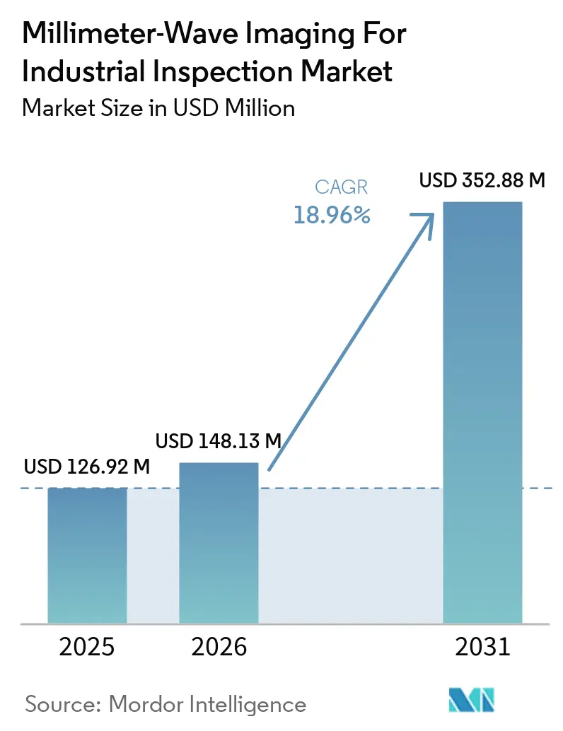
| Market Size (2026) | USD 148.13 Million |
| Market Size (2031) | USD 352.88 Million |
| Growth Rate (2026 - 2031) | 18.96 % |
| Fastest Growing Market | Asia-Pacific |
| Largest Market | Asia-Pacific |
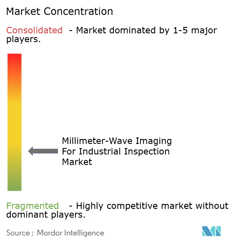
| Market Concentration | Medium |
Major Players *Disclaimer: Major Players sorted in no particular order Image © Mordor Intelligence. Reuse requires attribution under CC BY 4.0. | |
Millimeter-Wave Imaging For Industrial Inspection Market Analysis by Mordor Intelligence
The millimeter-wave imaging for industrial inspection market size is projected to expand from USD 126.92 million in 2025 and USD 148.13 million in 2026 to USD 352.88 million by 2031, registering a CAGR of 18.96% between 2026 and 2031. Manufacturers are replacing ionizing inspection methods with non-destructive millimeter-wave systems across food packaging and semiconductor fabrication. These systems can create volumetric 3D images without radiation hazards or damage to the inspected product. The image stacks also provide richer inputs for AI quality tools than 2D shadow images, so each inspection cycle can support later quality decisions. Zero-defect requirements from automotive and aerospace original equipment manufacturers, together with pharmaceutical packaging integrity requirements, are supporting the adoption of millimeter-wave imaging in the industrial inspection market. Suppliers are responding by combining RF hardware, image processing, AI software, and production-line interfaces in integrated offerings.
Key Report Takeaways
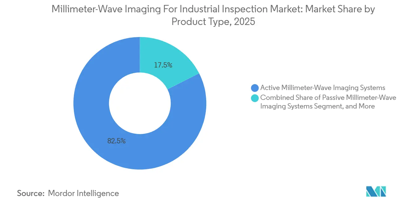
- By product type, active millimeter-wave imaging systems accounted for 82.47% of the revenue of the millimeter-wave imaging for industrial inspection market in 2025, while passive millimeter-wave imaging systems are projected to expand at a CAGR of 21.67% through 2031.
- By system format, integrated inline inspection systems held 38.73% of revenue of the millimeter-wave imaging for industrial inspection market in 2025, while handheld and portable inspection systems are projected to expand at a CAGR of 19.44% through 2031.
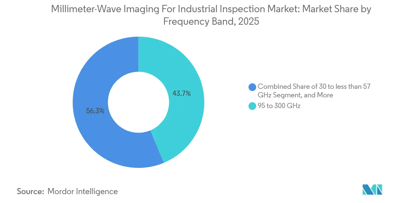
- By frequency band, the 95-300 GHz category accounted for 43.67% of the revenue of the millimeter-wave imaging for industrial inspection market in 2025, and is projected to expand at a CAGR of 2197% through 2031.
- By end-user industry, food and beverage accounted for 24.83% of revenue in 2025, while electronics and semiconductors are projected to expand at a CAGR of 19.28% through 2031.
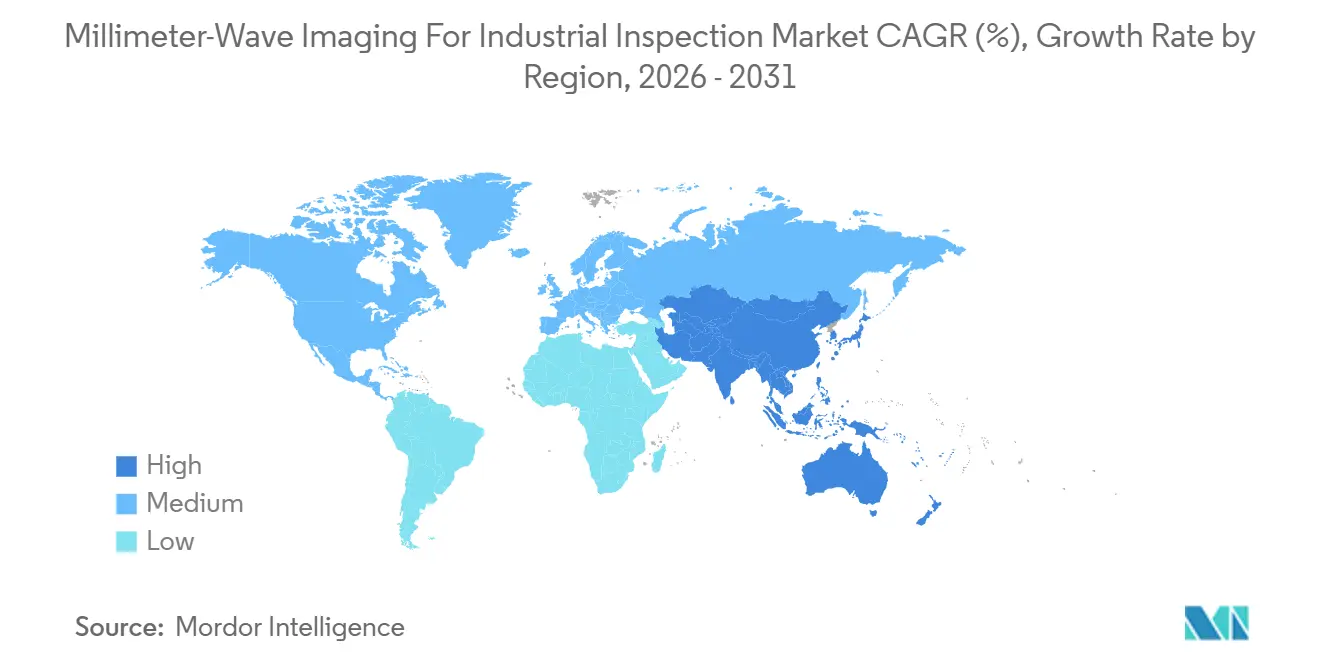
- By geography, Asia-Pacific accounted for 35.71% of revenue in 2025 and is projected to grow at a CAGR of 19.74% through 2031.
Note: Market size and forecast figures in this report are generated using Mordor Intelligence’s proprietary estimation framework, updated with the latest available data and insights as of January 2026.
Global Millimeter-Wave Imaging For Industrial Inspection Market Trends and Insights
Drivers Impact Analysis*
| Driver | (~) % Impact on CAGR Forecast | Geographic Relevance | Impact Timeline |
|---|---|---|---|
| Adoption of Non-Destructive Inline Quality Control | +4.8% | Global, with highest intensity in North America and Asia-Pacific | Short term (≤ 2 years) |
| Inspection of Sealed Packages Without Opening | +3.5% | Global, with strongest demand from European food and pharmaceutical OEMs | Short term (≤ 2 years) |
| Zero-Defect and Product-Safety Requirements | +2.9% | North America, Europe, and Asia-Pacific core markets | Medium term (2-4 years) |
| AI-Based Defect Recognition With Millimeter-Wave Images | +2.5% | Global, led by North America and China AI investment hubs | Medium term (2-4 years) |
| High-Throughput Automated Manufacturing Lines | +1.8% | Asia-Pacific core markets, with spillover to South America and Middle East and Africa | Medium term (2-4 years) |
| Multimodal Inspection for Composite and Dielectric Materials | +1.3% | North America and Europe aerospace and automotive clusters | Long term (≥ 4 years) |
| Source: Mordor Intelligence | |||
Increasing Adoption of Non-Destructive Inline Quality Control
Inline non-destructive testing has become more important where batch sampling cannot meet zero-defect expectations. Millimeter-wave systems support 100% inline inspection because they are contactless, non-ionizing, and can operate at conveyor speeds. This makes the millimeter-wave imaging for the industrial inspection market relevant to factories that need coverage without stopping material flow. Rohde and Schwarz introduced the R&S IMAGER in July 2026 with standard interfaces for connection to existing production-control software. The system allows engineers to extend volumetric inspection coverage without redesigning the wider manufacturing environment.[1]Rohde and Schwarz, “The R&S IMAGER from Rohde and Schwarz Uses Millimeter Wave Imaging to Inspect the Quality of Packaged Goods in Real Time,” Rohde and Schwarz, rohde-schwarz.com. A 2025 IEEE Access study reported automated near-field synthetic aperture radar defect localization across aerospace and automotive components, providing a production-focused reference point for this use.[2]Dongjie Bi et al., “Automated Internal Defect Identification and Localization Based on a Near-Field SAR Millimeter-Wave Imaging System,” IEEE Access, ieee.org.
Image retention adds a practical record-keeping benefit to inline inspection. Each millimeter-wave image can be retained as a traceable representation of the inspected item. That record can support quality reviews and electronic documentation obligations. The approach differs from inspection methods that only produce a 2D projection for an immediate pass-or-fail decision. The Ferdinand-Braun-Institut presented a 110 GHz line scanner in 2024 with 80 monolithically integrated detectors and readout speeds of up to 15,000 images per second. This demonstrated that imaging throughput need not be the main constraint for some inline applications in the millimeter-wave imaging for industrial inspection market.
Rising Need to Inspect Sealed Packages Without Product Opening
Food, pharmaceutical, and logistics operators need to verify packaged goods without opening them. Conventional cameras and weight-based tools cannot consistently assess the internal condition of a sealed item. Millimeter-wave signals can pass through cardboard, plastics, laminated films, and glass used in common packaging. They can support checks for product presence, seal defects, and missing components without direct contact. ThruWave states that its platform inspects sealed boxes at up to 600 feet per minute and 4 items per second. The operating case is strengthening the role of the millimeter-wave imaging for the industrial inspection market in package verification.
A 2025 ACM study examined through-package liquid leakage detection using millimeter-wave synthetic aperture radar imaging. The study reported accuracy above 93% for leakage detection and liquid identification, which was 14.70% higher than the baseline methods it evaluated.[3]“SARLiquid: Through-Package Liquid Leakage Detection Based on mmWave SAR Imaging,” Association for Computing Machinery, acm.org. This type of inspection addresses a gap where visual systems cannot see through packaging materials. Rohde and Schwarz also identified vacuum loss in sealed glass bottles as a condition that its system can detect. X-ray inspection cannot reliably identify this type of failure. The capability extends the use of millimeter-wave imaging beyond foreign-body screening and toward package-physics verification.
Tightening Zero-Defect and Product-Safety Requirements
Automotive suppliers operate under IATF 16949:2016 requirements, while aerospace suppliers work under AS9100D requirements. These frameworks increase attention to inspection methods that can cover all output rather than a sample. The millimeter-wave imaging for the industrial inspection market benefits when manufacturers need to document quality checks for every item. In pharmaceutical production, 21 CFR Part 11 requires electronic records to be attributable, legible, and suitable for audit. Volumetric image archives can help automated inspection systems provide those records.[4]US Food and Drug Administration, “Part 11, Electronic Records, Electronic Signatures, Scope and Application,” US Food and Drug Administration, fda.gov. Food-contact plastics obligations under Regulation (EU) No 10/2011 also favor documented, image-based inspection arrangements.
The European Medical Device Regulation requires documented design-verification records for products such as autoinjectors and prefilled syringes. Non-contact millimeter-wave inspection has specific relevance where internal assembly must be checked without harming the device. These requirements can make a qualified inline system difficult to replace. A manufacturer changing the installed inspection method may need to complete a new qualification process. That process raises the value of established installed bases in pharmaceutical and aerospace applications. It also makes early implementation an important commercial consideration in the millimeter-wave imaging for industrial inspection market.
Integration of AI-Based Defect Recognition With Millimeter-Wave Images
Deep learning is moving from research work toward deployed millimeter-wave inspection systems. In regulated settings, the ability to explain a result matters alongside raw detection accuracy. A 2025 IEEE Access study used explainable AI visual maps with millimeter-wave non-destructive testing to support weakly supervised defect localization. The approach can show the image regions associated with a defect finding. This helps address confidence concerns around opaque AI decisions. It also supports a more auditable workflow for millimeter-wave imaging in the industrial inspection market.
The R&S IMAGER produces high-contrast 3D images that can be handled as digital twins in AI fault-detection workflows. This configuration presents the machine as a source of usable production data rather than only an inspection device. ThruWave states that its algorithms use more than 20 million millimeter-wave images collected in production environments. Such training data is difficult for hardware-only suppliers to reproduce without sustained deployment. Patent activity also covers probe arrays embedded in semiconductor tools with machine learning classifiers for process-defect detection. The combination of image data, classifiers, and system deployment is shaping competition in the millimeter-wave imaging for industrial inspection market.
Restraints Impact Analysis*
| Restraint | (~) % Impact on CAGR Forecast | Geographic Relevance | Impact Timeline |
|---|---|---|---|
| High System and Integration Costs | -2.5% | Global, especially South America, Middle East and Africa, and small and mid-size manufacturers | Short term (≤ 2 years) |
| Limited Penetration Through Water-Rich and Conductive Materials | -1.7% | Global, limiting fresh food and metallic enclosure inspection | Medium term (2-4 years) |
| Calibration Complexity and Application-Specific Model Training | -1.1% | Global, especially for new entrants in electronics and semiconductor applications | Medium term (2-4 years) |
| Fragmented Industrial Inspection Validation Standards | -0.8% | Global, delaying procurement in pharmaceutical, aerospace, and defense applications | Long term (≥ 4 years) |
| Source: Mordor Intelligence | |||
High System and Integration Costs
A fully configured inspection cell requires multichannel transceiver arrays, signal processing, AI analytics software, and mechanical integration with the production line. This capital requirement can be difficult for small and mid-size manufacturers to justify. Systems operating from 95 GHz to 300 GHz rely on specialized compound semiconductor processes and precision waveguide components. Their component costs are structurally higher than those of optical camera systems based on commoditized CMOS sensors. The millimeter-wave imaging for the industrial inspection market also requires integration work to connect scanner outputs with manufacturing execution and production-control software. This work can require inspection-cell revalidation.
ThruWave completed an integration of Maple Systems' cMT3000 series human-machine interfaces in August 2025. The deployment supported multi-PLC communication and configurable interfaces, showing the practical effort needed in varied production environments. Existing X-ray systems, therefore, retain an advantage in price-sensitive environments. Chip-level integration from Qorvo and Sivers Semiconductors is narrowing part of the cost difference. However, hardware savings do not eliminate the costs of software integration, line installation, and process validation. These considerations can delay adoption even where the inspection capability is technically suitable.
Limited Penetration Through Water-Rich and Highly Conductive Materials
Millimeter-wave signals lose strength in materials with high free-water content. Metallic substrates reflect incident waves rather than transmit them. These physical limits cannot be fully removed through engineering changes. Fresh meat, high-moisture bakery products, and liquid-filled open containers are poor candidates for transmission-mode inspection. The addressable food applications are therefore concentrated in sealed, dry, or moderate-moisture products. This material constraint limits millimeter-wave imaging in the industrial inspection market in certain settings.
TeraSense reported strong terahertz imaging results for lactose powder while noting that high-moisture products substantially attenuate the signal. In electronics, dense copper interconnects and metal enclosures constrain subsurface imaging. Inspection is most useful for defects in accessible dielectric or polymer layers. This means millimeter-wave methods do not replace every PCB-level inspection technique. Calibration and application-specific model training can add complexity for newer suppliers. The lack of a dedicated IEC or ISO validation standard for industrial production lines also leaves buyers without a shared third-party benchmark, while IEC 63391:2024 addresses security screening of people rather than industrial inspection.
*Our forecasts treat driver/restraint impacts as directional, not additive. The impact forecasts reflect baseline growth, mix effects, and variable interactions.
Segment Analysis
By Product Type: Active Systems Anchor Revenue as Passive Variants Accelerate
Active millimeter-wave imaging systems held 82.47% of the millimeter-wave imaging for industrial inspection market share in 2025. Their built-in illumination source provides consistent image contrast on production floors. This is useful where ambient thermal conditions vary during a production run. Pharmaceutical, food, and electronics manufacturers use active designs for predictable image quality at operating speed. Consistent images can also reduce the need for manual recalibration before AI classification. The R&S IMAGER uses its own millimeter-wave source to transmit through packaging and reconstruct subsurface images through a sensor array. Its ISAR-based volumetric reconstruction supports the digital-twin format used in its output. This active architecture fits controlled production-floor environments where consistent coverage is important.
Passive millimeter-wave imaging systems are projected to expand at a CAGR of 19.23% through 2031. Logistics operators can use them where ambient thermal contrast provides enough information for anomaly detection. Passive systems avoid an active source and can suit situations with lower cost expectations. Their image quality depends more directly on the thermal contrast of the inspected product and its surroundings. This limits use where the environment does not provide clear contrast. TeraSense has described a move toward silicon-based sub-terahertz detector fabrication that would combine detection and signal processing on one chip. That approach can narrow the image-quality gap with active systems while reducing hardware cost. It supports a broader range of lower-cost inspection deployments in the millimeter-wave imaging for industrial inspection market.



By System Format: Portable Systems Expand Alongside an Inline Base
Integrated inline inspection systems accounted for 38.73% of the millimeter-wave imaging market share for industrial inspection in 2025. Food, pharmaceutical, and electronics original equipment manufacturers install these systems directly on conveyor-based lines. The format supports 100% throughput inspection when the process flow is stable. It is suited to factories that need continuous coverage of packaged goods or standardized components. The integration can connect images to production control systems and downstream handling decisions. It can also retain image records for later quality review. This combination makes inline systems the largest format, even though installation can require specialized engineering. The format remains central to the millimeter-wave imaging for the industrial inspection market, where product geometry and throughput suit conveyance.
Handheld and portable inspection systems are projected to expand at a CAGR of 19.44% through 2031. Construction, infrastructure, and logistics use cases often occur outside a fixed production line. Engineers can use portable scanners for concrete structures, composite panels, and building facades. A 2026 study assessed millimeter waves for non-destructive quality analysis of fiber-based panels during production stages. This supports the technical basis for field deployment. Standalone systems retain a role for aerospace and automotive components that do not fit a conveyor. The November 2024 expansion of the FieldFox handheld analyzer series to 170 GHz increased portable sub-terahertz coverage for field users. Portability therefore extends inspection to sites with varying part sizes and access conditions.
By Frequency Band: Sub-Terahertz Use Reflects Precision Requirements
The 95-300 GHz band held 43.67% of the millimeter-wave imaging for industrial inspection market share in 2025, and is projected to expand at a CAGR of 19.63% through 2031. This frequency range can deliver sub-millimeter spatial resolution. Semiconductor substrates, pharmaceutical packages, and autoinjector assemblies require this level of precision. A 2025 study demonstrated that optimized millimeter-wave SAR imaging detected surface defects as small as 0.4 mm. It included bonded adhesive lines on low-reflectivity materials. These results support the position of the 95-300 GHz band in precision manufacturing applications. The band is therefore important, where small surface features must be distinguished in a repeatable inspection sequence.
The 57 GHz to less than 95 GHz range offers a balance between penetration depth and resolution. It is suitable for automotive components and construction materials where subsurface reach is more important than very small surface detail. The 30 GHz to less than 57 GHz range provides the greatest penetration depth among the listed bands. It remains relevant for thick composite structures and precast concrete. Lower resolution is accepted in return for deeper imaging reach. A 2025 study validated near-field phase imaging at 30-40 GHz for glass fiber-reinforced plastics. IEC 63616:2025 provides a reference for conductivity measurement of metal thin films at microwave and millimeter-wave frequencies. Together, the frequency ranges allow the millimeter-wave imaging for industrial inspection market to address differing requirements for resolution, penetration, and material type.
By End-User Industry: Food Safety and Electronics Fabrication Shape Demand
Food and beverage held 24.83% of the millimeter-wave imaging for industrial inspection market share in 2025. The segment requires checks of sealed-package integrity and foreign bodies without product damage. Its compliance value includes the detection of vacuum loss in sealed glass bottles. This failure can be difficult for X-ray inspection to identify reliably. A compact 100 GHz millimeter-wave system demonstrated real-time foreign-body detection in chocolates moving on a conveyor during a 2025 study. The system operated at 5,000 frames per second. This demonstrates that food inspection can operate at production speed. The food and beverage segment remains a major source of demand for the millimeter-wave imaging for industrial inspection market.
Electronics and semiconductor is projected to expand at a CAGR of 19.28% through 2031. The segment uses millimeter-wave probe arrays in fabrication equipment to identify conductor and dielectric defects. This can address some defects outside the reach of automated optical inspection. Probe arrays assess changes in backscattered RF reflections from substrate conductor misalignment and via-pad defects. Embedded machine-learning classifiers can sort these changes during the process. Pharmaceutical inspection focuses on autoinjector and syringe assembly verification. Logistics and postal operators use the technology for sealed-parcel contraband detection. Aerospace and defense applications address composite-panel delamination and bonding defects. Construction, building materials, and general manufacturing use portable systems for structural field assessments.
Geography Analysis
Asia-Pacific held 35.71% of the millimeter-wave imaging for industrial inspection market share in 2025 and is projected to expand at a CAGR of 19.74% through 2031. China’s electronics assembly, food processing, and pharmaceutical contract manufacturing base supports regional demand. Government quality-infrastructure investment is also encouraging automated throughput inspection in place of visual sampling. Japan’s automotive supply chains operate under zero-defect requirements linked to IATF 16949. These requirements support inspection of EV battery components and power electronics. South Korea’s DRAM and NAND flash capacity expansion is increasing the need for substrate-defect screening. Millimeter-wave probe-based non-destructive testing can offer a practical alternative when X-ray computed tomography requires substantial computational resources.
North America is the second-largest regional area in the millimeter-wave imaging for industrial inspection market. Pharmaceutical, logistics, and aerospace applications support demand across the region. ThruWave operates from Seattle and provides automated mail contraband detection for parcels, flats, and envelopes without ionizing radiation. FAA guidance on composite structure inspection and US Department of Defense non-destructive evaluation standards support aerospace activity in US manufacturing clusters. Canada’s automotive corridor provides additional use cases. Mexico’s electronics assembly base also contributes to regional demand. These applications link product integrity, package screening, and composite inspection across North America.
Europe has strong industrial metrology capability and a high density of quality standards. Germany benefits from the presence of Rohde and Schwarz and a large automotive and capital-goods manufacturing base. France includes Teratonics SAS, Optikan SAS, and MC2 Technologies SAS in its developing inspection cluster. The United Kingdom contributes Farran Technology’s waveguide component experience. South America’s near-term demand centers on Brazil’s food processing and pharmaceutical sectors, where export compliance supports interest in validated inline inspection. Middle East and Africa remains at an earlier stage, although industrial diversification in the United Arab Emirates and Saudi Arabia’s Vision 2030 present longer-term opportunities. African activity is concentrated in research institutes and testing laboratories.

Competitive Landscape
The millimeter-wave imaging for industrial inspection market is moderately fragmented across RF components, inspection systems, and research-to-product specialists. RF component and chip suppliers include Virginia Diodes, Eravant, QuinStar Technology, SAGE Millimeter, Qorvo, Sivers Semiconductors, ACST GmbH, and RPG Radiometer Physics GmbH. System integrators and platform vendors include Rohde and Schwarz, ThruWave, TeraSense Group, Malcam, HÜBNER GmbH and Co. KG, Heliotis AG, and Vayyar Imaging. Research-to-product specialists include Optikan SAS, Teratonics SAS, Lytid AS, Millimeter Wave Products, Farran Technology, and MC2 Technologies SAS. These groups occupy different parts of the value chain rather than competing through one uniform product offer. The structure gives system providers access to application-specific RF elements without requiring all component design to be performed internally. It also means that production software, AI models, and integration capability can influence supplier selection.
Rohde and Schwarz launched the R&S IMAGER in July 2026. The system combines ISAR-based processing, AI-enabled volumetric imaging, and production-control software integration. The move shows an established RF instrument supplier extending into a complete inspection platform. ThruWave differentiates through algorithms that use more than 20 million production-environment images. Its approach combines image data, AI analytics, and high-throughput parcel inspection. TeraSense Group and Lytid AS are working toward lower-cost silicon-based detector solutions. This could move competition toward software and integration as hardware barriers decline.
Construction and building materials remain less served than food, pharmaceutical, logistics, and electronics applications. Portable systems for tunnels, bridges, and precast panels remain a potential area for specialized deployment. Malcam has installed more than 200 microwave moisture and density analyzer systems in tobacco and synthetic-fiber settings. This illustrates how a specialist position can create durable customer relationships in a defined vertical. Patent activity is also becoming more important as suppliers embed AI classification within inspection system designs. Industrial validation standards will influence purchasing once common IEC and ISO benchmarks become available. A market concentration score of 3 out of 10 applies because no combined share for the top players is provided, while the broad mix of component suppliers, integrators, and specialists indicates a fragmented competitive structure.
Millimeter-Wave Imaging For Industrial Inspection Industry Leaders
L3Harris Technologies, Inc.
Smiths Group plc
OSI Systems, Inc.
Rohde & Schwarz GmbH & Co. KG
ThruWave, Inc.
- *Disclaimer: Major Players sorted in no particular order

Recent Industry Developments
- July 2026: Rohde and Schwarz launched the R&S IMAGER, a real-time millimeter-wave packaged-goods scanner that penetrates common packaging materials at production speed without X-rays and generates high-contrast 3D digital-twin images for AI-powered fault detection across pharmaceutical, logistics, and food and beverage verticals.
- March 2026: Sivers Semiconductors announced general availability of its Daybreak 5G/6G Advanced ICs for FR3 7-15 GHz beamforming applications and multi-function defense arrays, expanding the frequency coverage of its commercially available millimeter-wave transceiver portfolio.
- February 2026: Sivers Semiconductors announced general availability of its Cloudchaser beamforming chipset and Maverick Ka-band antenna array panels for SATCOM ground terminals, advancing its production-ready millimeter-wave hardware platform for industrial system integrators.
- January 2026: Sivers Semiconductors secured an USD 800,000 development contract from a leading US defense contractor to apply its millimeter-wave beamformer technology in tactical communications programs, validating the defense-grade performance of its transceiver platform.


Global Millimeter-Wave Imaging For Industrial Inspection Market Report Scope
Millimeter-Wave Imaging for Industrial Inspection Market refers to non-contact, non-ionizing imaging systems that use electromagnetic waves in the 30-300 GHz (mmWave) range to inspect internal structure, thickness, and defects in dielectric and composite materials.
The Millimeter-Wave Imaging for Industrial Inspection Market Report is Segmented by Product Type (Active, and Passive), System Format (Benchtop/Lab, Handheld and Portable, Standalone, and Integrated Inline), Frequency Band (30 to less than 57 GHz, 57 to less than 95 GHz, and 95 to 300 GHz), End-User Industry (Food and Beverage, Pharmaceutical, Logistics, Postal and E-Commerce, Aerospace and Defense, Automotive and Transportation, Electronics and Semiconductor, Construction and Building Materials, General Manufacturing and Consumer Goods, Research Institutes and Testing Laboratories, and Other End-User Industries), and Geography (North America, South America, Europe, Asia-Pacific, and Middle East and Africa). The Market Forecasts are Provided in Terms of Value (USD).
| Active Millimeter-Wave Imaging Systems |
| Passive Millimeter-Wave Imaging Systems |
| Benchtop/Laboratory Inspection Systems |
| Handheld and Portable Inspection Systems |
| Standalone Inspection Systems |
| Integrated Inline Inspection Systems |
| 30 to less than 57 GHz |
| 57 to less than 95 GHz |
| 95 to 300 GHz |
| Food and Beverage |
| Pharmaceutical |
| Logistics, Postal and E-Commerce |
| Aerospace and Defense |
| Automotive and Transportation |
| Electronics and Semiconductor |
| Construction and Building Materials |
| General Manufacturing and Consumer Goods |
| Research Institutes and Testing Laboratories |
| Other End-User Industries |
| North America | United States | |
| Canada | ||
| Mexico | ||
| South America | Brazil | |
| Argentina | ||
| Rest of South America | ||
| Europe | Germany | |
| United Kingdom | ||
| France | ||
| Italy | ||
| Spain | ||
| Rest of Europe | ||
| Asia-Pacific | China | |
| Japan | ||
| India | ||
| South Korea | ||
| ASEAN | ||
| Rest of Asia-Pacific | ||
| Middle East and Africa | Middle East | Saudi Arabia |
| United Arab Emirates | ||
| Turkey | ||
| Rest of the Middle East | ||
| Africa | South Africa | |
| Nigeria | ||
| Rest of Africa | ||
| By Product Type | Active Millimeter-Wave Imaging Systems | ||
| Passive Millimeter-Wave Imaging Systems | |||
| By System Format | Benchtop/Laboratory Inspection Systems | ||
| Handheld and Portable Inspection Systems | |||
| Standalone Inspection Systems | |||
| Integrated Inline Inspection Systems | |||
| By Frequency Band | 30 to less than 57 GHz | ||
| 57 to less than 95 GHz | |||
| 95 to 300 GHz | |||
| By End-User Industry | Food and Beverage | ||
| Pharmaceutical | |||
| Logistics, Postal and E-Commerce | |||
| Aerospace and Defense | |||
| Automotive and Transportation | |||
| Electronics and Semiconductor | |||
| Construction and Building Materials | |||
| General Manufacturing and Consumer Goods | |||
| Research Institutes and Testing Laboratories | |||
| Other End-User Industries | |||
| By Geography | North America | United States | |
| Canada | |||
| Mexico | |||
| South America | Brazil | ||
| Argentina | |||
| Rest of South America | |||
| Europe | Germany | ||
| United Kingdom | |||
| France | |||
| Italy | |||
| Spain | |||
| Rest of Europe | |||
| Asia-Pacific | China | ||
| Japan | |||
| India | |||
| South Korea | |||
| ASEAN | |||
| Rest of Asia-Pacific | |||
| Middle East and Africa | Middle East | Saudi Arabia | |
| United Arab Emirates | |||
| Turkey | |||
| Rest of the Middle East | |||
| Africa | South Africa | ||
| Nigeria | |||
| Rest of Africa | |||


Key Questions Answered in the Report
What is the millimeter-wave imaging for industrial inspection market size?
The millimeter-wave imaging for industrial inspection market size is projected to be USD 148.13 million in 2026 and reach USD 352.88 million by 2031 at an 18.96% CAGR.
Why are manufacturers using millimeter-wave imaging for inspection?
The technology supports contactless, non-ionizing, volumetric inspection of packaging, composites, and selected electronic materials.
Which product type led revenue in 2025?
Active millimeter-wave imaging systems led with 82.47% of 2025 revenue because their built-in source supports consistent production-floor image quality.
Which system format is expanding fastest?
Handheld and portable inspection systems are projected to expand at a 19.44% CAGR through 2031, supported by field assessment needs.
Which end-user area is expanding fastest?
Electronics and semiconductor is projected to expand at a 19.28% CAGR through 2031 as fabrication settings use probe-based defect inspection.
Which region is leading adoption?
Asia-Pacific held 35.71% of revenue in 2025 and is projected to expand at a 19.74% CAGR through 2031.
Page last updated on: