Micro LED Chips Market Size and Share
Market Overview
| Study Period | 2020 - 2031 |
|---|---|
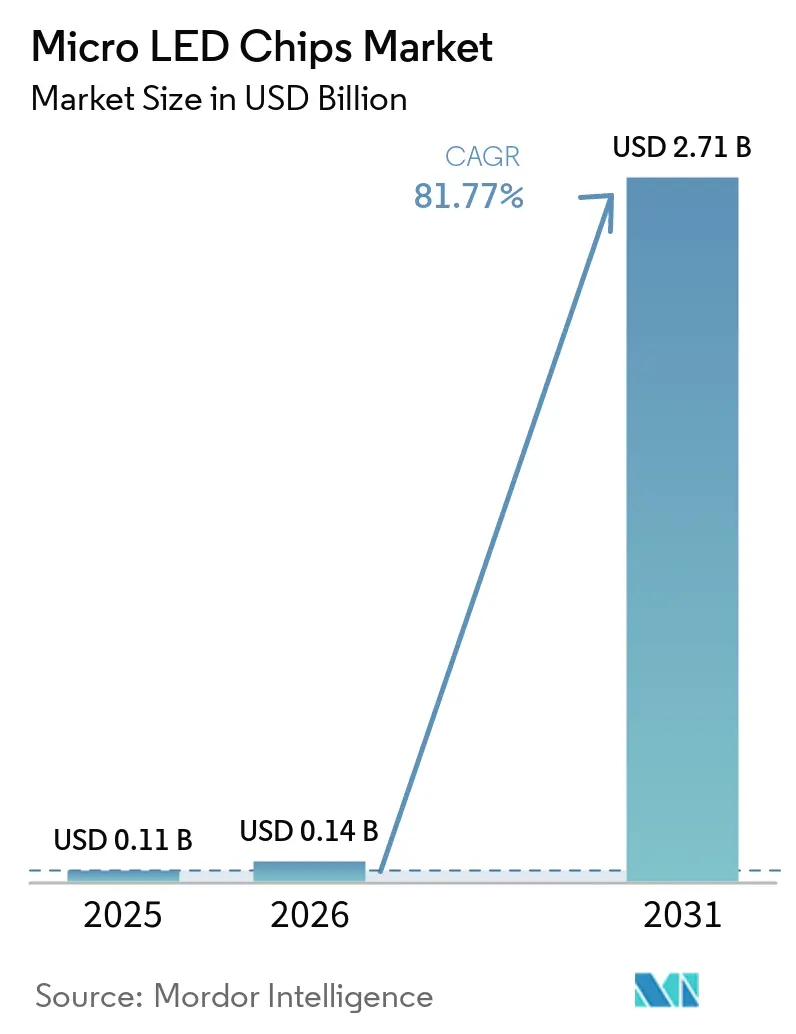
| Market Size (2026) | USD 0.14 Billion |
| Market Size (2031) | USD 2.71 Billion |
| Growth Rate (2026 - 2031) | 81.77% CAGR |
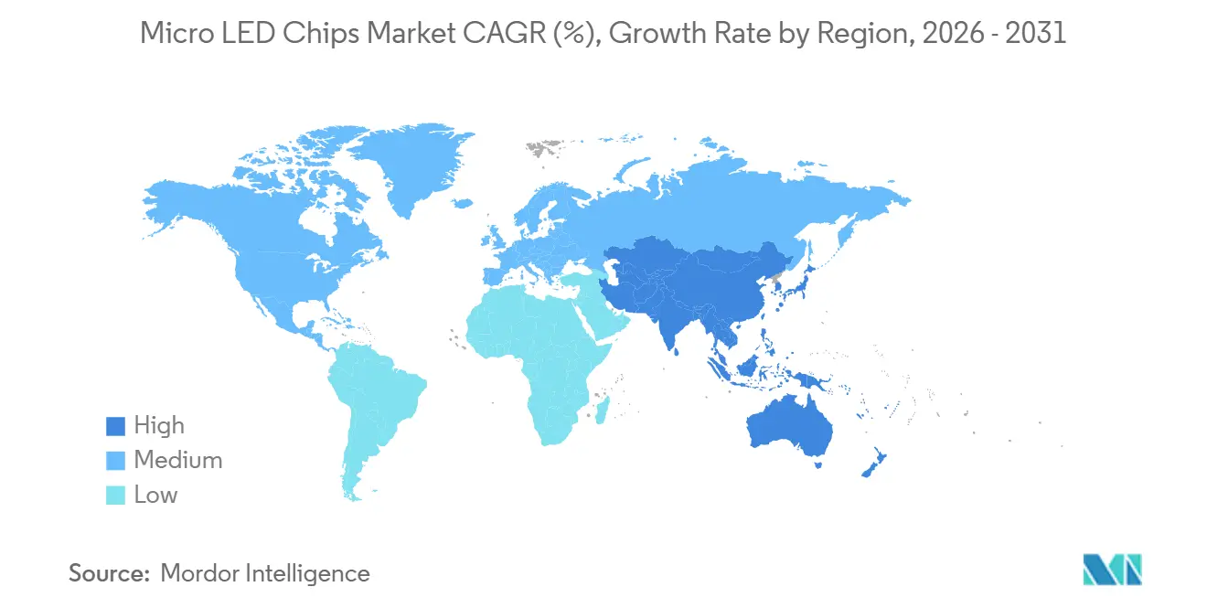
| Fastest Growing Market | Asia Pacific |
| Largest Market | Asia Pacific |
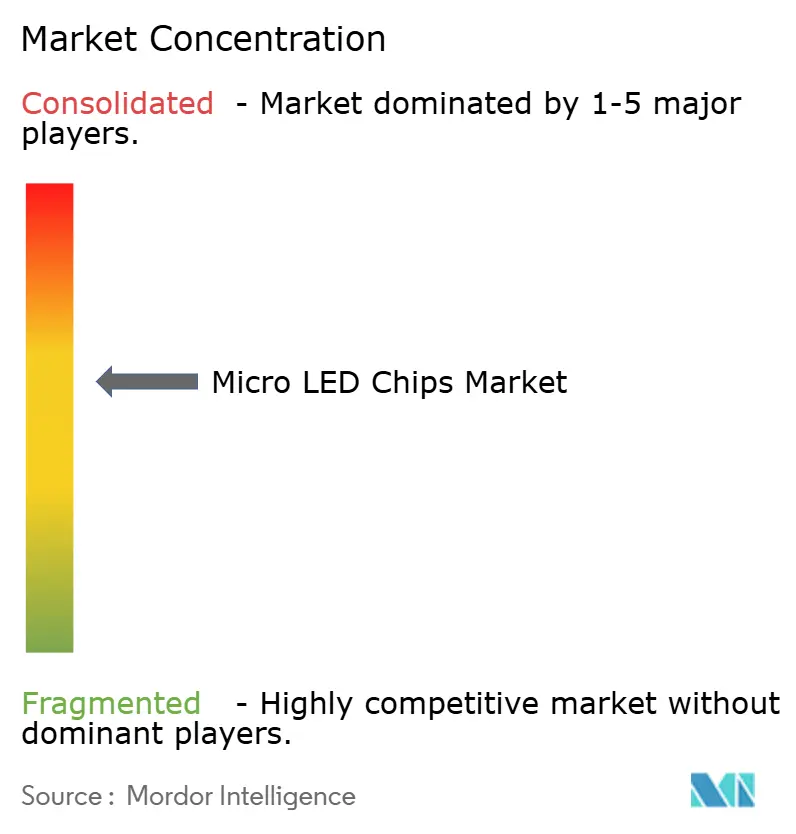
| Market Concentration | Medium |
Major Players
*Disclaimer: Major Players sorted in no particular order Image © Mordor Intelligence. Reuse requires attribution under CC BY 4.0. |
|
Micro LED Chips Market Analysis by Mordor Intelligence
The micro LED chips market size is projected to expand from USD 0.108 billion in 2025 and USD 0.137 billion in 2026 to USD 2.71 billion by 2031, registering a CAGR of 81.77% between 2026 and 2031. Six-inch GaN-on-silicon wafer adoption is cutting epitaxial costs by roughly half every two years, while laser-based mass transfer now moves more than 400 chips per second, collapsing a historic manufacturing bottleneck. Automakers seeking sunlight-readable head-up displays above 50,000 nits and television brands chasing 100% BT.2020 color gamut are accelerating volume commitments, even though red AlGaInP dies below 10 µm still post yields under 60%. Capital intensity remains formidable; new high-volume lines demand more than USD 600 million, but CHIPS-style subsidies are starting to redistribute capacity beyond East Asia. Competitive intensity is high yet fragmented; vertical integration by Samsung, LG, and BOE is catalyzing a wave of consolidation that could reshape the cost curve over the forecast horizon.
Key Report Takeaways
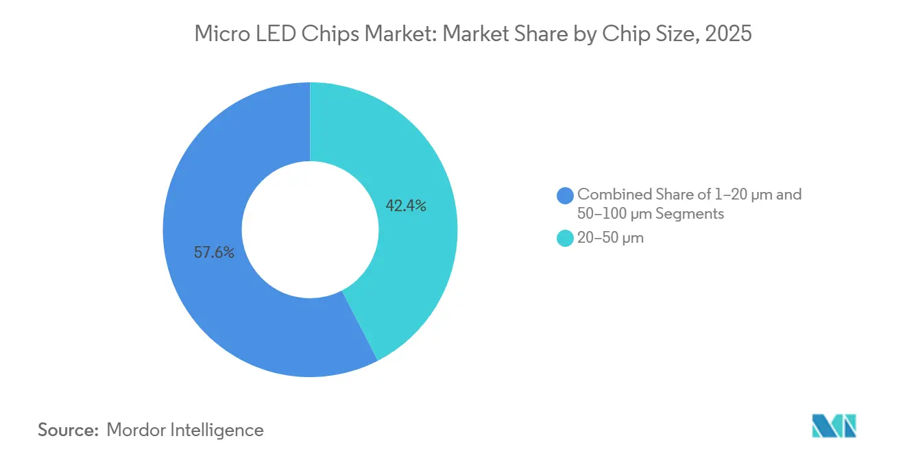
- By chip size, the 20-50 µm segment commanded 42.40% of 2025 revenue, while the 1-20 µm category is set to grow at an 83.21% CAGR on smartwatch and AR demand.
- By semiconductor material, GaN and InGaN accounted for 93.80% of shipments in 2025, yet AlGaInP is projected to climb at an 83.12% CAGR as passivation lifts external quantum efficiency to 22.3%.
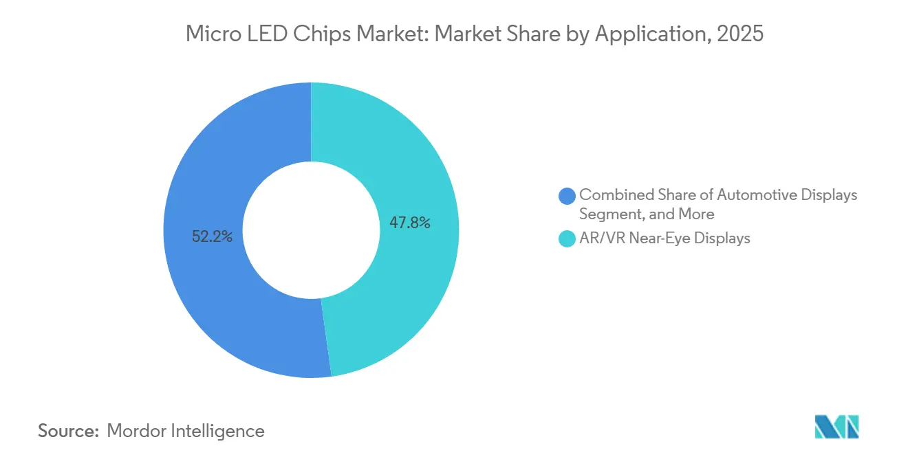
- By application, AR/VR near-eye displays captured 47.80% of 2025 revenue, but smartwatches and wearables are expected to post the fastest expansion at an 84.10% CAGR.
- By geography, the Asia Pacific led the micro LED chip market with 62.30% market share in 2025 and is forecast to grow at an 84.36% CAGR through 2031.
Note: Market size and forecast figures in this report are generated using Mordor Intelligence’s proprietary estimation framework, updated with the latest available data and insights as of January 2026.
Global Micro LED Chips Market Trends and Insights
Drivers Impact Analysis*
| DRIVER | (~) % IMPACT ON CAGR FORECAST | GEOGRAPHIC RELEVANCE | IMPACT TIMELINE |
|---|---|---|---|
| Accelerating Apple and Samsung In-house Micro LED Integration Roadmaps | +18.5% | Global, early deployment in North America and Asia Pacific | Medium term (2-4 years) |
| Cost Declines from Six-Inch GaN-on-Si Wafer Scale-Up | +16.2% | Asia Pacific core, spill-over to North America and Europe | Long term (≥ 4 years) |
| Laser-Based Mass-Transfer Throughput Gains > 400 Chips/Sec | +14.8% | Global, pilots in Taiwan, South Korea, China | Short term (≤ 2 years) |
| Automotive OEM Demand for Sun-Readable HUDs in EV Platforms | +12.3% | North America, Europe, China EV hubs | Medium term (2-4 years) |
| Government CHIPS-style Incentives for Domestic Micro-Display Fabs | +9.1% | United States, European Union, and select Asia Pacific nations | Long term (≥ 4 years) |
| Quantum-Dot Color Conversion Surpassing 80% Efficiency | +7.4% | Global, with R&D leadership in United States and Taiwan | Long term (≥ 4 years) |
| Source: Mordor Intelligence | |||
Accelerating Apple and Samsung In-house Micro LED Integration Roadmaps
CES 2026 confirmed that Samsung’s television roadmap now spans 55-130-inch Micro RGB models, achieving 100% BT.2020 color without blue-light hazard certification.[1]Samsung Electronics, “CES 2026 Micro RGB Line-up,” news.samsung.com LG countered with its Micro RGB Evo series, signaling a strategic pivot away from reliance on OLEDs and toward vertically integrated supply chains.[2]LG Display, “Micro RGB Evo Series Launch,” lgnewsroom.com Sony trademarked “True RGB” for its Crystal LED S Series, underscoring that premium brands see branding as a lever to capture early adopters. Apple remains publicly silent, but its watch prototypes suggest an exploratory posture that contrasts with Samsung’s aggressive scale-up. This divergence creates a two-speed ecosystem where television economics may subsidize die-size learning curves for wearable and AR form factors.
Cost Declines from Six-Inch GaN-on-Si Wafer Scale-Up
BOE HC Semitek’s USD 700 million Zhuhai project will deliver 58,000 six-inch wafers annually, quadrupling usable die area relative to legacy four-inch lines and slashing per-chip epitaxial cost by roughly 50%.[3]BOE Technology, “Six-Inch Wafer Expansion,” boe.com PlayNitride projects that the learning curve will push the micro LED chip market to market size parity with OLED by 2028 for high-brightness use cases. Hunan University’s six-inch GaN-on-Si wafers exceeding 10 million nits confirm optical integrity at larger diameters. A USD 1.5 billion CHIPS Act award is enabling GlobalFoundries to build a Western Hemisphere GaN-on-Si source, reducing geopolitical risk for automotive and defense applications. Together, these moves compress the cost gap with OLED and reposition supply chains geographically.
Laser-Based Mass-Transfer Throughput Gains > 400 Chips/Sec
Laser-induced forward transfer and laser lift-off now exceed 400 chips per second, shifting the primary cost driver from placement to epitaxial yield. KAIST demonstrated that hybrid laser-fluidic workflows lift placement yield by 61.8%, reducing panel cycle time from hours to minutes.[4]KAIST, “Fluidic Self-Assembly Yield Gains,” kaist.ac.kr Jade Bird Displays’ Roadrunner platform leverages this throughput to hit 10,160 PPI at 2.5 µm pitch, winning designs with Xiaomi and Meta. AUO’s automotive HUD collaboration with Sony Honda Mobility validates that laser transfer meets sub-micrometer tolerances needed for windshield projection.[5]AUO Corporation, “AFEELA 1 HUD Collaboration,” auo.com With transfer efficiency largely solved, color uniformity and red-die yield are emerging as the new bottlenecks.
Automotive OEM Demand for Sun-Readable HUDs in EV Platforms
BOE’s HERO 2.0 HUD reaches 50,000 nits, ten times brighter than LCD alternatives and fully readable under desert noon light. Peugeot’s Polygon concept and AUO’s AFEELA 1 modules highlight OEM appetite for augmented-reality guidance at premium price points. Tianma’s automotive-qualified micro LED units and VueReal’s smart mirrors extend the addressable market into exterior lighting. Certification remains a hurdle; no ISO 26262 or AEC-Q102 frameworks yet exist for micro LED HUDs, dampening volume contracts. San’an’s AEC-Q100-qualified display chip suggests that suppliers investing early in automotive validation will secure the first commercial programs.
Restraints Impact Analysis*
| RESTRAINT | (~) % IMPACT ON CAGR FORECAST | GEOGRAPHIC RELEVANCE | IMPACT TIMELINE |
|---|---|---|---|
| Yield < 60% for Sub-10 µm Red LEDs Below 4-Inch Wafers | –8.7% | Global, acute in the U.S. and Europe, four-inch fabs | Short term (≤ 2 years) |
| > USD 600 M CapEx Barrier for Greenfield High-Volume Lines | –6.4% | Global, severe for SMEs in the United States/Europe | Medium term (2-4 years) |
| Lack of Automotive Qualification Standards for Micro LED HUDs | -4.2% | North America, Europe, and China automotive corridors | Medium term (2-4 years) |
| Concentrated Supply of GaN-on-Si Wafers in East Asia | -3.1% | Global, with supply-chain risk concentrated in Taiwan, China, and South Korea | Long term (≥ 4 years) |
| Source: Mordor Intelligence | |||
Yield < 60% for Sub-10 µm Red LEDs Below 4-Inch Wafers
The external quantum efficiency of sub-10 µm AlGaInP red dies rose to 22.3% with aluminum-nitride passivation, yet commercial yields still trail those of green and blue counterparts by a wide margin. Side-wall oxidation reduces non-radiative recombination but has not lifted yields above 60%, creating scrap costs that erode margins. Samsung and LG navigate this by using larger red dies for televisions, where die counts per panel are lower. Wearable and AR devices instead deploy blue GaN arrays with quantum-dot down-conversion, adding cost and process steps. Industry consensus holds that six-inch AlGaInP wafers could reduce edge exclusion and thermal gradients, but no public yield data yet exist for that diameter.
> USD 600 M CapEx Barrier for Greenfield High-Volume Lines
BOE HC Semitek has committed to expanding its wafer operations, Jade Bird Display has invested in a new panel line, and ASE has allocated funds for a backend facility. These moves highlight that even mid-scale ventures in the industry require significant investments. The CHIPS Act has granted Intel a substantial amount, complemented by a loan, and has also allocated funds for TSMC's Arizona facility. These figures emphasize that such significant projects often hinge on government co-investment for their financial viability. As a result, smaller innovators find themselves licensing intellectual property or entering joint ventures, thereby diluting their ownership stakes. xLight's recent letter of intent for a free-electron laser suggests that the next generation of lithography could come with an even steeper price tag, potentially raising the barriers to entry. Consequently, the market landscape is increasingly favoring a select few vertically integrated giants, thereby limiting supply diversity.
*Our forecasts treat driver/restraint impacts as directional, not additive. The impact forecasts reflect baseline growth, mix effects, and variable interactions.
Segment Analysis
By Chip Size: Sub-20 µm Densities Propel Wearables and AR
The 1-20 µm segment is forecast to post an 83.21% CAGR, the fastest among all size classes, as Garmin’s USD 1,999.99 Fenix 8 Pro MicroLED proves consumer readiness to pay for 4,500-nit daylight performance. Jade Bird Display’s 10,160 PPI Roadrunner micro panel showcases that density, not die cost, defines near-eye adoption curves. However, battery life still trails AMOLED, and driver IC integration must improve to close the power gap.
Large-format displays gravitate toward 50-100 µm dies, where yields are higher, and mass-transfer tolerances are looser. Samsung’s 130-inch set and LG’s 100-inch model rely on sub-100 µm RGB LEDs to hit 100% BT.2020 color while maintaining cost discipline at wall-scale diagonals. Automotive HUD units sit between, using 20-50 µm dies to balance density with throughput; BOE’s HERO 2.0 and Tianma’s modules exemplify this sweet spot.


By Semiconductor Material: GaN Reigns, AlGaInP Rebounds
GaN and InGaN held 93.80% of 2025 shipments, bolstered by decades of LED lighting investment and a robust foundry ecosystem. Yet AlGaInP is projected to compound at 83.12% through 2031, buoyed by recent 22.3% EQE breakthroughs that restore competitiveness for deep-red emission. Quantum-dot down-conversion with an efficiency above 80% presents a stopgap but introduces thermal-aging risk for automotive cockpits. Samsung and LG’s willingness to ship true RGB televisions suggests confidence that AlGaInP yields are finally maturing for large dies.
InGaN-red remains a promising but nascent path; 12% EQE demos hint at a fully monolithic RGB future that could simplify epitaxy and improve the economics of the long-term micro LED chip market. GlobalFoundries’ GaN-on-Si line in Vermont also underwrites U.S. supply for defense and EV customers needing domestic substrates. Chinese leaders San’an and BOE hedge across both chemistries, filing 360 micro-LED patents to protect their optionality.
By Application: Wearables Outpace AR on Shipping Units
Smartwatches and wearables are forecast to expand at an 84.10% CAGR, edging past AR/VR headsets. Garmin’s Fenix 8 Pro MicroLED is the first mainstream device proving sunlight readability can command a USD 500 premium over AMOLED. AUO’s supply win confirms that Taiwan’s specialty panel makers can meet volume and quality needs.
AR glasses remain developmental; Meta and Xiaomi have design wins, but commercial launches await cost and power convergence. Television use surged after Samsung’s CES 2026 reveal and LG’s competing line, sparking a premium home-cinema battle. Automotive HUDs form a fast-follower segment as Peugeot, Sony, Honda Mobility, and Continental test prototypes. Industrial and medical displays are poised to become future adjacencies as ISO 13485 and IEC 60601 compliance paths harden.
Geography Analysis
Asia Pacific generated 62.30% of 2025 revenue and is projected to grow at an 84.36% CAGR, making it the anchor of the micro LED chips market. China’s “speed-and-scale” model is epitomized by BOE’s 58,000-wafer Zhuhai fab and San’an’s 5,000 kk-unit mini-LED ramp, giving the region unmatched die supply depth. Taiwan champions ultra-high-resolution niches; AUO’s Garmin panel win, and ASE’s USD 579 million backend plant in Kaohsiung reflect an ecosystem strategy. South Korea leads in integrated TV assembly but still imports many chips, indicating room for upstream investment.
North America’s outlook hinges on the execution of the CHIPS Act. USD 1.5 billion is funding GlobalFoundries’ GaN-on-Si line, while Intel and TSMC are collecting a combined USD 25.5 billion for advanced-node fabs that may house micro LED and driver components. A 25% tariff on imported advanced chips, effective January 2026, could nudge OEMs toward domestic sourcing but raises near-term costs. Europe lacks comparable incentives, relying on imports for epitaxy and panels, though automotive OEM interest via Peugeot indicates latent demand.
South America and the Middle East are early-stage markets where premium outdoor signage and automotive upgrades will seed adoption. Local manufacturing is absent, but micro LEDs’ longevity and brightness can justify imports for flagship retail façades and luxury EV dashboards. Regulatory gaps, especially around automotive safety standards, are global, slowing deployment even where technical readiness is proven.

Competitive Landscape
The micro LED chip market is fragmented, with a concentration in the tier. Samsung and LG leverage decades of display know-how to internalize epitaxy, transfer, and final assembly, evidenced by Samsung’s 130-inch set and LG’s Micro RGB Evo line, both shipping in 2026. BOE mirrors this vertical push in China with a USD 700 million wafer investment.
Jade Bird Display and VueReal typify fab-lite innovators targeting the AR and automotive niches through IP licensing and joint ventures. San’an’s patent portfolio and mini-LED scale-up underscore China’s ambition to dominate both GaN and AlGaInP chemistries. Strategy archetypes now cluster into three camps: (1) vertically integrated TV giants pursuing cost leadership, (2) fabless design houses monetizing IP across assemblers, and (3) niche specialists targeting high-margin wearables and HUDs.
Laser transfer throughput and quantum-dot conversion efficiency are the leading differentiation levers. U.S. subsidies for GaN-on-Si wafers threaten East Asia’s share of the substrate supply, potentially redrawing global sourcing maps once Vermont capacity comes online. Consolidation watch-points include Samsung’s rumored interest in acquiring Taiwan’s Epistar back-end assets and BOE’s overtures toward equipment vendor Kulicke & Soffa, moves that could elevate the combined top-five share.
Micro LED Chips Industry Leaders
-
Samsung Electronics Co., Ltd.
-
LG Display Co., Ltd.
-
Sony Group Corporation
-
AUO Corporation
-
BOE Technology Group Co., Ltd.
- *Disclaimer: Major Players sorted in no particular order

Recent Industry Developments
- January 2026: Samsung unveiled a 130-inch Micro RGB television using sub-100 µm LEDs with 100% BT.2020 gamut.
- January 2026: LG launched the Micro RGB Evo series with Alpha11 AI processor across 100-, 86-, and 75-inch models.
- January 2026: The U.S. imposed a 25% tariff on imported advanced chips, including micro-LED dies.
- December 2025: San’an introduced the Aimaipu brand and disclosed 5,000 kk/month mini-LED capacity plus 360 micro-LED patents.


Global Micro LED Chips Market Report Scope
The Micro LED Chips Market Report is Segmented by Chip Size (1-20 µm, 20-50 µm, and 50-100 µm), Semiconductor Material (GaN/InGaN and AlGaInP), Application (Smartwatches and Wearables, AR/VR Near-Eye Displays, Television, Smartphones and Tablets, Automotive Displays, Digital Signage/Large Displays, and Other Applications), and Geography (North America, Europe, Asia Pacific, South America, and Middle East and Africa). The Market Forecasts are Provided in Terms of Value (USD).
| 1–20 µm |
| 20–50 µm |
| 50–100 µm |
| GaN / InGaN |
| AlGaInP |
| Smartwatches & Wearables |
| AR/VR Near-Eye Displays |
| Television |
| Smartphones & Tablets |
| Automotive Displays |
| Digital Signage / Large Displays |
| Other Applications (Industrial, Medical) |
| North America |
| Europe |
| Asia Pacific |
| South America |
| Middle East and Africa |
| By Chip Size | 1–20 µm |
| 20–50 µm | |
| 50–100 µm | |
| By Semiconductor Material | GaN / InGaN |
| AlGaInP | |
| By Application | Smartwatches & Wearables |
| AR/VR Near-Eye Displays | |
| Television | |
| Smartphones & Tablets | |
| Automotive Displays | |
| Digital Signage / Large Displays | |
| Other Applications (Industrial, Medical) | |
| By Geography | North America |
| Europe | |
| Asia Pacific | |
| South America | |
| Middle East and Africa |


Key Questions Answered in the Report
How fast is revenue growing for micro-LED chips?
The micro-LED chips market size is projected to rise from USD 0.137 billion in 2026 to USD 2.71 billion by 2031, registering an 81.77% CAGR.
Which region leads demand?
Asia Pacific commanded 62.30% of 2025 revenue and is set to expand at an 84.36% CAGR through 2031, driven by aggressive Chinese and Taiwanese capacity buildouts.
What is the main technical bottleneck?
Red AlGaInP dies below 10 µm still post yields under 60%, complicating the production of full-color micro-LED displays.
Why are wearables important to adoption?
Smartwatches, led by Garmin’s Fenix 8 Pro, prove consumers will pay for 4,500-nit readability, making wearables the fastest-growing segment with an 84.10% CAGR.
How big is the capital barrier?
Building a greenfield high-volume micro-LED fab costs more than USD 600 million, limiting entry to large conglomerates or firms backed by CHIPS-style subsidies.
What advantage do micro-LEDs bring to automobiles?
Sun-readable HUDs exceeding 50,000 nits and potential exterior smart-lighting applications give micro-LEDs a brightness edge over OLED and LCD solutions.
Page last updated on:


