IoT Semiconductor Silicon Wafer Market Size and Share
Market Overview
| Study Period | 2020 - 2031 |
|---|---|
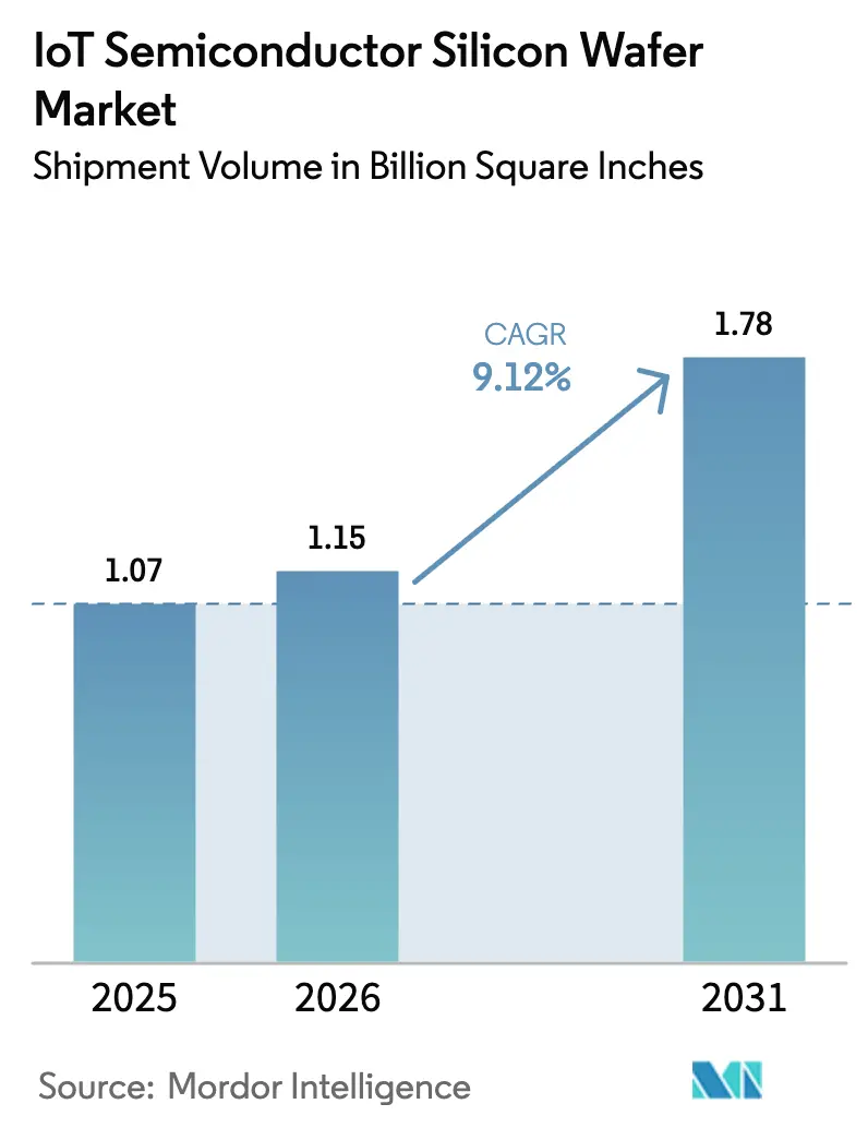
| Market Volume (2026) | 1.15 Billion Square Inches |
| Market Volume (2031) | 1.78 Billion Square Inches |
| Growth Rate (2026 - 2031) | 9.12% CAGR |
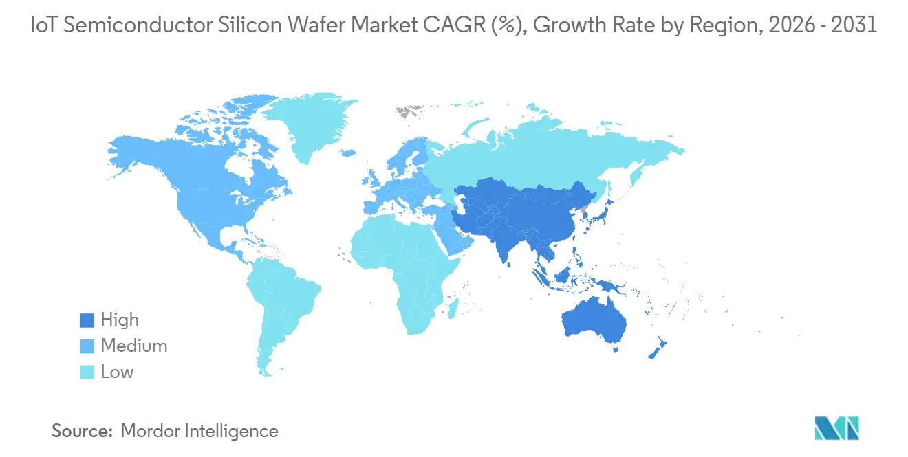
| Fastest Growing Market | Asia Pacific |
| Largest Market | Asia Pacific |
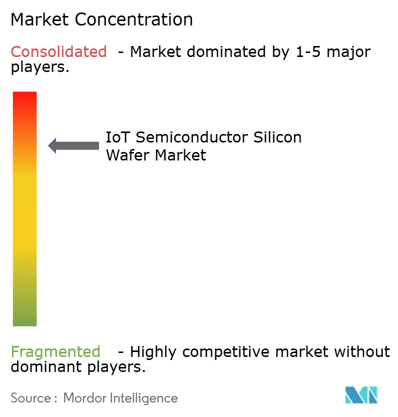
| Market Concentration | High |
Major Players *Disclaimer: Major Players sorted in no particular order Image © Mordor Intelligence. Reuse requires attribution under CC BY 4.0. | |
IoT Semiconductor Silicon Wafer Market Analysis by Mordor Intelligence
The IoT semiconductor silicon wafer market size is expected to increase from 1.07 billion square inches in 2025 to 1.15 billion square inches in 2026 and reach 1.78 billion square inches by 2031, growing at a CAGR of 9.12% over 2026-2031. A structural shift toward edge-AI inference is steering designs from legacy geometries to advanced-node processing, tightening the link between wafer demand and compute density. Policy incentives in the United States and Europe are channeling fresh capital into domestic 300 mm facilities, gradually diluting the region’s dependence on Asia-Pacific supply chains. Long-term supply pacts signed by automotive and industrial OEMs are locking in allocations at both mature and leading-edge nodes, creating a two-tier demand profile that supports high utilization across diameter classes. At the same time, polysilicon price swings and a scarcity of refurbished 200 mm tools keep cost pressure elevated, reinforcing the need for strategic inventory buffers throughout the IoT semiconductor silicon wafer market.
Key Report Takeaways
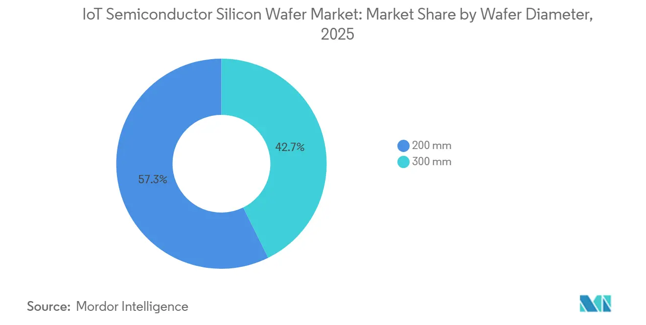
- By wafer diameter, the 200 mm category held 57.33% of the IoT semiconductor silicon wafer market share in 2025, while 300 mm substrates are projected to expand at a 10.43% CAGR through 2031.
- By technology node, mature nodes above 28 nm accounted for 64.61% of the IoT semiconductor silicon wafer market in 2025, whereas advanced node is advancing at a 10.64% CAGR through 2031.
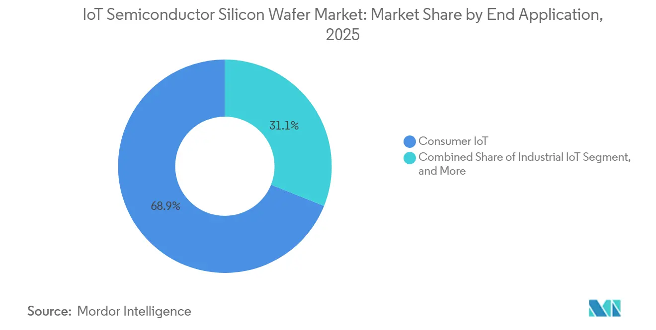
- By application, consumer IoT accounted for 68.94% of the market share in 2025; industrial IoT is forecast to post the fastest CAGR of 10.73% over 2026-2031.
- By geography, Asia-Pacific led with 69.84% of the market share in 2025 and is growing at 10.91% CAGR through 2031.
Note: Market size and forecast figures in this report are generated using Mordor Intelligence’s proprietary estimation framework, updated with the latest available data and insights as of January 2026.
Global IoT Semiconductor Silicon Wafer Market Trends and Insights
Drivers Impact Analysis*
| Driver | (~) % Impact on CAGR Forecast | Geographic Relevance | Impact Timeline |
|---|---|---|---|
| Surging 300 mm Capacity Expansion Among Foundries | +2.3% | Asia-Pacific core, spill-over to North America and Europe | Medium term (2-4 years) |
| Advanced-Node Demand From Edge-AI Enabled IoT Devices | +2.1% | Global, with concentration in Asia-Pacific and North America | Short term (≤ 2 years) |
| Government Chip Incentives CHIPS and EU Chips Acts | +1.8% | North America and Europe, indirect effects in Asia-Pacific | Long term (≥ 4 years) |
| Rising Adoption of 200 mm Wafers for Power and MEMS IoT Chips | +1.4% | Global, especially Asia-Pacific and Europe | Medium term (2-4 years) |
| Strategic Long-Term Supply Agreements With Automotive IoT OEMs | +1.2% | Europe and North America, extending to Asia-Pacific | Long term (≥ 4 years) |
| Sustainability Requirements Driving Low-Defect Wafer Processes | +0.8% | Europe and North America, gradual adoption in Asia-Pacific | Long term (≥ 4 years) |
| Source: Mordor Intelligence | |||
Surging 300 mm Capacity Expansion Among Foundries
Foundries committed more than USD 150 billion to 300 mm fabs from 2024 to early 2026, adding high-volume clean-rooms in the United States, Taiwan, South Korea, and Germany. These mega-fabs slash cost per wafer by leveraging larger die yields and higher automation levels, allowing process shrink roadmaps to proceed without eroding margins. Equipment cascades from 300 mm conversions also shrink the pool of usable 200 mm tools, fortifying pricing power for machinery brokers. Customer demand for advanced automotive and industrial logic has already filled pre-production slots, underscoring how the IoT semiconductor silicon wafer market benefits when capacity and complexity rise in tandem.[1]Taiwan Semiconductor Manufacturing Company, “TSMC Annual Report 2024,” tsmc.com
Advanced-Node Demand From Edge-AI Enabled IoT Devices
Smart cameras, predictive-maintenance modules, and medical wearables now embed neural cores that deliver inference locally, cutting latency and sidestepping privacy concerns. A flagship 4 nm processor draws under 5 W while pushing 48 TOPS, a power-performance point unattainable on 28 nm or larger nodes. As data-protection laws tighten in Europe and North America, OEMs accelerate the pivot to advanced wafers even when unit costs rise. Foundries, for their part, prioritize sub-7 nm capacity for edge-AI customers because die-yield learning curves are steeper, boosting revenue per square inch. This virtuous loop adds meaningful lift to the IoT semiconductor silicon wafer market CAGR.[2]Qualcomm, “QCS8550 IoT Processor Product Brief,” qualcomm.com
Government Chip Incentives (CHIPS and EU Chips Acts)
Federal subsidies covering 20-30% of capital outlays compress payback periods on greenfield fabs, tipping boardroom decisions in favor of domestic builds. While these projects need three-plus years to reach volume, early procurement siphons deposition and etch tools away from Asia, tightening global lead times and boosting wafer ASPs. Crucially, location-based tax breaks stipulate priority allocations for critical-infrastructure and defense IoT programs, locking in future demand at Western sites. The delayed but durable effect keeps the IoT semiconductor silicon wafer market on a steeper long-range growth path.[3]U.S. Department of Commerce, “Biden-Harris Administration Announces Preliminary Terms with TSMC Arizona,” commerce.gov
Rising Adoption of 200 mm Wafers for Power and MEMS IoT Chips
Battery-operated sensors, MEMS accelerometers, and low-voltage regulators remain sweet-spot products for 200 mm lines, where tool depreciation is complete and cycle times are short. Foundries extending these nodes to new materials such as GaN and SiC unlock higher voltage ratings without requalifying 300 mm stacks. Automotive Tier-1s now specify 200 mm supply assurance clauses in contracts, reflecting the criticality of power devices to EV drivetrains and ADAS modules. Elevated utilization above 90% shields mature nodes from price erosion, thereby sustaining a healthy slice of the IoT semiconductor silicon wafer market.
Restraints Impact Analysis*
| Restraint | (~) % Impact on CAGR Forecast | Geographic Relevance | Impact Timeline |
|---|---|---|---|
| Scarcity of Refurbished 200 mm Fab Tools | -1.2% | Global, acute in Europe and North America | Short term (≤ 2 years) |
| Geopolitical Export Controls on Advanced Nodes | -0.9% | China and Russia, indirect effects globally | Medium term (2-4 years) |
| High Capital Outlay for Below 7 nm Wafer Production | -0.7% | Global, concentrated in Asia-Pacific | Long term (≥ 4 years) |
| Volatile Polysilicon and Specialty Gas Pricing | -0.6% | Global, with Asia-Pacific most exposed | Short term (≤ 2 years) |
| Source: Mordor Intelligence | |||
Scarcity of Refurbished 200 mm Fab Tools
OEMs halted new 200 mm tool production a decade ago, so fabs extending mature nodes scavenge decommissioned lines. Broker prices for etchers and CVD gear have doubled since 2023, while requalification protocols mandated by automotive safety standards stretch lead times to two years. This equipment bottleneck caps the growth ceiling for power-management ICs and MEMS sensors despite robust end-market orders, trimming momentum in the IoT semiconductor silicon wafer market.
Geopolitical Export Controls on Advanced Nodes
Restrictions barring extreme-ultraviolet lithography shipments to China divert sub-7 nm ambitions toward Taiwan, South Korea, and the United States. Chinese foundries pivot to 14 nm and above, stifling local edge-AI chip ecosystems and shrinking prospective wafer demand. Western OEMs in turn reroute advanced designs away from Chinese fabs to avoid sanctions exposure, rearranging supply lanes but not enlarging total capacity. The real-world outcome is lost efficiency and marginally softer growth for the IoT semiconductor silicon wafer market.[4]Bureau of Industry and Security, “Advanced Computing and Semiconductor Manufacturing Items Final Rule,” bis.doc.gov
*Our forecasts treat driver/restraint impacts as directional, not additive. The impact forecasts reflect baseline growth, mix effects, and variable interactions.
Segment Analysis
By Wafer Diameter: 300 mm Gains Ground on Scaling Economics
The 200 mm segment controlled 57.33% of IoT semiconductor silicon wafer market share in 2025, illustrating the endurance of power devices and MEMS sensors that thrive on depreciated toolsets. Nevertheless, 300 mm shipments are projected to climb at a 10.43% CAGR to 2031, reflecting an economic calculus in which each larger wafer yields more than twice the dies, spreading mask and equipment costs across greater output. The IoT semiconductor silicon wafer market size tied to 300 mm nodes is therefore expanding faster than overall industry volume growth.
Asian foundries with deep balance sheets are converting 200 mm modules en masse, freeing legacy gear for resale yet amplifying scarcity in regions without similar capital incentives. European fabs continue to sweat 200 mm assets because automotive clients prize supply-chain familiarity over leading-edge density. Over time, however, power-device lines are also adopting 300 mm substrates to access longer die channels and higher current ratings, a shift that keeps the IoT semiconductor silicon wafer market in continuous evolution.


By Technology Node: Advanced Nodes Capture Edge-AI Premium
Mature nodes above 28 nm accounted for 64.61% of the IoT semiconductor silicon wafer market size in 2025, powering microcontrollers, Bluetooth radios, and analog front-ends where die cost outweighs computational heft. Advanced Node, by contrast, will log a 10.64% CAGR through 2031 as edge-AI accelerators and 5G modems demand higher transistor density per milliwatt. Foundries rolling out gate-all-around architectures report 40% lower power draw at equal performance, a metric that directly lengthens battery life in wearables and remote sensors.
Mainstream nodes from 14 nm to 22 nm bridge the gap, servicing Wi-Fi 6E, Thread, and UWB connectivity chips that prefer modest integration over bleeding-edge complexity. Export-control regimes concentrating advanced exposure in friendly jurisdictions indirectly stabilize pricing, giving buyers predictability even as absolute costs climb. The net result is a bimodal node mix in the IoT semiconductor silicon wafer market, with both cost and performance niches well defended.
By End Application: Industrial IoT Leads Growth Trajectory
Consumer devices accounted for 68.94% of the market share in 2025, but industrial IoT is set to outpace all other verticals at a 10.73% CAGR through 2031. Predictive-maintenance sensors, digital twins, and smart-grid controllers now integrate multiple dies per module, driving wafer intensity higher than in smart-home gadgets. Accordingly, the IoT semiconductor silicon wafer market size tied to factory automation is rising quickly, even though unit volumes trail consumer shipments.
Healthcare wearables and infrastructure projects add steady upside, benefiting from clearer regulatory frameworks that mandate on-device processing for privacy and latency. Automotive applications, often bundled inside industrial IoT statistics, amplify advanced-node pull because ADAS stacks merge vision, radar, and AI compute onto a single system-on-chip. This mix pushes foundries to build multi-node portfolios, ensuring the IoT semiconductor silicon wafer market serves disparate reliability and cost targets.

Geography Analysis
Asia-Pacific dominated with 69.84% of the market share in 2025 and is projected to grow at 10.91% CAGR through 2031, underpinned by Taiwanese and South Korean mega-fabs that anchor global advanced-node capacity. China’s subsidized expansions add bulk at 28 nm and above, but yield hurdles at cutting-edge geometries keep import dependence high. Japanese wafer suppliers leverage proximity and long-term contracts to maintain bargaining leverage, while India’s back-end investments create fresh downstream demand.
North America is contributing a smaller share of the volume but is receiving significant policy momentum. The CHIPS Act funds greenfield sites in Arizona and Ohio, targeting both 3 nm logic and mature-node analog, gradually rebalancing the IoT semiconductor silicon wafer market toward a 60-40 Asia-rest-of-world split by 2031. Domestic customers, especially aerospace and defense OEMs, prioritize these fabs to satisfy local-content clauses, anchoring future utilization.
Europe maintained a significant share as automotive OEMs secured local wafer supply for functional-safety reasons. Government grants accelerate Dresden and Grenoble expansions focused on 40-nm to 90-nm power devices to address EV and industrial control demand. While no European site has committed to sub-5 nm production, collaborative ventures aim to import masks and photoresist know-how, ensuring the region retains relevance within the global IoT semiconductor silicon wafer market.

Competitive Landscape
The market is concentrated, with players such as Shin-Etsu Chemical, SUMCO, GlobalWafers, Siltronic, SK Siltron, and others supplying wafers. Foundries, by contrast, remain fragmented, with over twenty operators vying across nodes from 180 nm down to 2 nm. This structure funnels margins to the substrate tier when capacity is tight, as seen in 2024-2025 price hikes that outpaced silicon-feedstock inflation.
Vertical integration is becoming a strategic approach in the industry. Samsung’s internal wafer division provides its foundry arm with protection against spot shortages. Meanwhile, pure-play companies like TSMC rely on multi-year contracts but must accommodate price-adjustment clauses. Niche players such as Soitec and Wolfspeed are gaining market share in silicon-on-insulator and silicon-carbide substrates, leveraging technical barriers that discourage generalist competitors.
Technology competition centers on defect density and edge-exclusion metrics. Patent filings for low-oxygen crystal-growth or advanced slurry chemistries shave micro-defect counts, lifting die yields by single-digit percentages that translate into millions in annual savings at advanced nodes. Meanwhile, Intel’s entry into the external foundry arena injects a well-capitalized challenger, even if early utilization lags. Overall, bargaining power tilts toward customers at mature nodes yet swings back to suppliers at sub-7 nm, maintaining a dynamic equilibrium within the IoT semiconductor silicon wafer market.
IoT Semiconductor Silicon Wafer Industry Leaders
Shin-Etsu Chemical Co. Ltd.
SUMCO Corporation
GlobalWafers Co. Ltd.
Siltronic AG
SK Siltron Co. Ltd.
- *Disclaimer: Major Players sorted in no particular order

Recent Industry Developments
- February 2026: TSMC began volume production at Arizona Fab 21 Phase 2, adding 20,000 3 nm wafer starts per month dedicated to edge-AI processors.
- January 2026: Intel allocated USD 3.5 billion to convert two Oregon fabs from 200 mm to 300 mm, targeting analog and mature-node IoT chips.
- December 2025: National Silicon Industry Group inaugurated a 300 mm wafer plant in Zhejiang, China, with initial capacity of 200,000 wafers monthly.
- November 2025: GlobalWafers and STMicroelectronics signed a 10-year deal for 150,000 silicon-on-insulator wafers annually for RF and power IoT devices.


Global IoT Semiconductor Silicon Wafer Market Report Scope
The IoT Semiconductor Silicon Wafer Market refers to the market for silicon wafers used to produce semiconductors that enable Internet of Things (IoT) applications. These wafers serve as the foundational material for manufacturing integrated circuits, which are essential to IoT devices across industries such as consumer electronics, industrial automation, healthcare, and smart city infrastructure.
The IoT Semiconductor Silicon Wafer Market Report is Segmented by Wafer Diameter (300 mm, and 200 mm), Technology Node (Advanced Node, Mainstream Node, and Mature Node), End Application (Consumer IoT, Industrial IoT, Healthcare IoT, and Infrastructure/Smart City IoT), and Geography (North America, Europe, Asia-Pacific, South America, and Middle East and Africa). The Market Forecasts are Provided in Terms of Shipment Volume (Square Inches).
| 300 mm |
| 200 mm |
| Advanced Node (Below 7nm) |
| Mainstream Node (10nm-28nm) |
| Mature Node (Above 28nm) |
| Consumer IoT |
| Industrial IoT |
| Healthcare IoT |
| Infrastructure / Smart City IoT |
| North America | United States |
| Canada | |
| Mexico | |
| Europe | Germany |
| United Kingdom | |
| France | |
| Rest of Europe | |
| Asia-Pacific | China |
| Japan | |
| India | |
| South Korea | |
| Taiwan | |
| Rest of Asia-Pacific | |
| South America | |
| Middle East and Africa |
| By Wafer Diameter | 300 mm | |
| 200 mm | ||
| By Technology Node | Advanced Node (Below 7nm) | |
| Mainstream Node (10nm-28nm) | ||
| Mature Node (Above 28nm) | ||
| By End Application | Consumer IoT | |
| Industrial IoT | ||
| Healthcare IoT | ||
| Infrastructure / Smart City IoT | ||
| By Geography | North America | United States |
| Canada | ||
| Mexico | ||
| Europe | Germany | |
| United Kingdom | ||
| France | ||
| Rest of Europe | ||
| Asia-Pacific | China | |
| Japan | ||
| India | ||
| South Korea | ||
| Taiwan | ||
| Rest of Asia-Pacific | ||
| South America | ||
| Middle East and Africa | ||


Key Questions Answered in the Report
What is the projected IoT semiconductor silicon wafer market size by 2031?
The market is expected to reach 1.78 billion square inches by 2031.
What CAGR is projected for IoT semiconductor silicon wafers during 2026-2031?
The market is forecast to rise at a 9.12% CAGR over the 2026-2031 period.
Which wafer diameter segment shows the fastest growth?
The 300 mm category leads with a 10.43% CAGR through 2031, driven by edge-AI and 5G designs that need advanced nodes.
Which region currently supplies the majority of IoT wafers?
Asia-Pacific accounts for 69.84% of the market share in 2025 and remains the primary manufacturing hub through 2031.
How do CHIPS and EU Chips Act incentives influence capacity build-outs?
Subsidies covering 20-30% of capital costs accelerate construction of new 300 mm fabs in the United States and Europe, rebalancing global supply.
Why is refurbished 200 mm equipment in short supply?
Original equipment makers stopped producing new 200 mm tools a decade ago, so fabs rely on limited refurbished units, stretching lead times to as long as two years.
Page last updated on:


