
High-Speed PCB Market Size and Share
Market Overview
| Study Period | 2020 - 2031 |
|---|---|
| Market Size (2026) | USD 5.08 Billion |
| Market Size (2031) | USD 11.27 Billion |
| Growth Rate (2026 - 2031) | 17.28 % |
| Fastest Growing Market | North America |
| Largest Market | Asia-Pacific |
| Market Concentration | Medium |
Major Players *Disclaimer: Major Players sorted in no particular order Image © Mordor Intelligence. Reuse requires attribution under CC BY 4.0. | |
High-Speed PCB Market Analysis by Mordor Intelligence
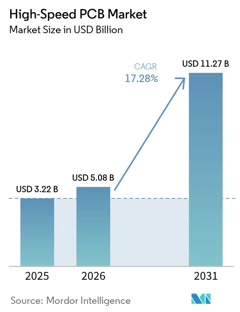
The high-speed PCB market size is expected to increase from USD 3.22 billion in 2025 to USD 5.08 billion in 2026 and to USD 11.27 billion by 2031, growing at a CAGR of 17.28% over 2026-2031. Robust capital outlays by hyperscale operators, the migration from legacy FR-4 to low-loss laminates, and the rise of 112-gigabit-per-second signaling jointly accelerate revenue growth. Cloud providers view board-level interconnect as a source of a competitive latency advantage, so they now co-design substrates with fabricators rather than buying catalog parts. Investments in substrate-like boards, glass-core technology, and sequential lamination lines mark a structural shift in value capture away from commoditized four- and six-layer products toward ultra-HDI architectures. Supply chains remain tight because only a handful of resin and copper-foil suppliers meet the electrical and thermal requirements of AI workloads, keeping pricing power in the hands of material vendors and tier-one fabricators.
Key Report Takeaways
- By PCB type, multilayer boards with 12 or more layers accounted for 38% of 2025 revenue, whereas substrate-like PCBs are forecast to grow at a 18.28% CAGR through 2031.
- By data-rate capability, 56-112 Gbps boards captured 41% of 2025 demand, and the 112 Gbps-plus segment is advancing at an 18.18% CAGR during 2026-2031 in the high-speed printed circuit board market.
- By material, low-loss laminates accounted for 46% of 2025 sales, with ultra-low-loss substrates poised to grow at an 18.07% CAGR over the same period.
- By end use, hyperscale AI data centers accounted for 59% of 2025 revenue, while cloud service providers are the fastest-growing customer group, with a 18.32% CAGR to 2031.
- By geography, Asia-Pacific led with 68% revenue share in 2025, while North America is projected to expand at an 18.38% CAGR through 2031.
Note: Market size and forecast figures in this report are generated using Mordor Intelligence’s proprietary estimation framework, updated with the latest available data and insights as of January 2026.
Market Trends and Insights
Drivers Impact Analysis of High-Speed PCB Market*
| Driver | (~) % Impact on CAGR Forecast | Geographic Relevance | Impact Timeline |
|---|---|---|---|
| Growing Demand for AI and ML GPU Clusters | +5.2% | Global, concentrated in North America and Asia-Pacific | Medium term (2-4 years) |
| Rapid Adoption of 56-112 Gbps SerDes | +4.1% | Global, led by North America and Europe | Short term (≤ 2 years) |
| Increasing Layer Counts and HDI Adoption | +2.9% | Asia-Pacific core, spillover to North America | Medium term (2-4 years) |
| Expansion of Hyperscale Capacity | +2.6% | Global, North America and Asia-Pacific leading | Long term (≥ 4 years) |
| Transition to Chiplet Architectures | +1.8% | North America and Asia-Pacific | Long term (≥ 4 years) |
| Emergence of Glass-Core Substrates | +1.2% | North America, Europe, and Japan | Long term (≥ 4 years) |
| Source: Mordor Intelligence | |||
Growing Demand for AI and ML GPU Clusters
Generative AI racks introduced in 2025 integrate more than 70 GPUs and drive aggregate interconnect bandwidth above 1 terabit per second, pushing PCB current limits past 1,800 amperes while retaining 112 Gbps signal integrity. Hyperscalers absorb the three-to-four-fold cost premium over general-purpose server boards because every microsecond of latency directly affects revenue from large-language-model queries. Capital budgets support long-term supply agreements, so fabricators that master via-in-pad HDI techniques secure multi-year volume commitments. The design complexity also increases non-recurring engineering fees, which raise average selling prices and expand the high-speed PCB market profit pool.
Rapid Adoption of 56-112 Gbps SerDes and PCIe 6.0
The PCIe 6.0 rollout in 2025 doubles per-lane bandwidth but shrinks voltage margins, making trace losses that were minor at PCIe 4.0 now mission-critical. Server boards built on ultra-low-loss epoxy or PTFE laminates with dissipation factors below 0.002 are now required to sustain a 36 decibel signal-to-noise threshold set by CPU vendors. Only four laminate suppliers worldwide can meet this standard, so supply concentration extends lead times and hardens pricing. Design houses increasingly rely on 3-D electromagnetic simulation to optimize stub length and back-drilling, elevating engineering tool spend per project.
Increasing Layer Counts and HDI Adoption
Dual-socket AI motherboards already exceed 20 layers, and some accelerator mezzanines reach 28 layers to fit dense power-delivery networks.[1] Higher layer counts are reduced via stubs, yet strain yields because stacked microvias under 150 microns require sub-25-micron laser-drilling accuracy. As a result, yield gaps of 12-15 percentage points emerge between HDI and conventional multilayer runs, raising unit costs and also creating barriers to entry for lower-tier shops. Fabricators that invested early in sequential lamination now command price premiums and gain preferred-supplier status for complex AI builds.
Expansion of Hyperscale Data Center Capacity
Operators added over 120 gigawatts of IT load in 2025, and each megawatt of AI compute needs 40-50 high-speed PCB market server boards, nearly twice the count required for virtualization stacks. Liquid cooling in AI clusters demands materials that resist dielectric fluids, so board design cycles extend and qualification tests multiply. Hyperscalers increasingly lock in dedicated production lines, insulating leading fabricators from consumer-electronics cycles, while mid-tier shops contend with volatile demand and margin compression.
Restraints Impact Analysis of High-Speed PCB Market*
| Restraint | (~) % Impact on CAGR Forecast | Geographic Relevance | Impact Timeline |
|---|---|---|---|
| Thermal Management Challenges | -1.8% | Global, acute in high-density AI clusters | Short term (≤ 2 years) |
| Supply Chain Disruptions and Lead Times | -1.5% | Global, Asia-Pacific and North America affected | Medium term (2-4 years) |
| Yield Losses in Ultra-Low-Loss Laminate | -1.1% | Asia-Pacific core, spillover to Europe | Medium term (2-4 years) |
| Export Controls on Advanced Equipment | -0.9% | Asia-Pacific, especially China | Long term (≥ 4 years) |
| Source: Mordor Intelligence | |||
Thermal Management Challenges at Ultra-High Data Rates
SerDes channels operating at 112 Gbps dissipate more than 5 watts per lane, so a 16-lane device concentrates 80 watts over less than 10 cm², driving board temperatures close to the glass-transition limit. Intel estimates that board-level cooling solutions now consume up to 22% of module costs. Immersion cooling alters dielectric constants, shifting impedance by up to 12 ohms, which forces trace-geometry compensation and raises design complexity. Resulting field-return rates for AI servers run 40% higher than traditional systems, inflating warranty reserves.
Supply Chain Disruptions and Material Lead Times
Lead times for ultra-low-loss laminates have significantly increased to 20 weeks following a fire at a resin plant in 2025, which eliminated a critical portion of production capacity. Rogers Corporation has confirmed that its capacity is fully booked through mid-2026, forcing server OEMs to adopt dual-sourcing strategies for boards and to increase their safety-stock coverage to 8-12 weeks. Additionally, export controls on advanced drilling tools have further constrained the expansion of Chinese HDI manufacturing capabilities.[2] This situation has redirected excess demand to alternative markets such as Taiwan and Vietnam, where higher freight and tariff costs are exerting additional pressure on profit margins.
*Our forecasts treat driver/restraint impacts as directional, not additive. The impact forecasts reflect baseline growth, mix effects, and variable interactions.
High-Speed PCB Market Segment Analysis
By PCB Type:
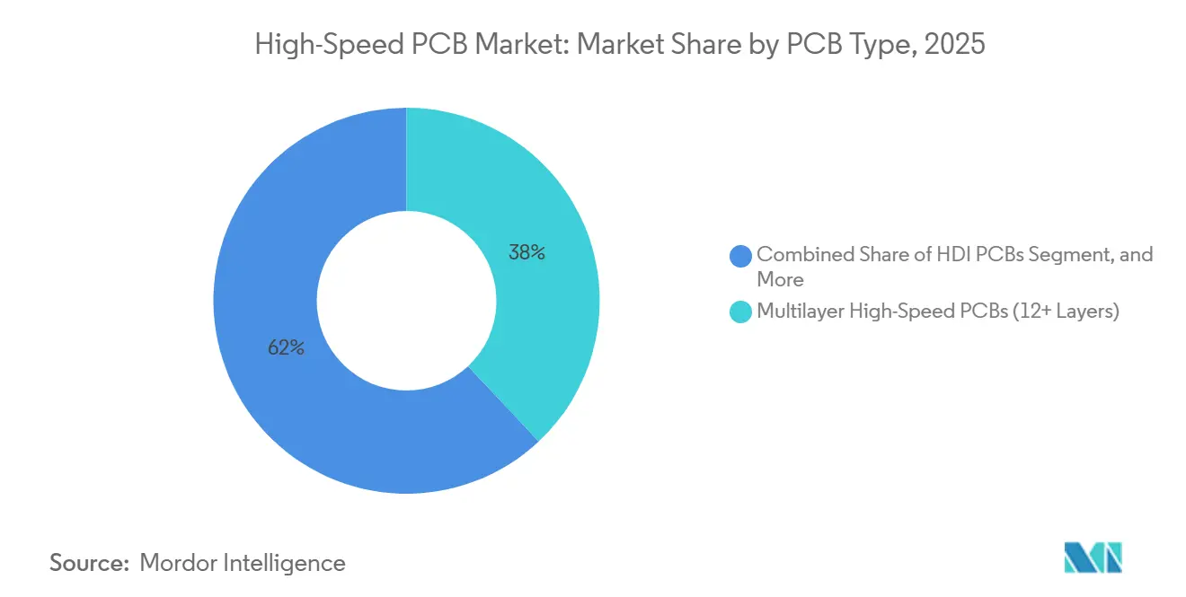
Substrate-Like Designs Move Center StageMultilayer boards with 12 or more layers accounted for 38% of revenue in 2025, underscoring their role as the workhorse platform for dual-socket servers. These boards account for the largest slice of the high-speed PCB market share because they balance density, cost, and manufacturability for 56 Gbps workloads. Substrate-like PCBs, however, are climbing at an 18.28% CAGR as chiplet architectures propagate across accelerator roadmaps. The high-speed PCB market for these substrate-like formats will grow as AMD, Intel, and NVIDIA bring organic interposers priced at USD 150-200 per module into production.
Substrate-like boards demand line-and-space below 10 microns and via densities over 10,000 vias/mm², positioning them halfway between advanced packaging and traditional PCB realms. Fabricators such as AT&S and Ibiden channel more than USD 500 million each into new Malaysian and Japanese lines to address this demand. HDI boards retain relevance in edge servers where space is scarce, while backplanes continue to dominate storage fabrics that prize low-crosstalk over micro-via density. This mixed technology stack favors diversified suppliers rather than single-niche shops.

By Data Rate Capability:
112 Gbps-Plus Boards Lead GrowthBoards engineered for 56-112 Gbps links secured 41% of 2025 revenue, powered by PCIe 5.0 and 100G Ethernet deployments. Even so, the 112 Gbps-plus cohort is projected to rise at an 18.18% CAGR, making it the fastest contributor to overall high-speed PCB market growth. High-speed printed circuit board market size gains in this category reflect PCIe 6.0 motherboards and 800G switch line cards that require insertion losses below 30 decibels across 30-inch traces.
Meeting these budgets obliges designers to shorten via stubs below 5 mils, adopt controlled-impedance routing tolerances of ±3%, and shift to PTFE or hydrocarbon-based laminates. Capital needs escalate because a single 67 gigahertz vector network analyzer now costs USD 300,000, yet without such metrology, fabricators cannot win hyperscale qualifications. Lower-speed boards up to 25 Gbps remain prevalent in edge compute and small-office networking, but revenue gradually gravitates toward the higher data-rate tiers as AI inference proliferates.
By Material Type:
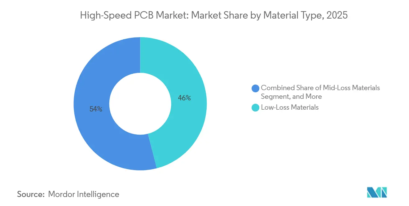
Ultra-Low-Loss Laminates AccelerateLow-loss epoxy laminates accounted for 46% of 2025 revenue because they offer a pragmatic balance between electrical performance and ease of fabrication. However, ultra-low-loss materials with dissipation factors below 0.002 will expand fastest at an 18.07% CAGR through 2031, driven by 112 Gbps boards in AI accelerators. Switching to these substrates lowers equalization overhead in SerDes receivers by 40%, saving die area while preserving signal margins above 36 dB. Consequently, hyperscalers accept board costs four to five times higher than FR-4 to unlock system-level power savings.
Standard FR-4 remains the cost-effective choice for cost-sensitive edge appliances, while mid-loss variants serve PCIe 4.0 systems that fall between the extremes. Material vendors thus segment their portfolios and pricing tiers, capturing additional value as performance thresholds ratchet higher. The high-speed PCB market benefits because fabricators integrating ultra-low-loss stacks can justify premium pricing and book longer-term contracts insulated from commodity swings.
By End-Use Industry:
AI Clusters Dominate DemandHyperscale AI data centers absorbed 59% of 2025 demand, cementing their status as the revenue anchor for high-speed PCB market participants. The GB200 and DGX H100 platforms each deploy dozens of 112 Gbps differential pairs per board, elongating design cycles but also lifting average selling prices. Cloud service providers, meanwhile, register an 18.32% CAGR as they retrofit brownfield facilities and build sovereign clouds that keep sensitive models on-shore.
Enterprise HPC and government research maintain stable though smaller volumes, typically adopting designs proven first at hyperscale. Procurement patterns thus form a two-speed cycle, leading fabricators chase early-adopter AI programs, while mid-tier shops service enterprise migrations 12-24 months later. Niche military or satellite contracts further diversify revenue for specialists qualified to IPC-6012 Class 3, but unit counts pale in comparison to hyperscale rollouts.
Geography Analysis
APAC High-Speed PCB Market
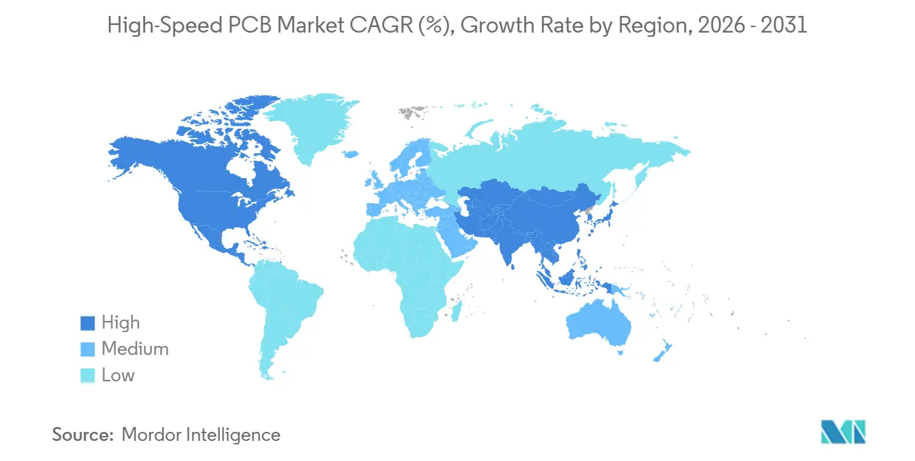
Asia-Pacific accounted for 68% of 2025 sales, driven by the robust manufacturing capabilities of Taiwan, China, Japan, and South Korea. These countries host extensive capacities across drilling, plating, and assembly processes, consolidated within highly integrated campuses. The region's vendors benefit significantly from economies of scale and their strategic proximity to laminate and copper-foil production facilities. This proximity ensures the high-speed PCB market remains cost-competitive, particularly for mainstream AI server applications. Additionally, the presence of co-located research and development centers fosters rapid process innovation and iteration, providing the region with a critical time-to-market advantage in a highly competitive global market.
North America High-Speed PCB Market
North America, though smaller in volume, is the fastest-growing region, with a 18.38% CAGR through 2031, driven by sovereign-compute mandates requiring domestic assembly for national-security workloads. Programs such as the CHIPS and Science Act steer subsidies toward PCB and semiconductor facilities, so fabricators like TTM Technologies earmark USD 150 million for ultra-HDI expansion in New York.[3] This reshoring partially offsets supply-chain risk and shortens lead times for U.S. defense and cloud operators, enlarging the regional high-speed PCB market share.
EMEA and South America High-Speed PCB Market
Europe keeps a high-mix, high-complexity focus. Austria-based AT&S and Germany-based sites invest in substrate-like and glass-core boards that command premium pricing, though absolute volumes remain modest compared with Asia. South America, the Middle East, and Africa remain niche, supplying telecom and industrial boards rather than AI servers. Overall, a bifurcated geography emerges, with volume tilting toward Asia while value and resilience tilt toward North America and select European plants.
Competitive Landscape
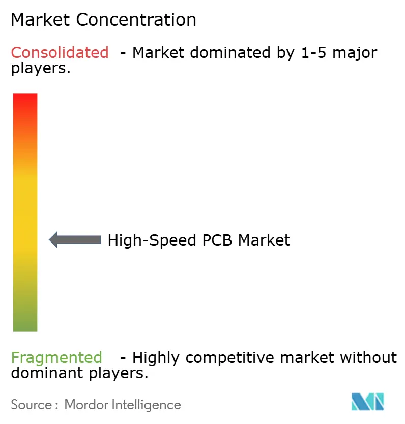
The ten largest suppliers captured approximately 55-60% of the 2025 revenue, reflecting a moderately consolidated market structure. Taiwanese giants, such as Unimicron and Nan Ya PCB, operate at a significant scale, with each running twelve or more HDI (High-Density Interconnect) production lines capable of processing 50,000 m² monthly. This level of operational capacity creates substantial barriers to entry for new greenfield players. Meanwhile, South Korean and Japanese vendors maintain their competitive edge in high-layer-count niches by leveraging advanced technologies, including laser drilling capabilities below 75 microns and expertise in sequential lamination processes. These specialized capabilities enable them to serve demanding applications, further solidifying their market position.
Strategic differentiation now hinges on embedding optical waveguides, mastering glass-core substrates, and offering impedance assurance within ±3% in-line. Samsung Electro-Mechanics invested KRW 1.8 trillion (USD 1.35 billion) in Vietnam to co-locate laminate casting with assembly, shrinking cycle times for hyperscale bids. AT&S and Ibiden each committed more than USD 500 million to pilot glass-substrate lines after Intel validated the technology, betting that chiplet designs will spill from silicon interposers to organic panels.[4]
Nimble North American and European shops leverage two-week quick-turn production models tailored for AI startups, enabling them to command significant price premiums despite lacking the massive production capacity of larger competitors. This operational agility serves as a strategic hedge against potential export-control shocks, which could disrupt the import of critical tooling and equipment from the Asia-Pacific region. Over the forecast period, competitive intensity is expected to remain high as fabricators aggressively compete to secure hyperscale design wins. These design wins not only provide long-term demand visibility but also generate the necessary revenue streams to fund subsequent rounds of capital expenditure, ensuring sustained growth and innovation in the market.
High-Speed PCB Industry Leaders
-
TTM Technologies Inc.
-
Unimicron Technology Corp.
-
Ibiden Co., Ltd.
-
Samsung Electro-Mechanics Co., Ltd.
-
AT&S Austria Technologies and Systemtechnik AG
- *Disclaimer: Major Players sorted in no particular order
High-Speed PCB Market Companies Covered in this Report
- TTM Technologies Inc.
- Unimicron Technology Corp.
- Ibiden Co., Ltd.
- Samsung Electro-Mechanics Co., Ltd.
- AT&S Austria Technologie and Systemtechnik AG
- Compeq Manufacturing Co., Ltd.
- Nan Ya Printed Circuit Board Corp.
- Shennan Circuits Co., Ltd.
- Zhen Ding Technology Holding Limited
- Tripod Technology Corp.
- CMK Corporation
- Meiko Electronics Co., Ltd.
- WUS Printed Circuit Co., Ltd.
- Chin-Poon Industrial Co., Ltd.
- Sanmina Corporation
- Flex Ltd. (Multek)
- Kyocera Corporation
- RayMing Technology
- Advanced Circuits Inc.
- Shenzhen Kinwong Electronic Co., Ltd.
Recent Industry Developments in High-Speed PCB Market
- April 2025: Meiko Electronics earned IPC-6012 Class 3 certification for a 28-layer ultra-HDI line in Japan.
- March 2025: Samsung Electro-Mechanics completed phase one of its KRW 1.8 trillion (USD 1.35 billion) Vietnam HDI plant, adding 20-layer capacity for AI server boards.
- March 2025: Nan Ya PCB and Rogers Corporation began co-developing laminates with dissipation factors below 0.0015.
- February 2025: AT&S allocated EUR 500 million (USD 565 million) to a Malaysian site dedicated to substrate-like PCBs with line-and-space below 10 µm.
Global High-Speed PCB Market Report Scope
The High-Speed PCB market refers to the global industry that designs, manufactures, and supplies printed circuit boards engineered to support high-frequency, high-data-rate signal transmission with minimal loss, distortion, and electromagnetic interference. These PCBs are critical for enabling reliable performance in advanced computing and communication systems, particularly in environments requiring data rates exceeding 25 Gbps and scaling beyond 112 Gbps.
The High Speed PCB Market Report is Segmented by PCB Type (Multilayer High-Speed PCBs 12+ Layers, HDI PCBs, Ultra-Low-Loss/High-Frequency PCBs, Backplane PCBs, and Substrate-Like PCBs), Data Rate Capability (Up to 25 Gbps, 25-56 Gbps, 56-112 Gbps, and 112 Gbps+), Material Type (Standard FR-4, Mid-Loss Materials, Low-Loss Materials, and Ultra-Low-Loss Materials), End-Use Industry (Hyperscale Data Centers AI/ML Clusters, Cloud Service Providers, Enterprise HPC, and Government/Research Labs), and Geography (North America, South America, Europe, Asia-Pacific, and Middle East, Africa). The Market Forecasts are Provided in Terms of Value (USD).
Segmentation Overview
| Multilayer High-Speed PCBs (12+ Layers) |
| HDI PCBs |
| Ultra-Low-Loss / High-Frequency PCBs |
| Backplane PCBs |
| Substrate-Like PCBs |
| Up to 25 Gbps |
| 25-56 Gbps |
| 56-112 Gbps |
| 112 Gbps+ |
| Standard FR-4 |
| Mid-Loss Materials |
| Low-Loss Materials |
| Ultra-Low-Loss Materials |
| Hyperscale Data Centers (AI/ML Clusters) |
| Cloud Service Providers |
| Enterprise HPC |
| Government / Research Labs |
| North America | United States | |
| Canada | ||
| Mexico | ||
| South America | Brazil | |
| Argentina | ||
| Rest of South America | ||
| Europe | United Kingdom | |
| Germany | ||
| France | ||
| Italy | ||
| Rest of Europe | ||
| Asia-Pacific | China | |
| Japan | ||
| India | ||
| South Korea | ||
| Rest of Asia-Pacific | ||
| Middle East and Africa | Middle East | United Arab Emirates |
| Saudi Arabia | ||
| Rest of Middle East | ||
| Africa | South Africa | |
| Egypt | ||
| Rest of Africa | ||
| By Sensor Type | Multilayer High-Speed PCBs (12+ Layers) | ||
| HDI PCBs | |||
| Ultra-Low-Loss / High-Frequency PCBs | |||
| Backplane PCBs | |||
| Substrate-Like PCBs | |||
| By Data Rate Capability | Up to 25 Gbps | ||
| 25-56 Gbps | |||
| 56-112 Gbps | |||
| 112 Gbps+ | |||
| By Material Type | Standard FR-4 | ||
| Mid-Loss Materials | |||
| Low-Loss Materials | |||
| Ultra-Low-Loss Materials | |||
| By End-User Industry | Hyperscale Data Centers (AI/ML Clusters) | ||
| Cloud Service Providers | |||
| Enterprise HPC | |||
| Government / Research Labs | |||
| By Geography | North America | United States | |
| Canada | |||
| Mexico | |||
| South America | Brazil | ||
| Argentina | |||
| Rest of South America | |||
| Europe | United Kingdom | ||
| Germany | |||
| France | |||
| Italy | |||
| Rest of Europe | |||
| Asia-Pacific | China | ||
| Japan | |||
| India | |||
| South Korea | |||
| Rest of Asia-Pacific | |||
| Middle East and Africa | Middle East | United Arab Emirates | |
| Saudi Arabia | |||
| Rest of Middle East | |||
| Africa | South Africa | ||
| Egypt | |||
| Rest of Africa | |||
Key Questions Answered in the Report
What is the 2025 High speed PCB market size and how fast is it expected to grow?
The High speed PCB market size reached USD 5.08 billion in 2026 and is forecast to rise to USD 11.27 billion by 2031 at a 17.28% CAGR.
Which geographic region is expanding fastest in High speed PCB deployments?
North America shows the quickest expansion with an anticipated 18.38% CAGR through 2031 as sovereign-compute mandates stimulate domestic AI infrastructure builds.
Why are ultra-low-loss laminates gaining popularity in server boards?
Ultra-low-loss substrates enable insertion-loss budgets under 1 dB-per-inch, which is essential for 112 Gbps signaling; this performance benefit justifies their higher cost for hyperscale AI clusters.
How are substrate-like PCBs reshaping supplier strategies?
Substrate-like boards blur the line between packaging and PCB fabrication, so vendors investing in line-and-space below 10 microns secure early design wins in chiplet-based accelerators.
What thermal challenges arise at 112 Gbps data rates?
SerDes lanes dissipate more than 5 watts each, concentrating 80 watts in small board areas, which forces adoption of vapor chambers, liquid cooling, and tighter impedance control to avoid signal degradation.
How consolidated is the High speed PCB supplier landscape?
The top ten fabricators account for roughly 55-60% of global revenue, signaling moderate consolidation driven by scale, HDI expertise, and supply-chain control rather than outright monopoly.