High-Resistivity Silicon Wafer Market Size and Share
Market Overview
| Study Period | 2020 - 2031 |
|---|---|
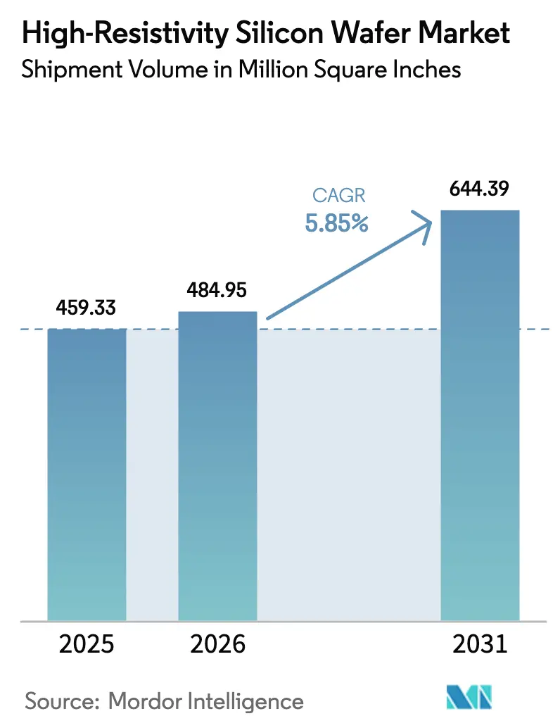
| Market Volume (2026) | 484.95 Million Square Inches |
| Market Volume (2031) | 644.39 Million Square Inches |
| Growth Rate (2026 - 2031) | 5.85% CAGR |
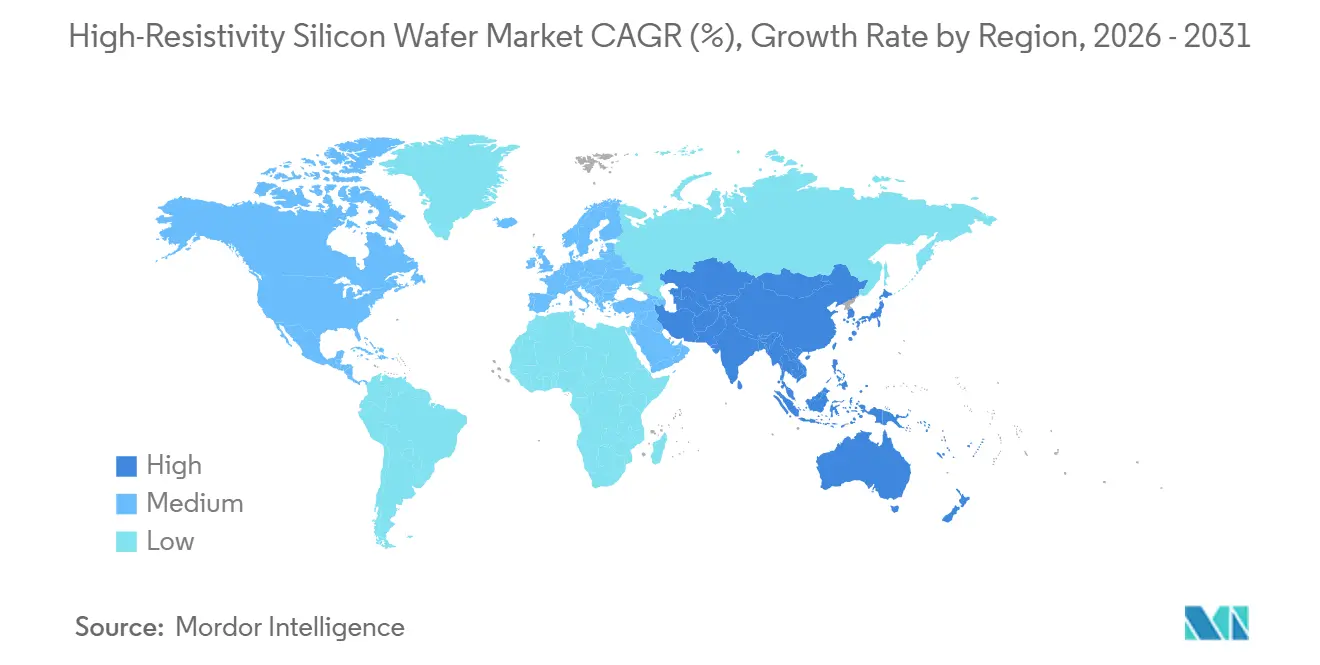
| Fastest Growing Market | Asia Pacific |
| Largest Market | Asia Pacific |
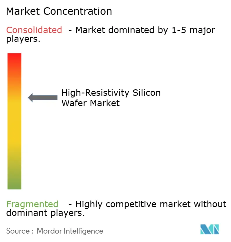
| Market Concentration | Medium |
Major Players *Disclaimer: Major Players sorted in no particular order Image © Mordor Intelligence. Reuse requires attribution under CC BY 4.0. | |
High-Resistivity Silicon Wafer Market Analysis by Mordor Intelligence
The high-resistivity silicon wafer market size is expected to increase from 459.33 million square inches in 2025 to 484.95 million square inches in 2026 and reach 644.39 million square inches by 2031, growing at a CAGR of 5.85% over 2026-2031. Operators rolling out 5G macro and small-cell sites have locked in multi-year purchases of RF-SOI switches and power amplifiers, guaranteeing baseline demand even as handset unit growth slows. Radar content per car is rising because Level 2+ assistance features are becoming mandatory in Europe and China, and each additional sensor requires substrates with resistivity above 1,000 ohm-cm. Photonic integrated-circuit vendors are now qualifying 300 mm high-resistivity platforms, shifting the wafer mix toward larger diameters. Finally, government incentives in the United States, Europe, and Japan are accelerating domestic capacity additions, cushioning buyers against geopolitical supply shocks.
Key Report Takeaways
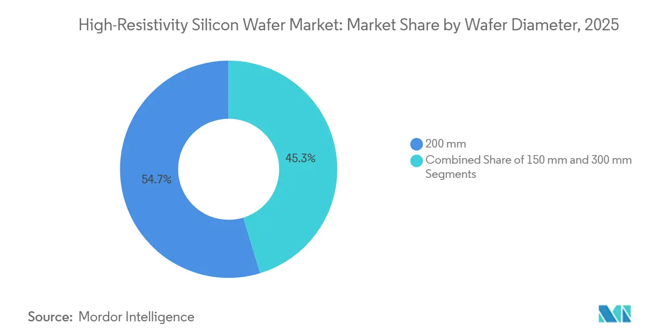
- By wafer diameter, the 200 mm format commanded 54.68% of the high-resistivity silicon wafer market share in 2025, while the 300 mm format is projected to expand at a 6.74% CAGR through 2031.
- By wafer type, polished high-resistivity silicon accounted for 38.86% of the high-resistivity silicon wafer market size in 2025, and HR-SOI substrates is advancing at a 6.48% CAGR over 2026-2031.
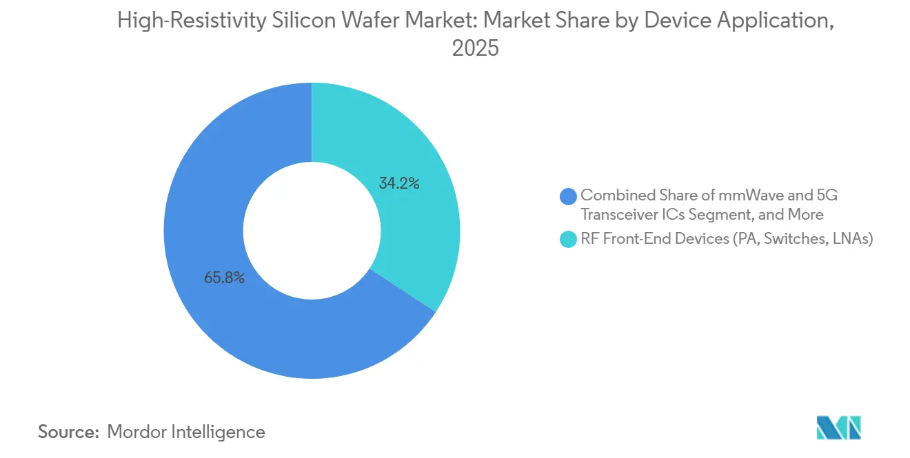
- By device application, RF front-end components led with 34.24% of the high-resistivity silicon wafer market share in 2025; mmWave and 5 G transceiver ICs is forecasted to grow at a 6.83% CAGR through 2031.
- By end-user, telecommunications accounted for 32.73% of the high-resistivity silicon wafer market in 2025, whereas automotive demand is set to grow at a 6.26% CAGR during 2026-2031.
- By geography, Asia-Pacific captured 58.89% of the high-resistivity silicon wafer market in 2025, and will register the fastest regional growth at 6.98% CAGR to 2031.
Note: Market size and forecast figures in this report are generated using Mordor Intelligence’s proprietary estimation framework, updated with the latest available data and insights as of January 2026.
Global High-Resistivity Silicon Wafer Market Trends and Insights
Drivers Impact Analysis*
| Driver | (~) % Impact on CAGR Forecast | Geographic Relevance | Impact Timeline |
|---|---|---|---|
| Growing Adoption of RF SOI in 5G Smartphones | +1.5% | Global, core demand in Asia-Pacific and North America | Short term (≤ 2 years) |
| Expansion of Automotive Radar Production | +0.9% | Europe and North America, accelerating in China | Medium term (2-4 years) |
| Rising Demand for mmWave Silicon for Satellite Communications | +0.7% | North America and Europe, emerging in Asia-Pacific | Medium term (2-4 years) |
| Integration of Adaptive Beamforming in Phased-Array Antennas | +0.6% | Global, clustered in defense and telecom hubs | Long term (≥ 4 years) |
| Development of Photonic ICs on High-Resistivity Substrates | +0.5% | North America and Europe, pilot lines in Asia-Pacific | Long term (≥ 4 years) |
| Government Incentives for On-shore Semiconductor Manufacturing | +0.3% | United States, Europe, Japan, India | Medium term (2-4 years) |
| Source: Mordor Intelligence | |||
Growing Adoption of RF SOI in 5G Smartphones
Every 5G handset now ships with RF-SOI front-end circuitry, cementing a structural pull on the high-resistivity silicon wafer market.[1]Soitec, “RF-SOI Technology for 5G Applications,” SOITEC.COM The trap-rich layer in HR-SOI limits substrate coupling above 2 GHz, letting power amplifiers meet linearity targets without external filters. Component value per phone climbed from USD 1.20 in 2020 to USD 2.10 in 2024, and designers have already reserved 200 mm capacity through 2027. As sub-6 GHz coverage broadens across India, South-East Asia, and South America, wafer demand remains resilient despite plateauing handset units.
Expansion of Automotive Radar Production
The European Union’s 2024 safety regulation mandates multiple 77-81 GHz radars per new vehicle, elevating high-resistivity wafer consumption in Europe and North America.[2]European Commission, “General Safety Regulation for Motor Vehicles,” EC.EUROPA.EU Silicon-based radar on HR-SOI delivers 15% lower phase noise than bulk CMOS at 77 GHz, supporting advanced driver-assistance functions.[3]IEEE, “28 nm FD-SOI CMOS for 77 GHz Automotive Radar Applications,” IEEEXPLORE.IEEE.ORG As China’s NCAP tightens in 2025, domestic brands are adding corner and rear radar, driving double-digit substrate growth through the decade.
Rising Demand for mmWave Silicon for Satellite Communications
Low-Earth-orbit constellations deploy user terminals that integrate Ka-band phased arrays fabricated on high-resistivity silicon, with each unit consuming roughly 400 mm² of wafer area. DARPA’s 2025 G-band program channels USD 150 million into silicon-based 140 GHz transceivers, aiming to cut device cost below USD 500. As deployments scale, annual wafer pull could rival handset RF demand by 2029, broadening the high-resistivity silicon wafer industry customer base.
Integration of Adaptive Beamforming in Phased-Array Antennas
3GPP Release 18 requires beam updates every 0.5 ms, forcing RF and digital blocks onto the same die where low-loss substrates are essential.[4]3GPP, “Release 18 Specifications for Enhanced Beamforming,” 3GPP.ORG Qualcomm’s X80 modem integrates a 16-element array on HR-SOI, shrinking module footprint by 30% and setting a benchmark for mid-band 5G hardware. Defense radar programs mirror this trend, elevating long-term demand for high-resistivity silicon wafer market products.
Restraints Impact Analysis*
| Restraint | (~) % Impact on CAGR Forecast | Geographic Relevance | Impact Timeline |
|---|---|---|---|
| Complexities in Producing Defect-Free 300 mm HR Wafers | -0.8% | Global, acute in new North American and European fabs | Short term (≤ 2 years) |
| Price Premium over Conventional Silicon Wafers | -0.4% | Global, most pronounced in cost-sensitive consumer devices | Medium term (2-4 years) |
| Supply Constraints of Ultra-High-Purity Float-Zone Silicon | -0.6% | Japan and Germany dominated supply chain | Short term (≤ 2 years) |
| Emerging GaN and SiC Substrates for RF and Power Devices | -0.5% | North America and Europe lead adoption | Long term (≥ 4 years) |
| Source: Mordor Intelligence | |||
Complexities in Producing Defect-Free 300 mm HR Wafers
Float-zone crystal growth at 300 mm demands stringent thermal control, and initial yields trail 200 mm equivalents by up to 20 percentage points. Epitaxial uniformity within ±2 nm across a 300 mm HR-SOI wafer remains challenging, slowing customer qualifications. The USD 800 million–USD 1.2 billion price tag for a greenfield line deters new entrants, keeping supply tight and inflating spot prices until processes mature.
Price Premium over Conventional Silicon Wafers
A 200 mm polished high-resistivity wafer costs roughly USD 120-150 versus USD 40-50 for standard silicon, while HR-SOI variants reach USD 300. Consumer IoT and entry-level smartphones often sacrifice marginal RF performance to avoid this premium. Although automotive and defense applications can absorb higher substrate costs, tier-1 suppliers still push for 10-15% annual price reductions, compressing vendor margins.
*Our forecasts treat driver/restraint impacts as directional, not additive. The impact forecasts reflect baseline growth, mix effects, and variable interactions.
Segment Analysis
By Wafer Diameter: Transition Momentum Builds for 300 mm Platforms
The 200 mm segment held 54.68% of the high-resistivity silicon wafer market share in 2025, reflecting the installed base of RF-IC fabs built during the 2010s. Leading front-end vendors such as Qorvo and Skyworks continue to run mature 200 mm lines because die sizes for switches and low-noise amplifiers remain small. However, 300 mm fabs promise lower cost per die once yields stabilize, and early adopters saw an 85% yield by late 2025, narrowing the gap with 200 mm processes. Capital costs near USD 1 billion per facility slow the migration, yet the convergence of RF, baseband, and AI accelerators on a single die makes the larger format economically compelling.
Looking forward, the 300 mm segment is expected to grow at a 6.74% rate, gradually eroding the dominance of 200 mm in the high-resistivity silicon wafer market. Automotive radar ICs integrating digital signal processing will be among the first movers because rising channel counts drive die area beyond 120 mm². While 150 mm substrates linger in legacy military programs, their absolute volumes are shrinking. As yield learning improves and subsidy-backed capacity ramps in Texas, Freiberg, and Gumi, 300 mm economics will turn decisively favorable for high-volume RF devices.


By Wafer Type: HR-SOI Outpaces Polished and Epitaxial Substrates
Polished high-resistivity silicon captured 38.86% of the market share in 2025, thanks to imaging sensors and industrial detectors that value low dark current over RF isolation. Epitaxial wafers support power devices and MEMS, where a lightly doped epi-layer offers voltage blocking or mechanical benefits. HR-SOI, however, is forecast to rise at a 6.48% CAGR as 5G, Wi-Fi 7, and phased-array radars demand enhanced linearity. The RFeSI-3 platform reduced harmonic distortion by 2 dB, making HR-SOI indispensable for 26 dBm power amplifiers.
Adoption accelerates as GlobalFoundries, TSMC, and other foundries qualify HR-SOI at 300 mm, effectively doubling usable die per wafer and shrinking cost penalties. The high-resistivity silicon wafer market size for HR-SOI substrates is therefore set to expand more quickly than the total market volume. Supply concentration remains a double-edged sword: Soitec’s 60% share offers stable quality but exposes the ecosystem to single-point failures, prompting tier-1 IC houses to dual-source from Shin-Etsu and SUMCO where possible.
By Device Application: mmWave Transceivers Become the Next Anchor Segment
RF front-end parts accounted for 34.24% of the market share in 2025, but commoditization pressures vendors to cut the cost per switch or amplifier every year. mmWave and 5G transceiver ICs, by contrast, are growing at 6.83% as satellite broadband and fixed-wireless-access rollouts multiply. Each Ka-band user terminal needs roughly 400 mm² of high-resistivity silicon, a sizable pull on wafer capacity. Automotive radar chips also migrate toward larger, more integrated dies, supporting robust demand.
The high-resistivity silicon wafer market size tied to mmWave devices could eclipse that of legacy RF switches by 2029. Defense and aerospace applications add further upside because phased-array radars and electronic-warfare modules increasingly favor silicon over gallium-arsenide for cost reasons. Imaging and photonic ICs continue as stable specialty niches, procuring ultra-high-resistivity float-zone substrates despite their premium price.
By End-user: Automotive Grows Fastest as Sensor Attach Rates Rise
Telecommunications retained 32.73% share in 2025 as carriers installed 5G macro cells worldwide. That segment is leveling off in mature markets, shifting incremental growth toward India and South-East Asia. Automotive demand, however, is projected to climb at 6.26%, reflecting regulatory mandates that push radar sensor counts from three in 2025 to as many as six per vehicle by 2028. Each additional sensor maps to more RF die and thus more wafer starts, driving sustained volume growth.
Industrial and scientific end-users consume high-resistivity silicon for precision sensors operating in harsh conditions or extreme temperatures. Although smaller in absolute terms, these buyers pay price premiums that smooth revenue for suppliers. Defense and medical imaging remain small but strategic, providing stable off-cycle demand that insulates the high-resistivity silicon wafer industry from consumer electronics volatility.
Geography Analysis
Asia-Pacific dominated the high-resistivity silicon wafer market with 58.89% market share in 2025, and is projected to grow at 6.98% through 2031. Japan’s Shin-Etsu and SUMCO jointly supply half the world’s float-zone capacity, while Taiwan’s fabless RF community converts those substrates into power amplifiers exported globally. China is investing aggressively to localize float-zone production, reducing import dependence and offering wafers 20-30% cheaper than Japanese equivalents. South Korea’s SK Siltron is ramping 300 mm qualification to serve automotive radar suppliers seeking geographic diversity.
North America is adding capacity faster than historical trends because the CHIPS Act covers up to 40% of capital expenditures for specialty wafer plants. GlobalWafers broke ground in Texas with USD 400 million in federal grants, and first wafers are slated for 2027. These new lines will prioritize 300 mm HR-SOI for domestic RF-IC and automotive markets, shortening lead times and mitigating trade risks. Europe follows a similar path; Siltronic’s Freiberg expansion, backed by EUR 300 million (USD 325 million) in subsidies, positions the region to support its automotive radar ecosystem without relying solely on imports.
South America and the Middle East and Africa remain nascent consumers, but policy initiatives could unlock incremental demand. Brazil’s initial 5G rollout is importing RF front-ends that incorporate high-resistivity silicon, while the United Arab Emirates is studying a greenfield fab that would include specialty wafer capability. African uptake is negligible today, yet South Africa’s automotive sector is narrowing technology gaps that will eventually require radar ICs and, by extension, HR substrates. Although these regions contribute minimally before 2031, they represent diversification options in the next decade.

Competitive Landscape
The high-resistivity silicon wafer market shows moderate concentration, with the top five suppliers holding roughly 70% combined share in 2025. Shin-Etsu and SUMCO dominate ultrahigh-resistivity float-zone silicon, leveraging decades of process refinement to deliver defect densities suitable for 77-81 GHz RF and scientific imaging. Soitec maintains a near-monopoly on HR-SOI through its Smart Cut bonding technology, achieving gross margins above 35% and commanding premium pricing.
Capacity expansion remains the primary competitive lever. GlobalWafers’ Texas investment and Siltronic’s Freiberg project illustrate how subsidies tilt the playing field toward early movers in new geographies. Mid-tier contenders such as Okmetic and Wafer Works win share by offering smaller lot sizes and faster qualification, addressing gaps that large incumbents cannot serve efficiently. Chinese entrants, buoyed by state funding, price wafers 15-20% below Japanese benchmarks, intensifying price pressure for mainstream RF applications.
Technology differentiation now concentrates on trap-rich layer engineering that extends HR-SOI performance into upper-mmWave bands. Patent filings in 2024-2025 reveal ongoing competition to co-optimize buried-oxide thickness and trap density, delivering 1-2 dB incremental improvements in third-order intercept point. Buyers also demand closed-loop wafer reclaim services and tighter particulate specifications, forcing suppliers to invest continuously in polishing and metrology assets. Overall, strategic positioning blends geographic diversification, process innovation, and deep customer co-development programs that lock in multi-year supply contracts.
High-Resistivity Silicon Wafer Industry Leaders
Shin-Etsu Handotai Co., Ltd.
SUMCO Corporation
Siltronic AG
GlobalWafers Co., Ltd.
Soitec S.A.
- *Disclaimer: Major Players sorted in no particular order

Recent Industry Developments
- February 2026: Soitec unveiled a EUR 500 million (USD 540 million) expansion in Bernin, France, adding 300 mm HR-SOI capacity for automotive radar and 5G infrastructure. Completion is slated for Q4 2027.
- January 2026: GlobalWafers received a USD 400 million CHIPS Act grant to build a 300 mm wafer fab in Sherman, Texas, with HR-SOI production targeted for late 2027.
- December 2025: Shin-Etsu Handotai completed a JPY 120 billion (USD 850 million) upgrade at its Isobe facility, bringing new 300 mm float-zone lines on stream.
- November 2025: SUMCO and Toyota agreed to co-develop 300 mm high-resistivity wafers for next-gen 77 GHz imaging radar, under a USD 50 million joint program.


Global High-Resistivity Silicon Wafer Market Report Scope
High-Resistivity (HR) Silicon Wafers are silicon substrates with resistivity typically ≥1,000 Ω·cm, designed for applications requiring high electrical isolation and minimal signal interference. These wafers are widely used in advanced electronic devices and systems.
The High-Resistivity Silicon Wafer Market Report is Segmented by Wafer Diameter (150 mm, 200 mm, and 300 mm), Wafer Type (Polished, Epitaxial, and HR-SOI), Device Application (RF Front-End Devices, mmWave and 5G Transceiver ICs, Automotive Radar ICs, Photodetectors and Imaging Devices, and MEMS and Advanced Sensor ICs), End-user (Consumer Electronics, Industrial, Telecommunications, Automotive, and Other End-user Applications), and Geography (North America, Europe, Asia-Pacific, South America, and Middle East and Africa). The Market Forecasts are Provided in Terms of Volume (Square Inches).
| 150 mm |
| 200 mm |
| 300 mm |
| Polished High-Resistivity Silicon |
| Epitaxial High-Resistivity Silicon |
| High-Resistivity Silicon-on-Insulator (HR-SOI) |
| RF Front-End Devices (PA, Switches, LNAs) |
| mmWave and 5G Transceiver ICs |
| Automotive Radar ICs (77-81 GHz) |
| Photodetectors and Imaging Devices |
| MEMS and Advanced Sensor ICs |
| Consumer Electronics |
| Industrial |
| Telecommunications |
| Automotive |
| Other End-user Applications |
| North America | United States |
| Canada | |
| Mexico | |
| Europe | Germany |
| United Kingdom | |
| France | |
| Rest of Europe | |
| Asia-Pacific | China |
| Japan | |
| India | |
| South Korea | |
| Rest of Asia-Pacific | |
| South America | |
| Middle East and Africa |
| By Wafer Diameter | 150 mm | |
| 200 mm | ||
| 300 mm | ||
| By Wafer Type | Polished High-Resistivity Silicon | |
| Epitaxial High-Resistivity Silicon | ||
| High-Resistivity Silicon-on-Insulator (HR-SOI) | ||
| By Device Application | RF Front-End Devices (PA, Switches, LNAs) | |
| mmWave and 5G Transceiver ICs | ||
| Automotive Radar ICs (77-81 GHz) | ||
| Photodetectors and Imaging Devices | ||
| MEMS and Advanced Sensor ICs | ||
| By End-user | Consumer Electronics | |
| Industrial | ||
| Telecommunications | ||
| Automotive | ||
| Other End-user Applications | ||
| By Geography | North America | United States |
| Canada | ||
| Mexico | ||
| Europe | Germany | |
| United Kingdom | ||
| France | ||
| Rest of Europe | ||
| Asia-Pacific | China | |
| Japan | ||
| India | ||
| South Korea | ||
| Rest of Asia-Pacific | ||
| South America | ||
| Middle East and Africa | ||


Key Questions Answered in the Report
What is the projected volume for high-resistivity wafers by 2031?
It is forecast to reach 644.39 million square inches by 2031, rising at a 5.85% CAGR from 2026.
Which wafer diameter is growing the fastest?
The 300 mm format is advancing at 6.74% a year as integrated RF-digital designs migrate to larger substrates.
Why are automotive radar systems boosting wafer demand?
New safety rules mandate more 77-81 GHz sensors per vehicle, and each sensor uses high-resistivity silicon ICs that require premium substrates.
Who are the leading suppliers of high-resistivity wafers?
Shin-Etsu Handotai, SUMCO, Siltronic, GlobalWafers, and Soitec together hold roughly 70% share of global capacity.
How are government subsidies shaping supply?
Programs in the United States, Europe, and Japan underwrite up to 40% of fab costs, accelerating new 300 mm lines and diversifying geographic supply.
What threatens high-resistivity silicon’s dominance in RF?
Falling costs for gallium-nitride and silicon-carbide substrates could win designs above 28 GHz if wafer prices drop below USD 150 for a 6-inch equivalent by 2028.
Page last updated on:


