
HBM Wafer-on-Wafer (WoW) Hybrid Bonding Market Size and Share
Market Overview
| Study Period | 2020 - 2031 |
|---|---|
| Market Size (2026) | USD 0.51 Billion |
| Market Size (2031) | USD 2.06 Billion |
| Growth Rate (2026 - 2031) | 32.21 % |
| Fastest Growing Market | North America |
| Largest Market | Asia-Pacific |
| Market Concentration | Medium |
Major Players *Disclaimer: Major Players sorted in no particular order Image © Mordor Intelligence. Reuse requires attribution under CC BY 4.0. | |
HBM Wafer-on-Wafer (WoW) Hybrid Bonding Market Analysis by Mordor Intelligence
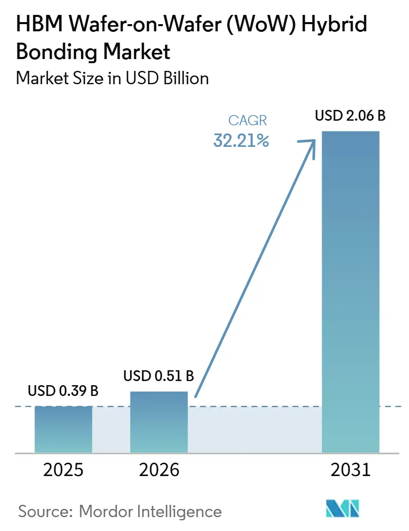
The HBM Wafer-on-Wafer (wow) hybrid bonding market size stood at USD 0.39 billion in 2025 and is forecast to reach USD 2.06 billion by 2031, growing at a CAGR of 32.21% over 2026-2031. Demand is rising because AI accelerator programs need much denser vertical interconnects than conventional micro-bump packaging can support. Roadmaps from TSMC, Samsung, and SK hynix are pushing the technology toward finer pitches, higher layer counts, and broader use in logic and memory integration, keeping equipment demand tied to multiple product generations. The transition to sub-10 micron pitch is also shifting purchasing toward bonders, metrology tools, cleaning systems, and surface preparation platforms that can support tighter process windows. Asia-Pacific remains the manufacturing center because memory production, foundry capacity, and equipment development are concentrated there, while North America is gaining momentum through domestic advanced packaging investment. Growth will remain strong, but adoption will continue to favor customers that can absorb high tool costs, long qualification cycles, and difficult yield-control requirements.
Key Report Takeaways
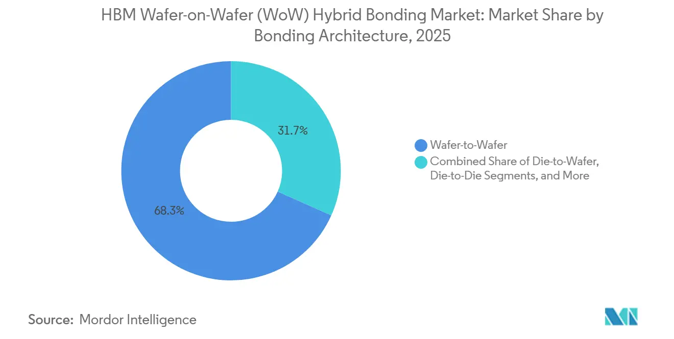
- By bonding architecture, wafer-to-wafer held 68.32% share of the HBM Wafer-on-Wafer (WoW) hybrid bonding market in 2025, while die-to-wafer is projected to expand at a 32.68% CAGR through 2031.
- By bonding type, Copper-to-Copper bonding captured 55.06% share in 2025, while Oxide-to-Oxide and Metal-Oxide Hybrid Bonding are projected to grow at a 32.61% CAGR through 2031.
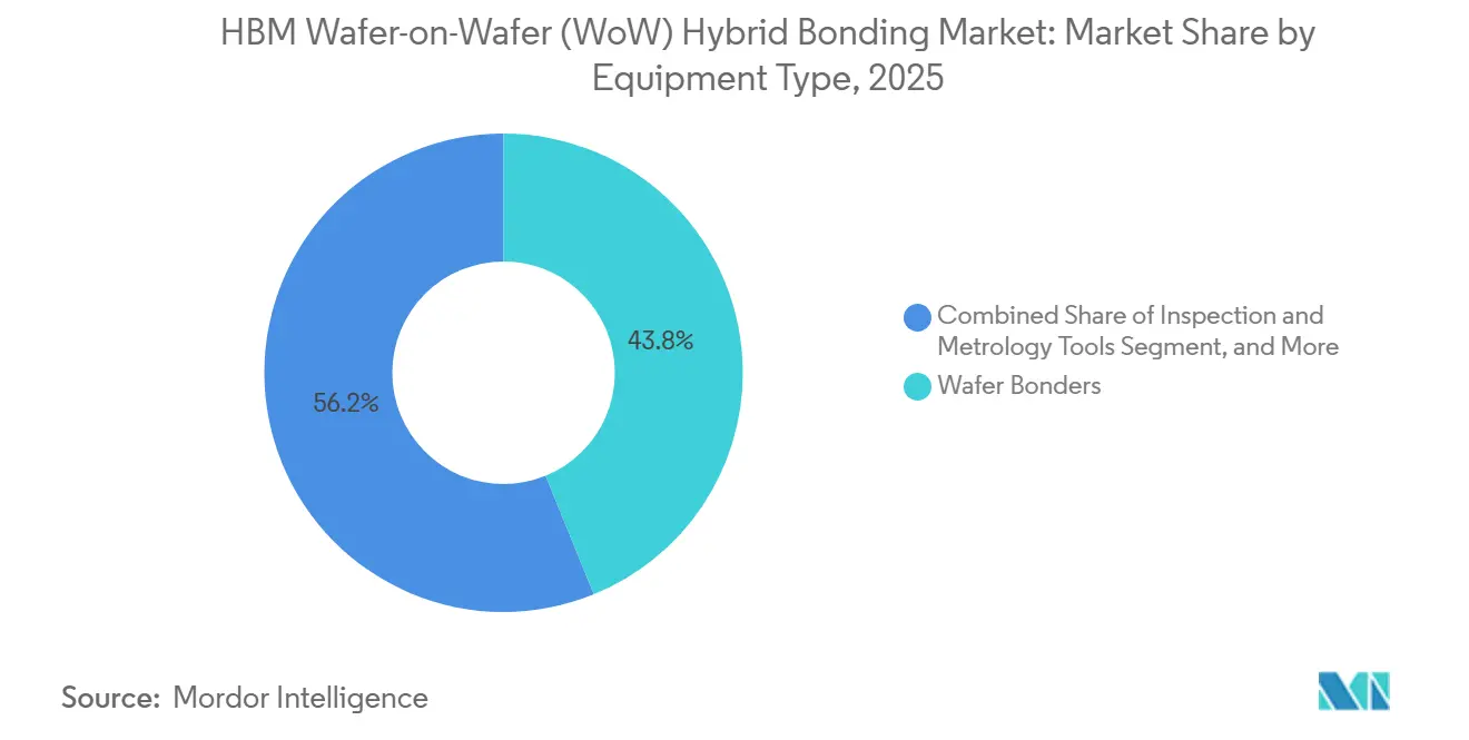
- By equipment type, wafer bonders accounted for 43.84% share of the HBM Wafer-on-Wafer (WoW) hybrid bonding market in 2025, while inspection and metrology tools are projected to advance at a 32.83% CAGR through 2031.
- By integration level, 3D integration held 62.48% share in 2025, while chiplet integration is projected to expand at a 32.58% CAGR through 2031.
- By end-user industry, semiconductor foundries accounted for 58.47% share of the HBM Wafer-on-Wafer (WoW) hybrid bonding market in 2025, while OSATs are projected to grow at a CAGR of 32.87% through 2031.
- By application, memory and storage led with 47.19% share in 2025, while computing and logic are projected to grow at a 33.08% CAGR through 2031.
- By geography, Asia-Pacific held 83.61% of the HBM Wafer-on-Wafer (WoW) hybrid bonding market share in 2025, while North America is projected to expand at a 33.02% CAGR through 2031.
Note: Market size and forecast figures in this report are generated using Mordor Intelligence’s proprietary estimation framework, updated with the latest available data and insights as of January 2026.
Market Trends and Insights
Drivers Impact Analysis of HBM Wafer-on-Wafer (WoW) Hybrid Bonding Market*
| Driver | (~) % Impact on CAGR Forecast | Geographic Relevance | Impact Timeline |
|---|---|---|---|
| Rising HBM Stack Counts in AI Accelerators | +8.2% | Global, with the highest intensity in Asia-Pacific and North America | Short term (≤ 2 years) |
| Co-Packaged Logic and Memory Integration | +6.8% | Asia-Pacific core, spill-over to North America and Europe | Medium term (2-4 years) |
| Sub-10 Micron Interconnect Pitch Migration | +5.6% | Global | Medium term (2-4 years) |
| Front-End Wafer-Level Process Control Adoption | +3.9% | Asia-Pacific and North America are leading | Short term (≤ 2 years) |
| Pilot-Line De-Risking for Chiplet-Based HBM Architectures | +2.8% | North America and Asia-Pacific | Medium term (2-4 years) |
| Photonics and Sensor Co-Integration Demand | +1.8% | North America and Europe, with early traction in the Asia-Pacific | Long term (≥ 4 years) |
| Source: Mordor Intelligence | |||
Rising HBM Stack Counts in AI Accelerators
AI accelerator roadmaps are pushing memory stack counts higher, making vertical interconnect density a central growth driver for the HBM Wafer-on-Wafer (WoW) hybrid bonding market. SK hynix unveiled a 16-layer HBM4 device with 48GB capacity and bandwidth above 2TB per second at CES 2026, and the company targeted mass production in the third quarter of 2026. Samsung disclosed HBM4 operating speeds of 11.7Gb/s by combining its 1c DRAM process with hybrid copper bonding, which placed it well above the JEDEC baseline of 8Gb/s. A peer-reviewed review in Electronics found that hybrid bonding reduced total stack height by more than 15% in an 8-layer HBM structure and improved vertical heat transfer by replacing underfill with direct copper connections. As stack counts exceed 12 layers, thermomechanical stress and package height become harder to manage with microbumps alone, so the HBM Wafer-on-Wafer (WoW) hybrid bonding market remains closely linked to next-generation AI memory programs.
Co-Packaged Logic and Memory Integration
Co-integrating logic and memory in a single bonded stack is expanding the role of the HBM Wafer-on-Wafer (WoW) hybrid bonding market beyond pure memory stacking. HKUST research showed that wafer-on-wafer stacked accelerators delivered inference up to 7.17 times faster than an NVIDIA A100 baseline, while chiplet-based designs reduced recurring engineering costs by 38.09% compared with monolithic alternatives. TSMC stated that its SoIC-X platform was used in AMD’s second-generation 3D V-Cache at 9µm pitch and delivered 10 times the bandwidth of conventional packaging. Applied Materials said its Kinex platform with Besi is already in mass production at TSMC for Broadcom custom AI ASICs, and the next-generation system targets 50nm accuracy or better with higher throughput. This combination of performance and cost benefits means the HBM Wafer-on-Wafer (WoW) hybrid bonding market can sustain demand even when pure HBM order cycles fluctuate.
Sub-10 Micron Interconnect Pitch Migration
Pitch scaling below 10µm is creating a direct technology advantage for the HBM Wafer-on-Wafer (WoW) hybrid bonding market because micro-bump approaches cannot match that density range. Tokyo Electron demonstrated 140nm pitch hybrid bonding with full-wafer alignment accuracy below 57nm misalignment, showing that the equipment roadmap is moving well beyond current production nodes. TSMC confirmed at its 2026 North America Technology Symposium that its SoIC roadmap is moving from 6µm pitch today toward 4.5µm by 2029. Each step in pitch reduction forces changes in CMP, plasma activation, dielectric deposition, and overlay metrology, so equipment refresh demand does not depend only on wafer volume growth. That recurring reinvestment cycle strengthens long-range demand visibility for the HBM Wafer-on-Wafer (WoW) hybrid bonding market.
Front-End Wafer-Level Process Control Adoption
The HBM Wafer-on-Wafer (WoW) hybrid bonding market is increasingly shaped by front-end style process control, not only by the bonding step itself. Onto Innovation described photoacoustic laser-ultrasound inspection methods that can detect voids as small as 1µm at hybrid bonding interfaces without destructive analysis, which is critical when wafers carry high value before final stack completion. EV Group launched the EVG40 D2W in September 2025 as the first dedicated die-to-wafer overlay metrology platform, with 100% die overlay measurement on 300mm wafers and throughput up to 15 times that of its predecessor.[1] As HBM generations push tighter electrical and power targets, foundries and memory manufacturers have less room to absorb variation at the bonding interface, which raises the priority of in-line metrology, cleaning, and feedback loops. That shift is changing procurement patterns across the HBM Wafer-on-Wafer (WoW) hybrid bonding market from single-tool decisions toward tightly connected process chains.
Restraints Impact Analysis of HBM Wafer-on-Wafer (WoW) Hybrid Bonding Market*
| Restraint | (~) % Impact on CAGR Forecast | Geographic Relevance | Impact Timeline |
|---|---|---|---|
| High Capital Intensity of Hybrid Bonding Tooling | -4.8% | Global | Short term (≤ 2 years) |
| Yield Sensitivity to Particle and Surface Defects | -3.9% | Global | Medium term (2-4 years) |
| Limited Qualified Supplier Base for Ultra-Precision Bonding | -3.1% | Global | Medium term (2-4 years) |
| Thermo-Mechanical Stress Risks in Ultra-Thin Stacked Dies | -2.1% | Asia-Pacific core, global for advanced logic | Long term (≥ 4 years) |
| Source: Mordor Intelligence | |||
High Capital Intensity of Hybrid Bonding Tooling
Capital intensity remains a real brake on the HBM Wafer-on-Wafer (WoW) hybrid bonding market because qualified production lines require more than a single bonder purchase. Applied Materials positioned hybrid bonding as a process chain spanning deposition, CMP, and process control, indicating that line qualification requires multiple categories of high-value equipment. SUSS MicroTec’s XBC300 Gen2 platform combines wafer-to-wafer, collective die-to-wafer, and sequential die-to-wafer capability in one system, but that modularity still sits within a broader capital program rather than a low-cost entry point. Customers also need cleaning, activation, metrology, and annealing support around the bonder, which increases the minimum spend required before commercial yields can be achieved. This keeps adoption concentrated among the most capitalized foundries, memory makers, and advanced packaging operators in the HBM Wafer-on-Wafer (WoW) hybrid bonding market.
Yield Sensitivity to Particle and Surface Defects
Yield sensitivity remains a structural restraint for the HBM Wafer-on-Wafer (WoW) hybrid bonding market because a single defect can block bond formation at fine pitch. IEEE research on Cu-Cu hybrid bonding highlighted moisture adsorption, porous bonding layers, and copper creep as difficult production failure modes during the interval between activation and bonding. Lam Research stated that nanocrystalline copper can support lower-temperature bonding by speeding copper grain diffusion, which addresses part of the thermal budget and queue-time challenge but does not remove surface sensitivity. Onto Innovation noted that as customers move toward 5-6µm pitch, wafer flatness, CMP uniformity, and oxide cleaning become progressively more critical. That means yield learning will continue to shape tool selection and ramp timing across the HBM Wafer-on-Wafer (WoW) hybrid bonding market even when end demand remains strong.
*Our forecasts treat driver/restraint impacts as directional, not additive. The impact forecasts reflect baseline growth, mix effects, and variable interactions.
HBM Wafer-on-Wafer (WoW) Hybrid Bonding Market Segment Analysis
By Bonding Architecture:
Wafer-to-Wafer Dominates as Die-to-Wafer AcceleratesWafer-to-wafer held 68.32% of the HBM Wafer-on-Wafer (WoW) hybrid bonding market share in 2025, reflecting its strong production record and higher throughput in established semiconductor applications. The architecture remained the larger part of the HBM Wafer-on-Wafer (WoW) hybrid bonding market because it can bond an entire wafer in seconds rather than placing individual dies over much longer cycle times. Its position was also supported by proven use in 3D NAND, CMOS image sensors, and DRAM, thereby reducing adoption risk for customers seeking a repeatable manufacturing route. In May 2026, imec and EV Group demonstrated less than 40nm Cu pad overlay accuracy across a full 300mm wafer at a 200nm pitch on the GEMINI FB system, demonstrating that wafer-to-wafer bonding can move into much more demanding logic stacking work.
Die-to-wafer is projected to grow at a 32.68% CAGR through 2031 because chiplet and HBM designs often need selective placement rather than full-wafer pairing. The approach is especially relevant when die sizes differ, when handling known-good dies matters, or when yield management makes full-wafer bonding inefficient. CEA-Leti demonstrated functional die-to-wafer hybrid bonding at a 1µm pitch at ECTC 2026, removing a key technical bottleneck for high-density heterogeneous AI hardware. Die-to-die bonding remained a smaller and more selective part of the HBM Wafer-on-Wafer (WoW) hybrid bonding market because its economics work best in limited-yield integration cases where single-die matching is justified.

By Bonding Type:
Copper-to-Copper Leads as Novel Interfaces Gain TractionCopper-to-Copper bonding captured 55.06% of the market share in 2025, making it the reference process in the HBM Wafer-on-Wafer (WoW) hybrid bonding market for leading-edge memory and logic applications. An IEEE research review of implementations across Sony, Samsung, TSMC, SK hynix, and Tokyo Electron confirmed that direct Cu-Cu bonding supports pitches below 10µm while offering stronger thermal and electrical performance than bump-based alternatives. That performance advantage matters in HBM and stacked logic because both interconnect density and heat transfer become harder to manage as layer counts increase. Copper-to-pad and metal-to-pad routes continue to serve as transitional options for customers moving from conventional flip-chip to more advanced bonding flows.
Oxide-to-Oxide and Metal-Oxide Hybrid Bonding is projected to grow at a 32.61% CAGR through 2031, reflecting rising interest in photonics and sensor integration, where dielectric compatibility is essential. TSMC’s SoIC-X uses an optimized SiCN dielectric with Cu pads, and imec’s 200nm pitch demonstration also used SiCN with an optimized CMP flow, demonstrating that dielectric engineering is already part of production-grade scaling. This keeps bonding type development tightly linked to surface preparation, CMP uniformity, and overlay control rather than to bond formation alone. As more heterogeneous devices move into the HBM Wafer-on-Wafer (WoW) hybrid bonding market, the gap between a simple copper interface and a full materials stack will keep narrowing.
By Equipment Type:
Wafer Bonders Lead Revenue as Inspection Tools Grow FastestWafer bonders accounted for 43.84% of revenue in 2025, making them the largest single equipment category in the HBM Wafer-on-Wafer (WoW) hybrid bonding market. EV Group’s GEMINI FB is widely regarded as a production system for hybrid and fusion bonding, while SUSS MicroTec’s XBS300 and XBC300 Gen2 offer a route spanning wafer-to-wafer and die-to-wafer process flows. Their revenue lead reflects the fact that the bonder remains the core capital item and the visible anchor of any qualified hybrid bonding line. Surface preparation tools rank behind bonders because plasma activation, CMP, and wet cleaning directly affect pre-bond surface quality and final yield.
Inspection and metrology tools are projected to expand at a 32.83% CAGR through 2031, which makes them the fastest-growing equipment segment in the HBM Wafer-on-Wafer (WoW) hybrid bonding market. Applied Materials highlighted real-time wafer condition monitoring in its Opta Quad advanced packaging CMP tool, which shows how process control is becoming embedded across the tool chain rather than handled after the fact. Onto Innovation launched the Dragonfly G5 in March 2026, with defect sensitivity down to 150nm, throughput up to 5 times that of the previous generation, and a leading HBM manufacturer selected it as the tool-of-record for the HBM4 yield ramp. That pattern shows the HBM Wafer-on-Wafer (WoW) hybrid bonding market is moving from process development into yield-optimized volume production, where inspection intensity rises with every new pitch node.
By Integration Level:
3D Integration Anchors Revenue as Chiplet Formats Scale3D integration accounted for 62.48% of the market share in 2025 and remained the largest integration layer in the HBM Wafer-on-Wafer (WoW) hybrid bonding market, as face-to-face die stacking already had commercial traction in image sensors, 3D NAND, and early DRAM use cases. AMD’s second-generation 3D V-Cache stacks 7nm SRAM on 5nm logic at a 9µm pitch using TSMC’s SoIC technology, serving as a practical proof point for larger-scale 3D adoption. That example matters because it shows hybrid bonding is already supporting commercial performance gains rather than staying limited to pilot work. The 2.5D segment continues to expand as interposer sizes become larger and advanced packaging schemes such as CoWoS and SoIC-P require multiple process steps that rely on hybrid bonding-compatible preparation and metrology.
Chiplet integration is projected to grow at a 32.58% CAGR through 2031, which makes it the fastest-growing integration format in the HBM Wafer-on-Wafer (WoW) hybrid bonding market. HKUST found that chiplet-based 3D accelerator designs reduced recurring engineering costs by 38.09% compared with monolithic alternatives, broadening their economic appeal beyond hyperscaler customers. That cost logic is relevant across compute, networking, and automotive programs where full monolithic advanced-node designs remain expensive. As chip design becomes more disaggregated, chiplet formats will keep pulling new equipment demand into the HBM Wafer-on-Wafer (WoW) hybrid bonding market.
By End-User Industry:
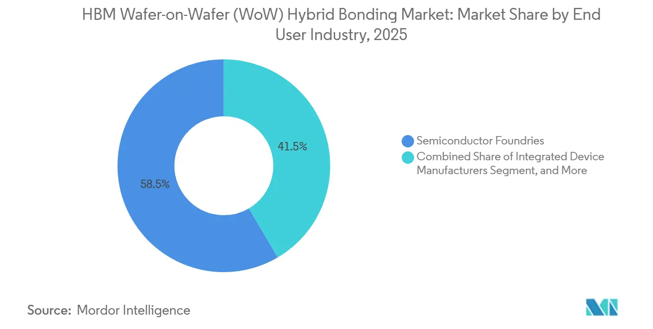
Foundries Anchor Revenue as OSATs Ramp FastestSemiconductor foundries held 58.47% of end-user revenue in 2025, which reflected TSMC’s central role in commercial wafer-on-wafer hybrid bonding through the SoIC platform. Their share stayed high because foundries combine deep process integration, customer concentration, and the balance sheet needed for long qualification cycles in the HBM Wafer-on-Wafer (WoW) hybrid bonding market. Samsung is also building internal hybrid bonding capability through its own equipment ecosystem, which shows that leading memory producers want tighter control over WoW process development for HBM4E and later nodes. Integrated device manufacturers remain meaningful because Intel’s Foveros Direct uses direct copper bonding at 10µm pitch, and CHIPS Act funding is supporting packaging-related investment at several U.S. locations.
OSATs are projected to grow at a 32.87% CAGR through 2031, making them the fastest-growing end-user segment in the HBM Wafer-on-Wafer (WoW) hybrid bonding market. Their expansion is tied to a structural shift in which foundry customers are moving front-end grade process steps into advanced packaging environments. Hanwha Semitech supplied its SHB2 Nano cluster with plasma activation, cleaning, and bonding modules to SK hynix in April 2026, demonstrating the kind of integrated, turnkey equipment OSAT-style operations will need for qualification. The remaining end-user base of research institutes and captive R&D lines stays small in revenue terms, but it remains important because pilot lines often shape future tool-of-record decisions in the HBM Wafer-on-Wafer (WoW) hybrid bonding market.
By Application:
Memory and Storage Leads While Computing and Logic OutpacesMemory and storage accounted for 47.19% of application revenue in 2025, which kept it at the center of the HBM Wafer-on-Wafer (WoW) hybrid bonding market. That lead came from HBM wafer stacking, which is the main commercial use case for the processes and equipment covered here. Samsung reported that hybrid copper bonding reduced thermal resistance by 22.8% and cut total stack height by more than 15% compared with micro-bump HBM, which explains why thermal and form-factor gains matter so much in this segment. SK hynix also confirmed progress in hybrid-bonded HBM stack development, which supports the view that memory makers are steadily moving from qualification to broader deployment.
Computing and logic are projected to grow at a 33.08% CAGR through 2031, which makes it the fastest-growing application in the HBM Wafer-on-Wafer (WoW) hybrid bonding market. ISSCC 2026 presented a hybrid-bonded 56-core DNN processor with 2.5Tb/s/mm² 3D network-on-chip bandwidth and 12.1TOPS/mm² performance density, demonstrating the scale of compute gains achievable through dense vertical integration. SEMI identified co-packaged optics and heterogeneous chiplet integration as emerging areas of advanced packaging, which support future demand for hybrid bonding across photonic-electronic combinations in the HBM Wafer-on-Wafer (WoW) hybrid bonding market.[2] Sensing and interface, connectivity and communications, and photonics and optical interconnects remained smaller in 2025, but they still represent long-cycle opportunities as co-packaged optics programs enter broader deployment from 2026 onward
Geography Analysis
APAC HBM Wafer-on-Wafer (WoW) Hybrid Bonding Market
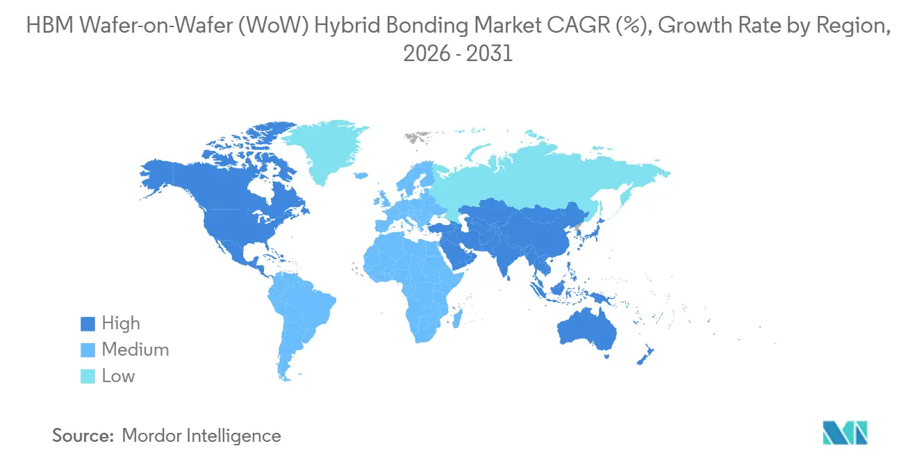
Asia-Pacific held an 83.61% share in 2025, making it the clear center of the HBM Wafer-on-Wafer (WoW) hybrid bonding market. The region leads because South Korea houses Samsung Electronics and SK hynix, Taiwan hosts TSMC’s SoIC platform, and Japan remains a major base for equipment development and materials supply.[3] This concentration keeps the HBM Wafer-on-Wafer (WoW) hybrid bonding market closely tied to a compact group of memory manufacturers, foundries, and equipment vendors that already operate at advanced-node scale. Tokyo Electron announced a USD 330 million investment in October 2025 to build a new advanced packaging equipment development hub in Kyushu, at the 2025 average exchange rate used as input. China is also building domestic alternatives in bonding-related equipment, which reflects how export controls are reshaping the supply chain and encouraging local capability development.
North America and Europe HBM Wafer-on-Wafer (WoW) Hybrid Bonding Market
North America is projected to post a 33.02% CAGR through 2031, and its HBM Wafer-on-Wafer (WoW) hybrid bonding market size is therefore set to expand faster than any other region. The main driver is the CHIPS Act-backed investment in advanced packaging and domestic semiconductor manufacturing. Intel finalized a USD 7.86 billion CHIPS Act funding award to support sites in Arizona, New Mexico, Ohio, and Oregon, including programs tied to Foveros Direct hybrid bonding. TSMC’s Arizona expansion also supports the regional case because AI customers increasingly want advanced packaging capacity inside a domestic supply chain. Europe remains smaller in share, but it stays strategically relevant through imec in Belgium, SUSS MicroTec in Germany, Besi in the Netherlands, and CEA-Leti in France.
MEA and South America HBM Wafer-on-Wafer (WoW) Hybrid Bonding Market
South America and the Middle East and Africa held only a negligible position in 2025 because they lack leading-edge semiconductor manufacturing infrastructure for this equipment class. Their role in the HBM Wafer-on-Wafer (WoW) hybrid bonding market is more likely to stay limited to service coverage and distribution support than to primary production or research activity. This means meaningful investment demand from these regions is not expected to emerge within the 2026-2031 period.
Competitive Landscape
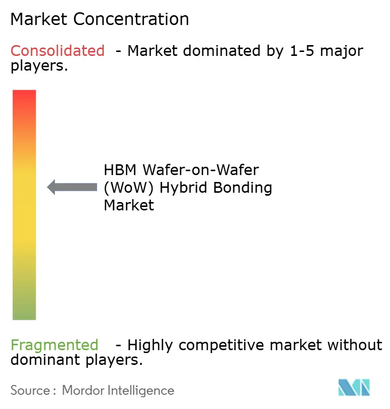
The HBM Wafer-on-Wafer (WoW) hybrid bonding market is moderately concentrated at the wafer bonder level, where EV Group and SUSS MicroTec are leading suppliers of wafer-to-wafer systems, while the Applied Materials and Besi Kinex platforms lead die-to-wafer configurations with major memory and foundry customers. This structure means competitive control is strongest inside specific tool categories rather than across the whole equipment stack. Applied Materials strengthened that position in April 2025 by taking a 9% equity stake in Besi and extending the Kinex co-development agreement, which tied front-end process capability more closely to advanced die placement and bonding precision. That move matters because customers increasingly want an integrated process relationship instead of a disconnected set of tools from separate vendors. The HBM Wafer-on-Wafer (WoW) hybrid bonding market, therefore, rewards suppliers that can anchor a full qualification flow rather than only one process step.
Tokyo Electron is positioning itself as a broader process partner by combining its existing cleaning and CMP strengths with hybrid bonding, alignment, and metrology development. It's demonstrated 140nm pitch hybrid bonding with less than 57nm misalignment, together with patent activity in in-situ bond-propagation measurement and overlay registration, signaling an attempt to control more of the yield-critical workflow. In inspection and metrology, competition is tightening around tool-of-record positions as customers prepare for HBM4 ramps. Onto Innovation strengthened its standing with the Dragonfly G5 and related AI-based analytics, while KLA continues to position CIRCL-AP within advanced packaging inspection and metrology. These moves show that software-supported yield learning is becoming a competitive layer in the HBM Wafer-on-Wafer (WoW) hybrid bonding market, not only a hardware add-on.
White-space opportunities remain in automated defect classification and in cluster-integrated annealing that can reduce queue-time sensitivity between activation and final bonding. SUSS MicroTec has expanded its position by completing a wider end-to-end hybrid bonding portfolio, including die-to-wafer capability and dedicated surface preparation clusters.[4] EV Group, meanwhile, keeps pushing overlay performance and production readiness through its GEMINI and EVG40 platforms, which helps it defend strong standing in wafer-level bonding. Regional challengers in Korea and China may increase pressure over time, but the current HBM Wafer-on-Wafer (WoW) hybrid bonding market still favors suppliers with established process credibility, customer qualification history, and the ability to scale precision at volume.
HBM Wafer-on-Wafer (WoW) Hybrid Bonding Industry Leaders
-
EV Group
-
Applied Materials, Inc.
-
SUSS MicroTec SE
-
BE Semiconductor Industries N.V.
-
ASMPT Limited
- *Disclaimer: Major Players sorted in no particular order
HBM Wafer-on-Wafer (WoW) Hybrid Bonding Market Companies Covered in this Report
- EV Group
- Applied Materials, Inc.
- SUSS MicroTec SE
- BE Semiconductor Industries N.V.
- ASMPT Limited
- Tokyo Electron Limited
- KLA Corporation
- Onto Innovation Inc.
- Lam Research Corporation
- DISCO Corporation
- SHIBAURA MECHATRONICS CORPORATION
- Hanmi Semiconductor Co., Ltd.
- Toray Engineering Co., Ltd.
- BEIJING U-PRECISION TECH CO., LTD.
- Applied Microengineering Ltd.
- SET Corporation SA
- Piotech, Inc.
- NAURA Technology Group Co., Ltd.
- Nidec Machine Tool Corporation
Recent Industry Developments in HBM Wafer-on-Wafer (WoW) Hybrid Bonding Market
- June 2026: Applied Materials unveiled a lineup of semiconductor manufacturing systems for HBM, chiplets, and hybrid bonding applications, including the Opta Quad advanced packaging CMP tool with real-time wafer condition monitoring for improved intra-wafer uniformity and total thickness variation control, and the VeritySEM 7AP electron-beam process control system for measurements on thick, warped substrates and mixed-material HBM stacks.
- June 2026: SUSS MicroTec SE shares were included in the MDAX index for the first time, reflecting the company's growing market capitalization on the back of its expanded hybrid bonding product portfolio and growing customer pipeline across 5-10 evaluation engagements.
- May 2026: Imec and EV Group demonstrated wafer-to-wafer hybrid bonding at 200nm Cu interconnect pitch with a post-bond Cu pad overlay below 40nm across a full 300mm wafer, presented at the 2026 IEEE Electronic Components and Technology Conference. The process used SiCN dielectric and an optimized CMP step on EV Group's GEMINI FB system, establishing a technology baseline for logic-to-logic stacking under imec's CMOS 2.0 paradigm.
- May 2026: CEA-Leti demonstrated a functional die-to-wafer hybrid bonding test vehicle at 1µm pitch, presented at ECTC 2026, using through-oxide via (TOV) and high-density through-silicon via (HD TSV) integration. This advance removes a key bottleneck for heterogeneous AI hardware where bandwidth per unit area must increase beyond what current 5-10µm pitch configurations can sustain.
Global HBM Wafer-on-Wafer (WoW) Hybrid Bonding Market Report Scope
The HBM Wafer-on-Wafer (WoW) Hybrid Bonding Market covers the development, production, and adoption of wafer-on-wafer hybrid bonding technologies used in high-bandwidth memory (HBM) applications. The market scope includes bonding equipment, materials, process technologies, and related integration solutions used by semiconductor manufacturers, foundries, outsourced semiconductor assembly and test providers, and memory device manufacturers to enable high-density interconnects, improved performance, and advanced packaging for HBM devices.
The HBM Wafer-on-Wafer (WoW) Hybrid Bonding Market Report is Segmented by Bonding Architecture(Wafer-to-Wafer, Die-to-Wafer, and Die-to-Die), Bonding Type (Copper-to-Copper, Copper-to-Pad and Metal-to-Pad, and Oxide-to-Oxide and Metal-Oxide Hybrid Bonding), Equipment Type (Wafer Bonders, Surface Preparation Tools, Inspection and Metrology Tools, and Cleaning and CMP Systems), Integration Level (2.5D Integration, 3D Integration, and Chiplet Integration), End-User Industry (Semiconductor Foundries, OSATs, Integrated Device Manufacturers, and Other End-user Industries), Application (Memory and Storage, Computing and Logic, Sensing and Interface, Connectivity and Communications, and Photonics and Optical Interconnects), and Geography (North America, Europe, Asia-Pacific, South America, and Middle East and Africa). The Market Forecasts are Provided in Terms of Value (USD).
Segmentation Overview
| Wafer-to-Wafer |
| Die-to-Wafer |
| Die-to-Die |
| Copper-to-Copper |
| Copper-to-Pad and Metal-to-Pad |
| Oxide-to-Oxide and Metal-Oxide Hybrid Bonding |
| Wafer Bonders |
| Surface Preparation Tools |
| Inspection and Metrology Tools |
| Cleaning and CMP Systems |
| 2.5D Integration |
| 3D Integration |
| Chiplet Integration |
| Semiconductor Foundries |
| OSATs |
| Integrated Device Manufacturers |
| Other End-user Industries |
| Memory and Storage |
| Computing and Logic |
| Sensing and Interface |
| Connectivity and Communications |
| Photonics and Optical Interconnects |
| North America | United States |
| Canada | |
| Mexico | |
| Europe | Germany |
| United Kingdom | |
| France | |
| Italy | |
| Rest of Europe | |
| Asia-Pacific | China |
| Japan | |
| South Korea | |
| Taiwan | |
| India | |
| Rest of Asia-Pacific | |
| South America | |
| Middle East and Africa |
| By Bonding Architecture | Wafer-to-Wafer | |
| Die-to-Wafer | ||
| Die-to-Die | ||
| By Bonding Type | Copper-to-Copper | |
| Copper-to-Pad and Metal-to-Pad | ||
| Oxide-to-Oxide and Metal-Oxide Hybrid Bonding | ||
| By Equipment Type | Wafer Bonders | |
| Surface Preparation Tools | ||
| Inspection and Metrology Tools | ||
| Cleaning and CMP Systems | ||
| By Integration Level | 2.5D Integration | |
| 3D Integration | ||
| Chiplet Integration | ||
| By End User Industry | Semiconductor Foundries | |
| OSATs | ||
| Integrated Device Manufacturers | ||
| Other End-user Industries | ||
| By Application | Memory and Storage | |
| Computing and Logic | ||
| Sensing and Interface | ||
| Connectivity and Communications | ||
| Photonics and Optical Interconnects | ||
| By Geography | North America | United States |
| Canada | ||
| Mexico | ||
| Europe | Germany | |
| United Kingdom | ||
| France | ||
| Italy | ||
| Rest of Europe | ||
| Asia-Pacific | China | |
| Japan | ||
| South Korea | ||
| Taiwan | ||
| India | ||
| Rest of Asia-Pacific | ||
| South America | ||
| Middle East and Africa | ||
Key Questions Answered in the Report
What is the current and forecast value of the HBM Wafer-on-Wafer (WoW) hybrid bonding space?
It stood at USD 0.39 billion in 2025 and is forecast to reach USD 2.06 billion by 2031, growing at a 32.21% CAGR over 2026-2031.
What is driving the adoption of wafer-on-wafer hybrid bonding in HBM applications?
The main driver is the move to higher HBM stack counts for AI accelerators, where finer pitch, lower thermal resistance, and reduced stack height matter more than with older micro-bump approaches.
Which region leads revenue generation in this field?
Asia-Pacific led with 83.61% share in 2025 because it combines the main HBM memory suppliers, TSMC’s SoIC platform, and a strong advanced packaging equipment base.
Which application is growing fast after memory and storage?
Computing and logic is the fastest-growing application, with a projected 33.08% CAGR through 2031, driven by 3D cache, AI inference chips, and dense logic stacking.
Why are inspection and metrology tools gaining importance?
As pitch moves toward 5-6µm and below, yield becomes highly sensitive to particles, wafer flatness, CMP uniformity, and oxide cleaning, which raises demand for in-line defect detection and overlay control.
Which end-user group is expanding fastest?
OSATs are projected to grow at a 32.87% CAGR through 2031 because advanced packaging customers are pushing more front-end grade hybrid bonding steps into outsourced packaging environments.