
HBM Silicon Interposer and Substrate Market Size and Share
Market Overview
| Study Period | 2020 - 2031 |
|---|---|
| Market Size (2026) | USD 1.62 Billion |
| Market Size (2031) | USD 5.58 Billion |
| Growth Rate (2026 - 2031) | 28.06 % |
| Fastest Growing Market | Asia-Pacific |
| Largest Market | Asia-Pacific |
| Market Concentration | Medium |
Major Players *Disclaimer: Major Players sorted in no particular order Image © Mordor Intelligence. Reuse requires attribution under CC BY 4.0. | |
HBM Silicon Interposer and Substrate Market Analysis by Mordor Intelligence
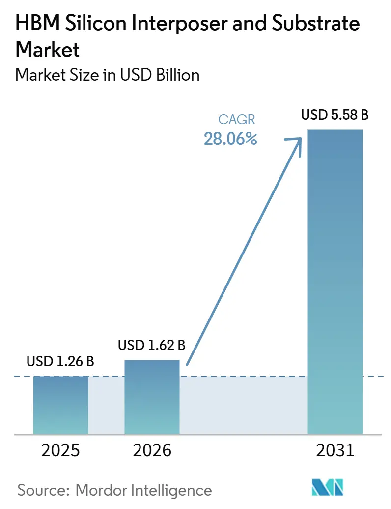
The HBM silicon interposer and substrate market size is expected to increase from USD 1.26 billion in 2025 to USD 1.62 billion in 2026 and reach USD 5.58 billion by 2031, growing at a CAGR of 28.06% over 2026-2031. The HBM silicon interposer and substrate market is being shaped by the steady rise in AI model complexity, because higher memory bandwidth and denser die-to-die links now depend on advanced interposer and substrate designs rather than conventional packaging routes. The HBM silicon interposer and substrate market also benefits from the fact that packaging has moved into the center of chip design, with interposer area, substrate layer count, and thermal stability now affecting system architecture much earlier in the development cycle. Supply remains tight across key process steps, especially as advanced substrate output, TSV qualification, and large-package handling must expand simultaneously, which keeps the HBM silicon interposer and substrate market favorable for established suppliers. The HBM silicon interposer and substrate market is also seeing a wider technology path, as hybrid bonding and glass-based approaches progress alongside mature 2.5D architectures rather than replacing them at once. Asia-Pacific remains the operating core of the HBM silicon interposer and substrate market, and that concentration gives the region clear scale advantages while also exposing the supply chain to localized bottlenecks and capacity competition.
Key Report Takeaways
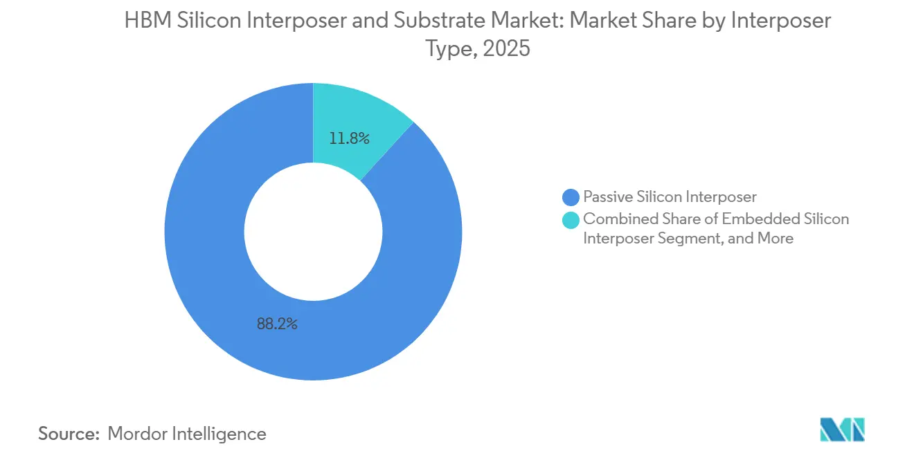
- By interposer type, passive silicon interposers held 88.21% share of the HBM silicon interposer and substrate market in 2025, while embedded silicon interposers are projected to expand at a 28.67% CAGR through 2031.
- By substrate type, organic package substrates accounted for 92.33% of segment revenue in 2025, while glass package substrates are expected to grow at a 28.85% CAGR through 2031.
- By packaging technology, 2.5D packaging captured 74.97% of segment revenue share of the HBM silicon interposer and substrate market in 2025, while hybrid bonding is projected to advance at a 28.81% CAGR through 2031.
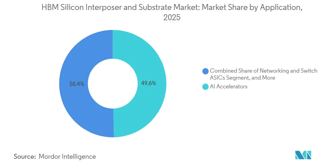
- By application, AI accelerators represented 49.64% of segment revenue in 2025, and the same segment is expected to grow at a 29.22% CAGR through 2031.
- By end user, foundries led with 48.82% of segment revenue share of the HBM silicon interposer and substrate market in 2025, and the same segment is expected to grow at a 28.74% CAGR through 2031.
- By geography, Asia-Pacific held 82.78% of revenue share of the HBM silicon interposer and substrate market in 2025 and is also projected to expand at the fastest 28.14% CAGR through 2031.
Note: Market size and forecast figures in this report are generated using Mordor Intelligence’s proprietary estimation framework, updated with the latest available data and insights as of January 2026.
Market Trends and Insights
Drivers Impact Analysis of HBM Silicon Interposer and Substrate Market*
| Driver | (~) % Impact on CAGR Forecast | Geographic Relevance | Impact Timeline |
|---|---|---|---|
| Rapid HBM Capacity Expansion in AI Accelerators | +8.5% | Global, with a concentration in Asia-Pacific, especially Taiwan and South Korea | Short term (≤ 2 years) |
| Co-Packaged Memory and Chiplet Adoption in Advanced Packaging | +5.0% | Global, with early gains in Taiwan, Japan, and North America | Medium term (2-4 years) |
| Yield Optimization Pressure in High-Layer Count Interposer Builds | +4.2% | Asia-Pacific core, with spillover to North America | Short term (≤ 2 years) |
| HBM Integration in High-Performance Data Center GPUs | +6.8% | Global, with North America-led demand and Asia-Pacific supply concentration | Short term (≤ 2 years) |
| Advanced Packaging Localization Programs in Asia-Pacific | +2.8% | Asia-Pacific, with emerging gains in India and Southeast Asia | Medium term (2-4 years) |
| Hybrid Bonding Readiness for Next-Generation HBM Stacks | +3.5% | South Korea and Taiwan | Long term (≥ 4 years) |
| Source: Mordor Intelligence | |||
Rapid HBM Capacity Expansion in AI Accelerators
Rapid HBM output growth remains the strongest demand trigger for the HBM silicon interposer and substrate market, because each AI package requires interposer capacity, advanced substrate support, and tightly qualified assembly flows rather than commodity packaging. The rise in AI accelerator deployments has made packaging availability a direct limiter on shipments, meaning interposer and substrate vendors now influence product timing in ways they did not in earlier compute cycles. This shift has strengthened the commercial position of foundries and high-end substrate makers, since customers increasingly reserve capacity well before volume production begins. It has also raised the value of process consistency, because large AI packages carry more die, more routing density, and higher thermal stress, so a weak packaging step can erase gains made at the wafer stage. As a result, the HBM silicon interposer and substrate market is no longer driven only by memory adoption, but by the speed at which the full AI package ecosystem can scale without breaking yield or reliability expectations.
HBM Integration in High-Performance Data Center GPUs
Data center GPU programs are driving the HBM silicon interposer and substrate market toward larger interposer footprints, finer routing, and denser power-delivery structures, as memory bandwidth is now a core performance variable rather than a supporting feature. HBM4 and later designs place greater functional weight on the base die and the interconnect fabric beneath the stack, increasing the importance of package-level engineering decisions. The routing burden also rises as I/O width expands and microbump pitch tightens, so interposer design becomes more closely tied to system performance, thermal behavior, and board-level integration. In practical terms, GPU developers now treat the interposer and substrate stack as part of the compute platform itself, which brings packaging decisions forward in the design cycle. That design behavior supports the HBM silicon interposer and substrate market by making advanced packaging harder to substitute late in a program and more central to long-term product roadmaps.
Co-Packaged Memory and Chiplet Adoption in Advanced Packaging
Chiplet adoption supports the HBM silicon interposer and substrate market, as disaggregated compute designs require a dense connection fabric to keep latency low while routing signals across a wider package area. As more logic is split across multiple dies, the interposer carries a larger share of system complexity, and the substrate must handle more layers, tighter warpage limits, and stricter signal integrity requirements. Research published in Microsystems and Nanoengineering showed that TSV layout patterns can materially change stress behavior at the die level, which matters as package geometry becomes more complex and more heterogeneous. The same trend makes scaling harder for new entrants, because the challenge is no longer just adding area, but controlling stress, yield, and package reliability as more active elements are brought together. This is one reason the HBM silicon interposer and substrate market continues to reward suppliers that can combine design support, front-end precision, and downstream assembly control within a single commercial offering.
Yield Optimization Pressure in High-Layer Count Interposer Builds
Yield management has become a growth driver in the HBM silicon interposer and substrate market, as customers are willing to pay for packaging approaches that reduce the risk of failure in very large, expensive AI packages. As interposer size increases and more HBM stacks are attached to a single compute package, defect tolerance falls sharply, and every incremental yield gain carries real commercial value. A 2025 study in the Journal of Semiconductor Technology and Science found that optimized TEOS SiO₂ deposition conditions improved TSV throughput while preserving robustness, demonstrating that process tuning can increase effective supply without waiting for entirely new capacity.[1] The same pressure is pushing substrate suppliers to invest more heavily in simulation, pre-assembly screening, and reliability testing, because qualification standards are becoming part of the sales proposition rather than a back-end check. In this environment, the HBM silicon interposer and substrate market grows not only from higher unit demand, but also from higher value per package as yield assurance becomes more important.
Restraints Impact Analysis of HBM Silicon Interposer and Substrate Market*
| Restraint | (~) % Impact on CAGR Forecast | Geographic Relevance | Impact Timeline |
|---|---|---|---|
| TSV Process Complexity and Long Qualification Cycles | -3.8% | Global, with the strongest effect in Taiwan and South Korea | Short term (≤ 2 years) |
| Interposer Wafer Supply Tightness and Tool Bottlenecks | -2.5% | Asia-Pacific core, with spillover to North America | Short term (≤ 2 years) |
| Thermal Warpage and Known-Good-Die Yield Loss in Large Packages | -1.8% | Global | Medium term (2-4 years) |
| High Capex for Advanced Substrate and Interposer Capacity | -1.5% | Global, with the heaviest burden on new entrants | Long term (≥ 4 years) |
| Source: Mordor Intelligence | |||
TSV Process Complexity and Long Qualification Cycles
TSV fabrication remains the clearest technical restraint on the HBM silicon interposer and substrate market, as it combines fine geometry, thermal stress exposure, and long customer qualification cycles into a single process block. The challenge grows with each HBM generation, as tighter keep-out zones and denser routing reduce the available space for design margin and process error. Research presented at IEEE IRPS 2025 showed that shrinking TSV keep-out zones can weaken BEOL reliability through electromigration and dielectric breakdown, indicating that qualification is becoming more demanding rather than easier. That technical burden slows supplier expansion, because even when capital is available, customers still require full electrical, thermal, and reliability validation before new flows enter production. The result is that the HBM silicon interposer and substrate market can show strong demand while still facing slower supply than in many adjacent semiconductor segments.
Interposer Wafer Supply Tightness and Tool Bottlenecks
Tool availability also constrains the HBM silicon interposer and substrate market, because the equipment used for etching, deposition, bonding, thinning, and TSV finishing cannot be scaled as easily as standard wafer-processing tools. This creates a gap between announced investment plans and usable output, since new lines must wait for equipment delivery, installation, process tuning, and customer qualification before they affect supply. The impact is most visible when several expansion programs move in parallel, because the same narrow equipment base must support foundries, substrate suppliers, and memory packaging operations simultaneously. Tight supply then reinforces customer concentration on proven vendors, since buyers often prefer to deepen relationships with qualified suppliers rather than take on qualification risk with unproven lines. For the HBM silicon interposer and substrate market, this means capacity additions matter, but the timing and usability of that capacity matter even more than headline capital commitments.
*Our forecasts treat driver/restraint impacts as directional, not additive. The impact forecasts reflect baseline growth, mix effects, and variable interactions.
HBM Silicon Interposer and Substrate Market Segment Analysis
By Interposer Type:
Passive Designs Lead but Active Logic Rewrites the RoadmapPassive silicon interposers accounted for 88.21% of segment revenue in 2025, making them the clear foundation of the HBM silicon interposer and substrate market across current high-volume AI and GPU packages. Their lead reflects long process learning, mature TSV integration, and compatibility with 2.5D packaging flows that already serve leading accelerator programs at scale. Passive designs also benefit from a simpler value proposition, because they deliver dense routing and HBM integration without adding logic functions that would increase process complexity and qualification work. That balance between performance and manufacturability kept passive interposers at the center of package design even as system requirements continued to rise.
The same segment still faces a structural transition, because newer HBM generations shift more control, power management, and signal handling toward the base die and the layers immediately below the memory stack. Active and embedded approaches, therefore, gain relevance when the package must do more than just route signals, especially in programs that seek tighter integration among compute dies, HBM stacks, and supporting logic. Embedded silicon interposers are projected to expand at a 28.67% CAGR through 2031, signaling that the HBM silicon interposer and substrate market is opening the door to architectures that combine routing density with added functional control. Research in Microsystems and Nanoengineering showed that TSV layout decisions can reshape die-level stress patterns, which becomes more important when interposers move from passive routing planes toward more functionally integrated designs. Even so, passive designs are likely to remain the volume anchor for much of the forecast period, because the shift toward embedded logic changes the roadmap faster than it changes the installed manufacturing base.

By Substrate Type:
ABF Hegemony Contrasts with Glass Substrate BuildoutOrganic package substrates based on ABF held 92.33% of the segment in 2025, which placed them at the center of the HBM silicon interposer and substrate market for current accelerator, GPU, and HPC package structures. ABF remains dominant because it supports high layer counts, fine redistribution, and the mechanical balance needed to pair large silicon structures with dense package routing. The segment also benefits from a strong incumbent ecosystem, where leading suppliers have already built process know-how around warpage control, yield stability, and large-format build-up designs. That installed base makes ABF the default choice for most current programs, even when customers are already studying next-generation alternatives.
Supplier investment patterns reinforce that position, since major capacity programs continue to target high-performance IC substrates rather than a sudden platform shift away from ABF. Ibiden announced a JPY 500 billion (USD 3.3 billion) investment program for high-performance IC package substrates across fiscal year 2026 to fiscal year 2028, with mass production set to begin from fiscal year 2027.[2] At the same time, glass package substrates are projected to grow at a 28.85% CAGR through 2031, because they offer a path toward better dimensional stability and lower dielectric loss in very large packages. The appeal of glass is strongest where the HBM silicon interposer and substrate market needs panel-style scaling beyond conventional reticle and warpage limits, yet commercial uptake will depend on whether suppliers can manage brittleness, via formation, and process consistency at production scale. For that reason, ABF remains the core revenue base while glass continues to define an important future option for the most demanding package formats.
By Packaging Technology:
2.5D Established, Hybrid Bonding AcceleratesThe 2.5D format accounted for 74.97% of segment revenue in 2025, making it the leading commercial architecture in the HBM silicon interposer and substrate market. Its strength comes from a practical combination of mature tooling, proven interposer integration, and compatibility with multi-die packages that need HBM placed close to the compute engine. The format also provides designers with sufficient routing density to support current AI accelerators while keeping process steps more familiar than those of many full 3D alternatives. This maturity explains why 2.5D still carries most of the commercial load even as more advanced package concepts continue to gain attention.
The growth path, however, is moving toward finer vertical and die-to-die connections that reduce height, resistance, and power loss inside increasingly dense memory stacks. Hybrid bonding is projected to grow at a 28.81% CAGR through 2031, reflecting the need for bump-free copper-to-copper links as stack counts rise and package thickness limits tighten. Research published in Springer Nature’s Moore and More found that Cu-Cu hybrid bonding can lower power consumption and reduce package thickness relative to TSV-based microbump approaches, while also supporting much finer pitch scaling. This matters for the HBM silicon interposer and substrate market because the package must now meet bandwidth, height, and thermal targets at the same time, and conventional bump structures become harder to manage as layers increase. 2.5D will remain the established base, but hybrid bonding is set to influence the performance ceiling and future design rules of the segment much more strongly over the forecast period.
By Application:
AI Accelerators Drive Volume, Adjacent Segments Define DiversificationAI accelerators accounted for 49.64% of application revenue in 2025 and are projected to grow at a 29.22% CAGR through 2031, making them the primary demand driver in the HBM silicon interposer and substrate market. These systems rely on very high memory bandwidth, dense local routing, and short signal paths between the compute die and HBM stacks, thereby increasing demand for advanced interposers and high-layer substrates. The segment also pushes package size upward, because each product cycle tends to combine more compute resources with larger or more numerous HBM stacks in the same footprint. In commercial terms, AI accelerators have made packaging a key variable in product launch timing, supply planning, and platform qualification.
The rest of the application mix matters because it broadens the addressable demand base and changes how packaging value is distributed across the HBM silicon interposer and substrate industry. Data center GPUs remain a major adjacent use case, with needs that often overlap with AI accelerators but can differ in memory intensity, workload balance, and system cost priorities. High-performance computing programs add another layer of demand, especially where custom package designs and tighter reliability screening are required for government, defense, and laboratory systems. Networking and switch ASICs extend the case for dense lateral integration, while automotive AI platforms and advanced consumer electronics widen the long-term opportunity as higher bandwidth memory reaches more endpoint categories. This wider mix does not displace AI demand, but it does make the HBM silicon interposer and substrate market less dependent on a single product class over time.
By End User:
Foundries Lead, While Fabless, OSATs, And IDMs Rebalance Value CaptureFoundries captured 48.82% of end-user revenue in 2025, which gave them the leading position in the HBM silicon interposer and substrate market. Their advantage comes from process ownership across the interposer wafer step and from their role in qualifying full package flows with end customers. When the same supplier manages a larger share of the packaging path, it captures a larger share of value and becomes harder to replace in critical programs. This is why foundries remain central even though memory makers, substrate suppliers, and OSATs all contribute important parts of the package stack.
At the same time, the value chain is shifting as more participants move earlier into package definition and more customers seek flexibility across assembly routes. Fabless companies increasingly treat interposer and substrate specifications as part of product architecture, while OSATs continue to expand their roles, with external packaging support easing pressure on constrained in-house flows. IDMs remain significant end users because memory producers still consume large volumes of interposers and substrates within their own HBM packaging operations, and Micron’s advanced packaging investment in Singapore shows how internal packaging scale has become a strategic lever rather than a support activity. The HBM silicon interposer and substrate market is therefore led by foundries today, but future value capture will depend on how design control, assembly outsourcing, and memory-side packaging expansion evolve together. That pattern points to a market where leadership is clear, but where commercial influence is spreading across more nodes of the supply chain than in earlier packaging cycles.
Geography Analysis
APAC HBM Silicon Interposer and Substrate Market
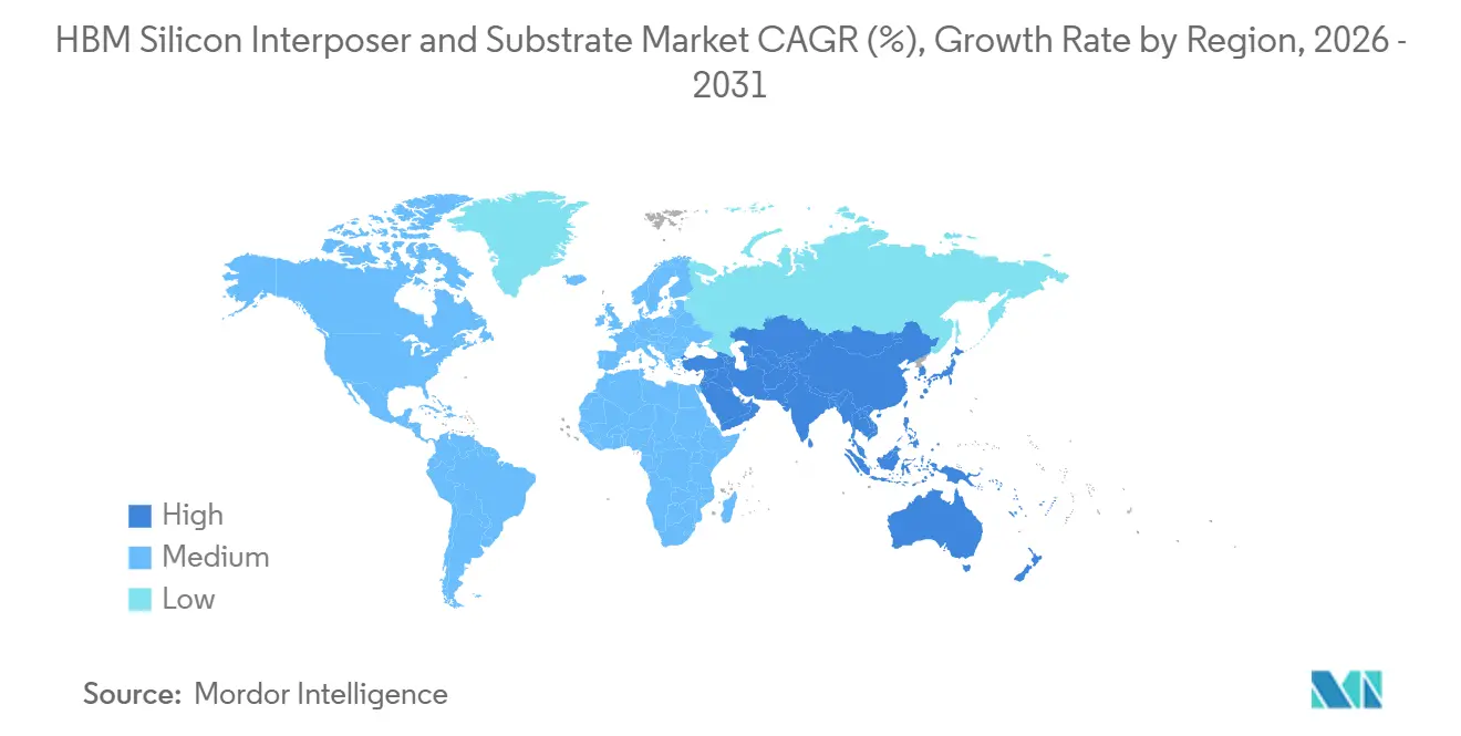
Asia-Pacific accounted for 82.78% of revenue in 2025 and is projected to expand at a 28.14% CAGR through 2031, keeping it firmly at the center of the HBM silicon interposer and substrate market. The region leads because the most critical supply chain steps are clustered across Taiwan, South Korea, Japan, and growing parts of Southeast Asia, which shortens feedback loops between foundries, memory makers, substrate suppliers, and assembly partners. Taiwan remains central through its advanced packaging leadership and deep customer qualification, while South Korea anchors HBM memory production and related packaging demand. Japan adds significant weight through its substrate materials and high-performance package substrate capabilities, which continue to support the region’s leadership in leading-edge package construction. This concentration gives Asia-Pacific scale and speed, but it also means the HBM silicon interposer and substrate market remains highly exposed to localized capacity constraints and supplier bottlenecks within the region.
North America HBM Silicon Interposer and Substrate Market
North America holds the second-largest position in the HBM silicon interposer and substrate market because many of the most important AI accelerator, GPU, and custom ASIC programs are defined there even when manufacturing remains in Asia-Pacific. The region’s strength lies in architecture ownership, customer concentration, and long-term platform roadmaps that shape what the packaging stack must deliver over multiple product generations. North American demand therefore influences interposer size, substrate complexity, and qualification priorities even when the physical package is built elsewhere. This keeps the region commercially powerful in the HBM silicon interposer and substrate market despite its smaller current manufacturing share.
EMEA, South America and APAC HBM Silicon Interposer and Substrate Market
Europe remains more selective in the HBM silicon interposer and substrate market, but it retains strategic relevance through substrate technology, engineering capability, and customer-linked expansion programs. AT&S announced up to EUR 2 billion (USD 2.32 billion), in additional expansion at Kulim in June 2026, backed by long-term customer commitments from AMD and Intel.[3] South America and the Middle East and Africa still represent a small share of the HBM silicon interposer and substrate market because they have limited advanced semiconductor manufacturing tied to interposers and high-end substrates. Southeast Asia is becoming more important as an operating base, with Micron advancing packaging and wafer fabrication in Singapore and broader capacity buildouts improving the region’s place in the packaging map.
Competitive Landscape
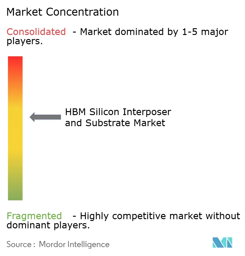
The HBM silicon interposer and substrate market has a moderately concentrated structure, with the tightest control sitting at the foundry and premium substrate tiers rather than across the full value chain. A small group of qualified suppliers still controls the most challenging steps in interposer fabrication, large-package handling, and high-layer substrate production, which keeps entry barriers high. This is especially true where customers need proven reliability on expensive AI packages, because qualification risk limits how quickly new suppliers can gain share. The HBM silicon interposer and substrate market is more fragmented at the OSAT tier, but that fragmentation does not diminish the leverage of the most established interposer and substrate players. As a result, competition is active, yet much of it still centers on expansion timing, qualification depth, and roadmap alignment rather than on price alone.
Several strategic moves since 2025 show how leading companies are positioning for the next phase of the HBM silicon interposer and substrate market. Ibiden committed JPY 500 billion (USD 3.3 billion) to expand high-performance IC package substrate supply across fiscal year 2026 to fiscal year 2028, underscoring the strong scale-up of premium substrate supply to meet AI demand. Micron also advanced its Singapore footprint through dedicated HBM packaging and wafer fabrication investments, which reflects the growing importance of internal packaging control for memory suppliers serving AI programs.[4] AT&S followed with up to EUR 2 billion (USD 2.32 billion), for Kulim expansion supported by customer commitments, showing that capacity reservation has become a key funding model in this part of the value chain.
Technology direction is widening competition inside the HBM silicon interposer and substrate market even where current supply remains concentrated. Glass-based package structures, hybrid bonding routes, and selective bridge-style approaches all aim to improve scaling economics or reduce the physical limits of current interposer designs. At the same time, customer demand for custom AI ASIC packaging creates commercial openings beyond the largest GPU programs, which may give second-tier suppliers room to grow if they can meet qualification and reliability thresholds. Even so, the HBM silicon interposer and substrate market is unlikely to become loosely fragmented in the near term, because capital intensity, process complexity, and customer qualification still favor suppliers with established scale and a long operating track record.
HBM Silicon Interposer and Substrate Industry Leaders
-
Taiwan Semiconductor Manufacturing Company Limited
-
Samsung Electronics Co., Ltd.
-
Intel Corporation
-
SK hynix Inc.
-
Micron Technology, Inc.
- *Disclaimer: Major Players sorted in no particular order
HBM Silicon Interposer and Substrate Market Companies Covered in this Report
- Taiwan Semiconductor Manufacturing Company Limited
- Samsung Electronics Co., Ltd.
- Intel Corporation
- ASE Technology Holding Co., Ltd.
- Amkor Technology, Inc.
- SK hynix Inc.
- Micron Technology, Inc.
- Fujitsu Limited
- Unimicron Technology Corp.
- Ibiden Co., Ltd.
- Shinko Electric Industries Co., Ltd.
- Kinsus Interconnect Technology Corp.
- LG Innotek Co., Ltd.
- Daeduck Electronics Co., Ltd.
- AT&S Austria Technologie und Systemtechnik AG
- Toppan Inc.
- Powertech Technology Inc.
- United Microelectronics Corporation
Recent Industry Developments in HBM Silicon Interposer and Substrate Market
- July 2026: AT&S announced an expansion of its Kulim, Malaysia manufacturing site with investments of up to EUR 2 billion (USD 2.32 billion), supported by long-term customer commitments from AMD and Intel. The expansion covers the fit-out of a second plant structure and construction of a new IC substrate core manufacturing site, with AT&S raising its fiscal 2026/27 revenue growth guidance to 45-55% in constant-currency terms as a result.
- February 2026: Ibiden announced a JPY 500 billion (USD 3.3 billion) capital investment plan across fiscal year 2026 to fiscal year 2028 for high-performance IC package substrate expansion, the largest single substrate expansion program in the industry's history. Phase one includes approximately JPY 220 billion for the Kawama Plant and additional capacity at the Ohno Plant, with mass production set to commence from fiscal year 2027.
- January 2026: Micron broke ground on an advanced wafer fabrication facility in Singapore, with its previously announced HBM advanced packaging facility confirmed as on track to contribute meaningfully to HBM supply in calendar year 2027.
- April 2025: LG Innotek inaugurated its "Dream Factory" FC-BGA substrate production facility in Gumi, South Korea, establishing a high-automation manufacturing hub targeting USD 700 million in FC-BGA substrate revenue by 2030. The facility employs AI-based quality management systems that enable real-time defect detection and correction throughout the FC-BGA production process.
Global HBM Silicon Interposer and Substrate Market Report Scope
The HBM silicon interposer and substrate market encompasses the design, manufacturing, and supply of silicon interposers and advanced substrates used to integrate high-bandwidth memory (HBM) with processors, accelerators, and other semiconductor devices. The market scope includes silicon interposers, organic substrates, and related packaging platforms used across applications such as artificial intelligence, high-performance computing, data centers, graphics processing, networking, and advanced consumer electronics.
The HBM Silicon Interposer and Substrate Market Report is Segmented by Interposer Type (Passive Silicon Interposer, Active Silicon Interposer, and Embedded Silicon Interposer), Substrate Type (Organic Package Substrate, Glass Package Substrate, Silicon Bridge/Silicon Carrier, and Other Substrate Types), Packaging Technology (2.5D Packaging, 3D Packaging, Chiplet Packaging, and Hybrid Bonding), Application (AI Accelerators, Data Center GPUs, High Performance Computing, Networking and Switch ASICs, Automotive AI Platforms, and Consumer Electronics), End User (Integrated Device Manufacturers (IDMs), Fabless Semiconductor Companies, OSATs, and Foundries), and Geography (North America, Europe, Asia-Pacific, South America, and Middle East and Africa). The Market Forecasts are Provided in Terms of Value (USD).
Segmentation Overview
| Passive Silicon Interposer |
| Active Silicon Interposer |
| Embedded Silicon Interposer |
| Organic Package Substrate |
| Glass Package Substrate |
| Silicon Bridge/Silicon Carrier |
| Other Substrate Types |
| 2.5D Packaging |
| 3D Packaging |
| Chiplet Packaging |
| Hybrid Bonding |
| AI Accelerators |
| Data Center GPUs |
| High Performance Computing |
| Networking and Switch ASICs |
| Automotive AI Platforms |
| Consumer Electronics |
| Integrated Device Manufacturers (IDMs) |
| Fabless Semiconductor Companies |
| OSATs |
| Foundries |
| North America | United States |
| Canada | |
| Mexico | |
| Europe | Germany |
| United Kingdom | |
| France | |
| Italy | |
| Rest of Europe | |
| Asia-Pacific | China |
| Japan | |
| South Korea | |
| Taiwan | |
| India | |
| Rest of Asia-Pacific | |
| South America | |
| Middle East and Africa |
| By Interposer Type | Passive Silicon Interposer | |
| Active Silicon Interposer | ||
| Embedded Silicon Interposer | ||
| By Substrate Type | Organic Package Substrate | |
| Glass Package Substrate | ||
| Silicon Bridge/Silicon Carrier | ||
| Other Substrate Types | ||
| By Packaging Technology | 2.5D Packaging | |
| 3D Packaging | ||
| Chiplet Packaging | ||
| Hybrid Bonding | ||
| By Application | AI Accelerators | |
| Data Center GPUs | ||
| High Performance Computing | ||
| Networking and Switch ASICs | ||
| Automotive AI Platforms | ||
| Consumer Electronics | ||
| By End User | Integrated Device Manufacturers (IDMs) | |
| Fabless Semiconductor Companies | ||
| OSATs | ||
| Foundries | ||
| By Geography | North America | United States |
| Canada | ||
| Mexico | ||
| Europe | Germany | |
| United Kingdom | ||
| France | ||
| Italy | ||
| Rest of Europe | ||
| Asia-Pacific | China | |
| Japan | ||
| South Korea | ||
| Taiwan | ||
| India | ||
| Rest of Asia-Pacific | ||
| South America | ||
| Middle East and Africa | ||
Key Questions Answered in the Report
How large is the HBM silicon interposer and substrate opportunity through 2031?
The HBM silicon interposer and substrate market is projected to grow from USD 1.62 billion in 2026 to USD 5.58 billion by 2031, at a 28.06% CAGR.
Which application generates the most demand for advanced interposers and substrates?
AI accelerators lead the application mix with 49.64% share in 2025 and are also expected to post the fastest 29.22% CAGR through 2031.
Why does Asia-Pacific dominate this space?
Asia-Pacific accounted for 82.78% of revenue in 2025 because foundry packaging, HBM memory production, and premium substrate supply are concentrated in Taiwan, South Korea, and Japan.
Which substrate platform is most important today?
ABF-based organic package substrates remain the core platform with 92.33% segment share in 2025 because they support high layer counts and established manufacturing flows.
What packaging technology is growing fastest for next-generation HBM stacks?
Hybrid bonding is expected to expand at a 28.81% CAGR through 2031 as it helps reduce package height, lower power loss, and support finer interconnect pitch.
What is the main supply-side risk for this field?
The biggest constraints come from TSV complexity, long qualification cycles, and tool bottlenecks, which slow the pace at which new interposer and substrate capacity can become production-ready.