
HBM Manufacturing Equipment Market Size and Share
Market Overview
| Study Period | 2020 - 2031 |
|---|---|
| Market Size (2026) | USD 1.67 Billion |
| Market Size (2031) | USD 4.98 Billion |
| Growth Rate (2026 - 2031) | 24.42 % |
| Fastest Growing Market | Asia-Pacific |
| Largest Market | Asia-Pacific |
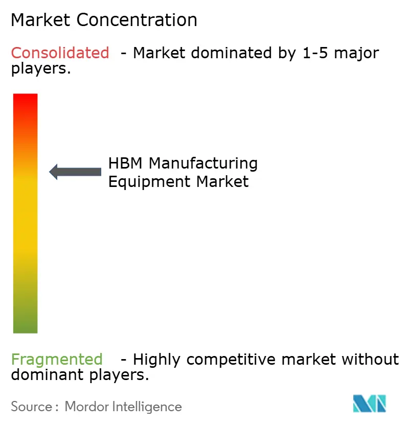
| Market Concentration | Medium |
Major Players *Disclaimer: Major Players sorted in no particular order Image © Mordor Intelligence. Reuse requires attribution under CC BY 4.0. | |
HBM Manufacturing Equipment Market Analysis by Mordor Intelligence
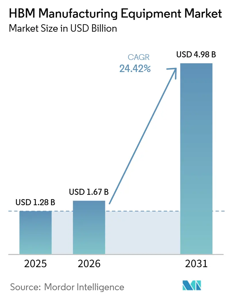
The HBM manufacturing equipment market size is expected to increase from USD 1.28 billion in 2025 to USD 1.67 billion in 2026 and reach USD 4.98 billion by 2031, growing at a CAGR of 24.40% over 2026-2031. The HBM manufacturing equipment market is being shaped by the shift from conventional DRAM packaging toward taller memory stacks that need tighter alignment, thinner dies, and cleaner interfaces at every step. This is driving up tool demand across bonding, TSV formation, planarization, and inspection, because each new stack generation incurs a higher yield penalty when process control slips. Competitive positioning is also shifting, as suppliers with process-of-record status in core steps are holding an advantage during qualification cycles that remain long and costly for new entrants. The HBM manufacturing equipment market is also expanding its demand base beyond memory companies, as foundries become more involved as logic-rich base dies move deeper into advanced-node production. This keeps the opportunity set strongest for vendors that can support both current thermocompression production lines and the coming transition toward hybrid bonding.
Key Report Takeaways
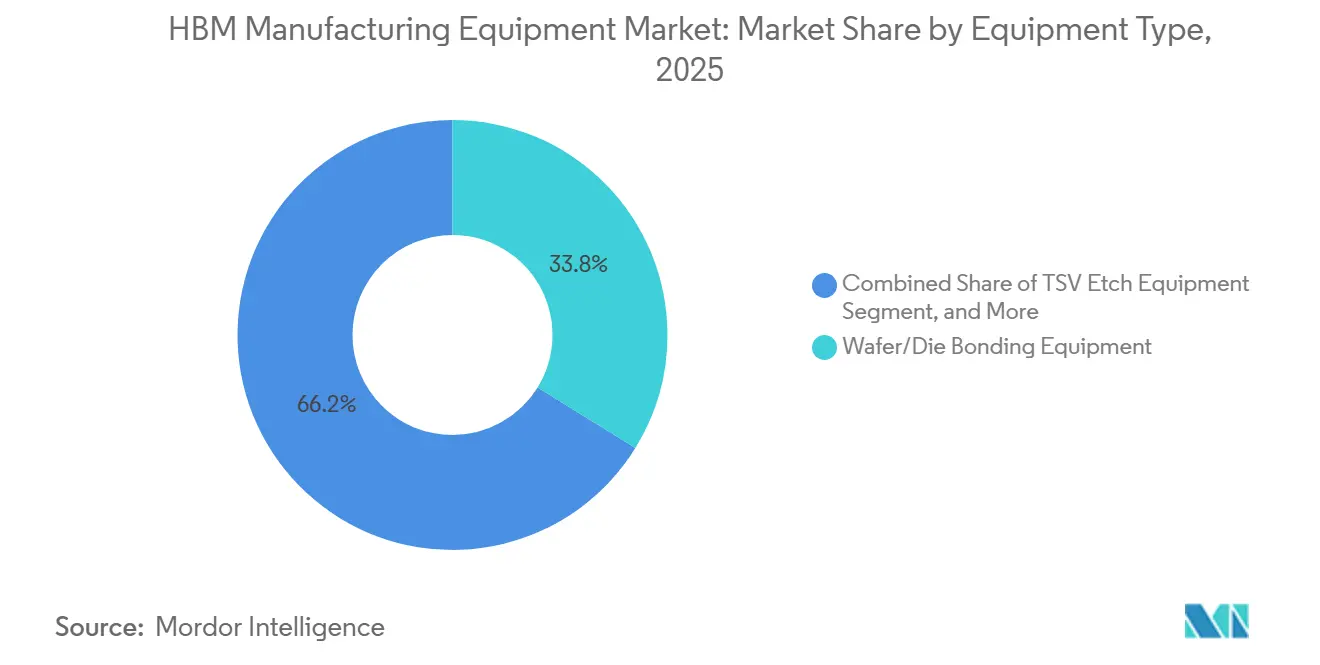
- By equipment type, Wafer/Die Bonding Equipment held the largest share at 33.81% in 2025, while Temporary Bonding and Debonding Equipment is projected to expand at a 25.38% CAGR through 2031 in the HBM manufacturing equipment market.
- By bonding technology, thermocompression bonding led with a 72.46% share in 2025, while hybrid bonding is projected to grow at a 25.89% CAGR through 2031 in the HBM manufacturing equipment market.
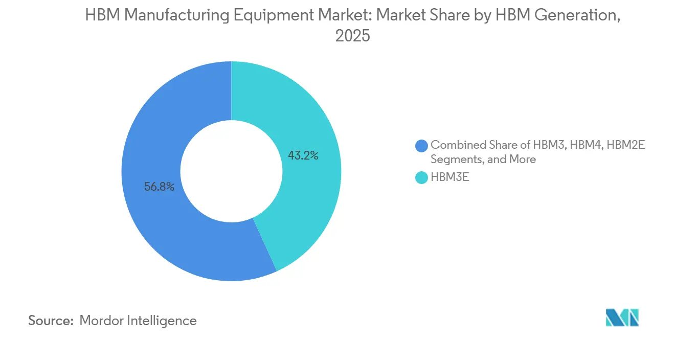
- By HBM generation, HBM3E accounted for 43.19% of revenue in 2025, while HBM4 is projected to expand at a 25.32% CAGR through 2031 in the HBM manufacturing equipment market.
- By stacking method, die-to-wafer held 62.26% share in 2025, while wafer-to-wafer is projected to advance at a 25.72% CAGR through 2031 in the HBM manufacturing equipment market.
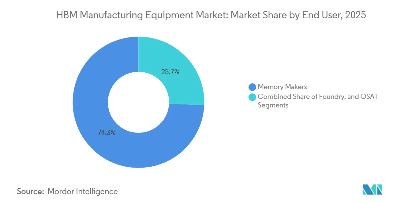
- By end user, memory makers represented 74.29% of demand in 2025, while foundries are projected to record the fastest growth at a 25.66% CAGR through 2031 in the HBM manufacturing equipment market.
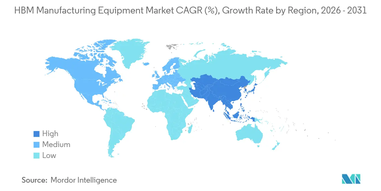
- By geography, Asia-Pacific accounted for 82.14% share of the HBM manufacturing equipment market in 2025 and is also projected to remain the fastest-growing region, with a 25.28% CAGR through 2031.
Note: Market size and forecast figures in this report are generated using Mordor Intelligence’s proprietary estimation framework, updated with the latest available data and insights as of January 2026.
Market Trends and Insights
Drivers Impact Analysis of HBM Manufacturing Equipment Market*
| Driver | (~) % Impact on CAGR Forecast | Geographic Relevance | Impact Timeline |
|---|---|---|---|
| AI Memory Stack Density Driving TSV And Hybrid Bonding Tool Demand | +7.2% | Global, concentrated in South Korea, Taiwan, and Japan | Short term (≤ 2 years) |
| Migration To HBM4 And Lower-Pitch Interconnects | +5.5% | South Korea, Taiwan, Japan, with secondary demand in North America | Short term (≤ 2 years), Medium term (2–4 years) |
| Advanced Packaging Capacity Additions By Memory Makers | +4.3% | South Korea, Japan, United States | Medium term (2-4 years) |
| Rising Need For Ultra-Flat Surfaces And Defect-Free Interfaces | +2.6% | Global | Medium term (2-4 years) |
| Localization Of Advanced Semiconductor Equipment Supply Chains | +1.8% | United States, Japan, Europe, India | Long term (≥ 4 years) |
| Process Integration Across TSV Etch, Bonding, And CMP Platforms | +1.3% | Global | Medium term (2-4 years) |
| Source: Mordor Intelligence | |||
AI Memory Stack Density Driving TSV And Hybrid Bonding Tool Demand
The HBM manufacturing equipment market is now tied more closely to AI accelerator deployment than to the older DRAM replacement cycle. Higher AI model complexity is pushing memory stacks toward denser TSV arrays, tighter bonding pitch, and more demanding planarization steps, which raises equipment intensity per wafer start. Applied Materials introduced the Nokota Vmax 2 electrochemical deposition tool with adaptive pattern tuning to address plating variation across TSV arrays at very fine pitch nodes. This matters because defects that were manageable at earlier geometries can now reduce yield across an entire multi-die stack. The HBM manufacturing equipment market is therefore seeing demand that follows compute roadmaps, as NVIDIA's Rubin platform specification for 8 HBM4 stacks and 22 terabytes per second of aggregate bandwidth is already influencing supplier planning. That combination makes tool demand both visible and durable through the forecast period.
Migration To HBM4 And Lower-Pitch Interconnects
HBM4 is raising the technical bar for the HBM manufacturing equipment market by moving to a 2,048-bit interface and pushing per-stack bandwidth above 2 terabytes per second. Those changes require tools that can handle individual DRAM dies measuring nearly 30 micrometers thick while maintaining alignment within sub-100-nanometer tolerances across the full stack. Besi stated in its Q1 2026 discussion that all 3 major memory manufacturers are evaluating hybrid bonding tools to the same customer requirement, with commercial deployment of hybrid-bonded stacks targeted for 2027. The transition is also expanding demand in Taiwan, as HBM4 base dies are being fabricated on advanced logic nodes at TSMC rather than remaining entirely within traditional memory flows. That changes the tool mix, since bonding, CMP, metrology, and TSV steps now need to satisfy both memory and foundry qualification standards. The HBM manufacturing equipment market is therefore being reshaped not only by higher stack counts, but also by the broader process integration required to support logic-rich base dies.
Advanced Packaging Capacity Additions By Memory Makers
The HBM manufacturing equipment market continues to depend heavily on the capital plans of SK hynix, Samsung Electronics, and Micron Technology. These companies have committed to unusually large multiyear spending programs, and that is giving equipment suppliers better order visibility than in many earlier semiconductor cycles. Micron raised its fiscal 2026 capital expenditure guidance to USD 20 billion, up 45% from the prior year. In July 2026, Samsung Electronics and SK hynix announced investments in the Chungcheong region, with SK hynix specifically investing in advanced packaging tied to HBM back-end processing. This concentration of capacity buildout in South Korea and Japan is creating local demand clusters where delivery windows are extending, and incumbent suppliers are gaining protection from near-term share disruption. The HBM manufacturing equipment market is benefiting because these factory plans are translating into multi-step tool orders rather than into single-line purchases.
Rising Need For Ultra-Flat Surfaces And Defect-Free Interfaces
The HBM manufacturing equipment market is seeing stronger demand for CMP, metrology, and inspection because hybrid bonding works only when surfaces are extremely flat and interfaces remain nearly defect-free. At pitches of 9 micrometers or less, copper-to-copper direct bonding requires surface roughness below 0.5 nanometers and alignment accuracy within 100 nanometers, leaving little tolerance for process drift. Applied Materials stated that its Opta Quad advanced packaging CMP tool monitors wafer conditions in real time during polishing to improve intra-wafer uniformity and thickness control for advanced packaging flows. KLA reported advanced packaging business revenue above USD 850 million in 2025, supported by rising demand for inspection in TSV, hybrid bonding, and redistribution layer steps.[1] This shows that inspection is no longer acting as a final checkpoint alone, because it is becoming part of continuous yield management across the full packaging line. As a result, the HBM manufacturing equipment market is creating recurring process-control demand that extends beyond initial tool placement.
Restraints Impact Analysis of HBM Manufacturing Equipment Market*
| Restraint | (~) % Impact on CAGR Forecast | Geographic Relevance | Impact Timeline |
|---|---|---|---|
| Extreme Capex Intensity And Long Qualification Cycles | -2.8% | Global | Medium term (2-4 years) |
| Yield Sensitivity In High-Aspect-Ratio TSV And Hybrid Bonding Flows | -2.2% | Global, concentrated in Asia-Pacific | Short term (≤ 2 years) |
| Limited Installed Base Outside Leading Memory Hubs | -1.5% | North America, Europe, South America, Middle East and Africa | Long term (≥ 4 years) |
| Tool Interface Fragmentation Across Memory Makers And OSATs | -1.0% | Global | Medium term (2-4 years) |
| Source: Mordor Intelligence | |||
Extreme Capex Intensity And Long Qualification Cycles
A major limit on the HBM manufacturing equipment market is the high cost of next-generation bonding systems and the long qualification cycle needed before those tools can support production yield. That cost structure slows procurement even when device demand is strong, because tool decisions must be matched with long validation periods inside customer fabs. The burden is also uneven, since large memory makers with established process relationships can move faster than new packaging entrants or OSATs. In some cases, new participants may face qualification timelines of more than 18 months before a line becomes production-ready. The HBM manufacturing equipment market, therefore, grows more slowly than end demand alone would suggest, because capex discipline and qualification risk narrow the customer set.
Yield Sensitivity In High-Aspect-Ratio Tsv And Hybrid Bonding Flows
Yield sensitivity remains a real brake on the HBM manufacturing equipment market, as a single defect in a TSV or bonding interface can compromise the performance of the entire memory stack. High-aspect-ratio TSVs with depth-to-diameter ratios of 10 to 1 or higher create etch-and-fill challenges that are harder to control as stacks get taller. Tokyo Electron's 2026 patent activity on step-ramp grading for hybrid bonding reflected the need to improve copper coupling and reduce latent failure risks in 16-high and larger stacks. Tokyo Electron also noted in its 2025 science report that hybrid bonding manufacturing costs remained 2 to 3 times higher than flip-chip bonding per die, mainly due to yield variability rather than material costs.[2] This means line ramps can stall even after equipment has been installed, and suppliers may see order timing shift by quarters when customer yield learning slows. The HBM manufacturing equipment market stays attractive, but actual shipment conversion depends heavily on how fast producers stabilize these advanced flows.
*Our forecasts treat driver/restraint impacts as directional, not additive. The impact forecasts reflect baseline growth, mix effects, and variable interactions.
HBM Manufacturing Equipment Market Segment Analysis
By Equipment Type:
Wafer Bonding Leads While Debonding Tools Scale FastestWafer/Die Bonding Equipment held 33.81% of the HBM manufacturing equipment market share in 2025, which made it the largest equipment category in current production lines. Its lead came from HBM3E volume manufacturing across SK hynix, Samsung, and Micron, where thermocompression bonders remain the central tool for die stacking. This position is also supported by long qualification cycles, because a fully approved bonding tool is difficult to displace once it is embedded in a high-volume line. TSV Etch Equipment and CMP Equipment followed as important linked process categories, since etch forms the via structure and CMP prepares the surface for later bonding stages. The HBM manufacturing equipment market continues to reward vendors that can support both throughput and repeatability in these tightly linked steps.
Temporary Bonding and Debonding Equipment is projected to grow the fastest, at a 25.38% CAGR from 2026 to 2031, reflecting the move toward thinner DRAM dies and taller stack designs. EV Group said its IR Layer Release technology enables nanometer-level precision laser debonding of silicon and eliminates the need for glass substrates in advanced temporary bonding flows.[3] That matters because handling dies below 30 micrometers becomes more difficult as stack counts rise and wafer thinning intensifies. SUSS MicroTec has maintained a strong position in temporary bonding and debonding, which makes it relevant to both today's HBM ramps and future wafer-level stacking programs. Interoperability across these tool sets is becoming more important as customers try to reduce integration time across complex packaging flows. That is why the HBM manufacturing equipment industry is placing greater value on suppliers that can fit into an existing line without creating new process friction. The HBM manufacturing equipment market is therefore expanding not only through higher tool counts, but also through the growing need for compatible multi-step platforms.

By Bonding Technology:
Thermocompression Dominates As Hybrid Bonding Gains GroundThermocompression bonding accounted for 72.46% of the HBM manufacturing equipment market in 2025, reflecting its near-universal use across HBM3E production. It remains the production standard because it can support stacked DRAM assembly at pitches of 9 to 55 micrometers with known heat and pressure control profiles. This shows how single-customer exposure can still define the economics of a major bonding supplier in the HBM manufacturing equipment market. Temporary wafer bonding and debonding also grow alongside thermocompression lines because it enables safer handling during grinding, TSV exposure, and metallization.
Hybrid bonding is projected to grow at a 25.89% CAGR from 2026 to 2031, making it the fastest-growing bonding technology as stack heights exceed current thermocompression limits. SUSS MicroTec introduced the XBC300 Gen2 D2W platform as an integrated system covering wafer-to-wafer, collective die-to-wafer, and sequential die-to-wafer bonding with alignment accuracy of plus or minus 100 nanometers. Samsung is developing hybrid bonding internally through SEMES, while Besi has already shipped evaluation units to all 3 major memory manufacturers. The shift is important because zero-gap copper-to-copper bonding allows higher bandwidth density per unit area than bump-based interconnects. Adoption will still move in phases, since hybrid bonding costs remain 2 to 3 times those of flip-chip bonding per die and must come down through yield improvement. The HBM manufacturing equipment industry is therefore entering a period where both legacy and next-generation bonding lines will coexist. That coexistence keeps the HBM manufacturing equipment market attractive for vendors that can serve current mass production while also securing future qualification wins.
By HBM Generation:
HBM3E Leads Production While HBM4 Reshapes Equipment RoadmapsHBM3E accounted for 43.19% of revenue in 2025, which made it the largest generation in active equipment demand. Its installed base is tied to production-grade deployment on NVIDIA H100 and Blackwell-class accelerators, which has kept tool demand centered on thermocompression bonders and mature MR-MUF process steps. HBM2 and HBM2E are losing relevance in new equipment spending because customer investment has moved toward higher-bandwidth platforms. HBM3 still supports selected AI deployments, but it does not require the same scale of fresh capital spending because much of the installed base is already in place. The HBM manufacturing equipment market, therefore, remains anchored in HBM3E today even as customer roadmaps are shifting beyond it.
HBM4 is projected to grow at a 25.32% CAGR from 2026 to 2031, making it the fastest-rising generation in future equipment spending. NVIDIA's Rubin platform design calls for 8 HBM4 stacks delivering 288 gigabytes of memory and 22 terabytes per second of aggregate bandwidth per GPU. Applied Materials said its Producer Avila 2 PECVD tool deposits stress-balanced dielectric films around TSVs to reduce die warpage in 12-high, 16-high, and taller HBM configurations. That kind of capability did not carry the same weight in the HBM3E cycle, which shows how the equipment roadmap is changing with stack complexity. HBM4E is already entering early planning discussions, and Samsung has publicly tied that future generation to hybrid bonding adoption. The HBM manufacturing equipment market is therefore seeing demand from before full commercial launch, because suppliers must qualify tools well ahead of volume ramps. This also means customer purchase decisions are becoming more forward-looking than in earlier memory generations.
By Stacking Method:
Die-To-Wafer Prevails As Wafer-To-Wafer AcceleratesDie-to-wafer held 62.26% of the HBM manufacturing equipment market share in 2025, making it the leading stacking method in current commercial use. It leads because known-good dies can be selected one by one, reducing the yield loss that would result from bonding a full wafer to a defective base die. Hanwha Semitech delivered its SHB2 Nano die-to-wafer hybrid bonding cluster system to SK hynix in April 2026 for qualification. The tool combined plasma activation, DI cleaning, and bonding modules from multiple suppliers. That shows how modern D2W systems are functioning as integrated process environments rather than as single-step machines. Die-to-die stacking remains a smaller niche because it is better suited to highly customized high-performance configurations than to mainstream HBM manufacturing volumes.
Wafer-to-wafer is projected to expand at a 25.72% CAGR through 2031 and is the fastest-growing stacking method in the HBM manufacturing equipment market. Its appeal lies in higher throughput potential, as alignment and bonding occur at the wafer level rather than through repeated die-handling steps. EV Group said its GEMINI FB production wafer bonding system was designed for wafer-to-wafer environments with strong throughput and overlay control for advanced integration flows. The shift will likely gather pace after HBM4E, when the economics of 20-high stacks begin to favor wafer-level productivity more clearly. That transition is still several years away from broad production, but vendors are already adjusting roadmaps around it. SUSS MicroTec, EV Group, and Tokyo Electron are all aligning product development to that future requirement. The HBM manufacturing equipment market is therefore balancing today's yield-first preference for D2W with a future throughput case for W2W.
By End User:
Memory Makers Control Volume Spend While Foundries Record The Fastest RiseMemory makers accounted for 74.29% of demand in 2025, making them the clear center of procurement in the HBM manufacturing equipment market. SK hynix, Samsung Electronics, and Micron continue to account for the bulk of equipment purchases because they control the core HBM production lines and near-term packaging ramps. Their capital spending plans have become more visible through public disclosures, which gives major suppliers a clearer line of sight than in many prior memory cycles. Samsung's equipment ordering activity for its P5 HBM fab and Micron's USD 20 billion fiscal 2026 capex plan both support that improved visibility. OSATs still hold a smaller share, but their role is growing as memory makers look for ways to reduce the concentration of back-end capital spending.
Foundries are projected to expand at a 25.66% CAGR in the HBM manufacturing equipment market through 2031, making them the fastest-growing end-user category. The driver is structural, because HBM4 shifts more base-die logic fabrication to TSMC and other advanced-node foundries. That pulls foundries into procurement for TSV etch, advanced CMP, and hybrid bonding steps that had previously been concentrated inside memory companies. The HBM manufacturing equipment market is therefore developing a second major buyer group rather than relying only on traditional DRAM players. This change also raises the qualification bar, since foundries tend to apply tighter process control expectations drawn from leading-edge logic production. Some suppliers that were historically strongest in memory are already adapting their platforms to gain credibility in foundry-grade packaging environments. The HBM manufacturing equipment industry now has to serve both memory-centric and logic-centric procurement models simultaneously. That widens the addressable market, but it also increases the risk for suppliers that do not translate well across both customer types.
Geography Analysis
APAC HBM Manufacturing Equipment Market
Asia-Pacific accounted for 82.14% of the HBM manufacturing equipment market size in 2025 and is projected to grow at a 25.28% CAGR through 2031. South Korea remains the center of this regional position because it combines the largest HBM production base with major new commitments in packaging and fabrication. Taiwan is becoming increasingly important because TSMC's advanced foundry services are driving HBM base-die production onto logic-intensive manufacturing lines. Japan also plays a dual role through domestic equipment suppliers such as SCREEN, DISCO, ULVAC, and Tokyo Electron, as well as through Micron's HBM expansion in Hiroshima. The HBM manufacturing equipment market stays concentrated in Asia-Pacific because the region combines memory production, supplier density, and established qualification infrastructure. China is still building a more separate domestic ecosystem, but export controls on advanced packaging tools continue to limit its access to global best-in-class equipment. That is creating a parallel path for local tool development rather than a direct challenge to incumbent suppliers across the main regional demand centers.
North America and Europe HBM Manufacturing Equipment Market
North America still holds a much smaller share than Asia-Pacific in the current HBM manufacturing equipment market, but its long-term role is strengthening as U.S. semiconductor incentives support new capacity. Micron's plan to build major manufacturing capacity in Onondaga County, New York, along with expansion in Boise, shifts the United States toward a more meaningful future demand center for bonding, TSV, and advanced packaging tools. Europe contributes less through memory production and more through supplier strength, especially through EV Group in Austria and SUSS MicroTec in Germany. EV Group remains central in wafer bonding and layer transfer, while SUSS MicroTec is advancing hybrid bonding capabilities that align with the next stage of the HBM manufacturing equipment market. Besi in the Netherlands also holds a strategically important place because all 3 major memory producers are evaluating its hybrid bonding tools.
The Americas, EMEA and APAC HBM Manufacturing Equipment Market
South America, the Middle East, and Africa account for only a minimal share of current demand in the HBM manufacturing equipment market. Neither region has a major installed base of HBM fabrication or advanced packaging capacity, so equipment spending remains limited to smaller testing and electronics assembly needs. Government semiconductor programs in parts of the Gulf and electronics incentive frameworks in Brazil could support longer-term packaging activity, but meaningful HBM-specific procurement remains beyond the current forecast window. The HBM manufacturing equipment market, however, is geographically concentrated, with the main competitive and investment actions still centered on Asia-Pacific and selected projects in North America and Europe.
Competitive Landscape
The HBM manufacturing equipment market operates as a process-led oligopoly, with a limited set of global suppliers controlling the most critical steps, while a wider group of specialists competes in adjacent process areas. Applied Materials, Lam Research, Tokyo Electron, KLA, EV Group, and SUSS MicroTec hold strong positions across etch, CMP, bonding, inspection, and temporary bonding workflows. A second tier, including Hanmi Semiconductor, Besi, ASMPT, SCREEN Holdings, DISCO, ULVAC, Ebara, Hanwha Semitech, and YC Corporation, is active in narrower but still high-value parts of the line. The HBM manufacturing equipment market favors these suppliers because process-of-record status tends to stay in place once a tool is qualified at a leading memory manufacturer. That makes engineering credibility and field performance more important than aggressive pricing during early customer selection.
One clear strategic move has been the Kynex hybrid bonding platform developed by Applied Materials and Besi, which shows how front-end and back-end tool makers are combining capabilities to pursue next-generation bonding positions. Applied Materials reported fiscal 2025 revenue of USD 28.37 billion, with HBM-specific equipment revenue of USD 1.5 billion, underscoring the category's importance to a major equipment supplier.[4] A second example is SUSS MicroTec's XBC300 Gen2 D2W platform, which combined wafer-to-wafer, collective die-to-wafer, and sequential die-to-wafer modes into a single cluster and positioned the company for future hybrid bonding qualification. A third example is EV Group's focus on the GEMINI FB wafer bonding system and IR LayerRelease platform, which targets both wafer-level throughput and precise debonding for thin-die handling. These moves show that the HBM manufacturing equipment market is not being contested solely through generic capacity addition, as vendors are trying to lock in the next process standard.
Hybrid bonding remains the most fluid competitive battleground in the HBM manufacturing equipment market, as no single company has yet secured a fully dominant production position. Besi has already shipped evaluation tools to all 3 major memory manufacturers, which gives it broad exposure before final volume decisions are made. Tokyo Electron is also pursuing process leadership through patent activity and research on improving hybrid bonding yield. Export restrictions have added another layer to competition, protecting incumbent positions in Korea, Taiwan, Japan, Europe, and the United States while pushing Chinese development onto a more isolated path. The HBM manufacturing equipment market, therefore, remains concentrated in the highest-value steps, with the most important battles still taking place during customer qualification and process development rather than in broad-based price competition.
HBM Manufacturing Equipment Industry Leaders
-
Applied Materials, Inc.
-
Lam Research Corporation
-
Tokyo Electron Limited
-
EV Group Holding GmbH
-
ASMPT Limited
- *Disclaimer: Major Players sorted in no particular order
HBM Manufacturing Equipment Market Companies Covered in this Report
- Applied Materials, Inc.
- Lam Research Corporation
- Tokyo Electron Limited
- EV Group Holding GmbH
- ASMPT Limited
- BE Semiconductor Industries N.V.
- Hanmi Semiconductor Co., Ltd.
- SCREEN Holdings Co., Ltd.
- KLA Corporation
- Onto Innovation Inc.
- SUSS MicroTec SE
- Shibaura Mechatronics Corporation
- DISCO Corporation
- Kulicke and Soffa Industries, Inc.
- Canon Inc.
- ULVAC, Inc.
- Ebara Corporation
- Hitachi High-Tech Corporation
- Plasma-Therm LLC
- Oxford Instruments plc
- Advanced Micro-Fabrication Equipment Inc. China
Recent Industry Developments in HBM Manufacturing Equipment Market
- July 2026: Samsung Electronics and SK hynix announced a combined investment of KRW 392 trillion (approximately USD 252.5 billion) in the Chungcheong region of South Korea, including a dedicated HBM fabrication facility by Samsung Electronics and advanced HBM back-end packaging capacity by SK hynix, positioning the region as the world's highest-density HBM manufacturing hub. This investment signals multi-year waves of equipment procurement across bonding, etch, CMP, and inspection tool categories.
- June 2026: Applied Materials unveiled a comprehensive next-generation HBM equipment suite, including the Opta Quad advanced packaging CMP tool with real-time wafer condition monitoring, the Nokota Vmax 2 electrochemical deposition tool with adaptive pattern tuning for TSV filling, the Producer Avila 2 PECVD tool for stress-balanced dielectric deposition, the VeritySEM 7AP electron-beam process control system with sub-10-nanometer measurement sensitivity, and the SEMVision G7AP defect review tool.
- June 2026: Hanmi Semiconductor won a KRW 44.2 billion (approximately USD 28.7 million) contract to supply its TC Bonder 4.5 Griffin equipment to SK hynix for HBM4 production, representing approximately 7.66% of Hanmi Semiconductor's 2025 annual consolidated revenue. This is the first publicly disclosed contract for the Griffin model and confirms SK hynix's HBM4 production ramp at its Cheongju facility.
Global HBM Manufacturing Equipment Market Report Scope
The HBM Manufacturing Equipment Report is Segmented by Equipment Type (TSV Etch Equipment, Wafer/Die Bonding Equipment, CMP Equipment, Temporary Bonding and Debonding Equipment, Metrology and Inspection Equipment), Bonding Technology (Thermocompression Bonding, Hybrid Bonding, Temporary Wafer Bonding and Debonding), HBM Generation (HBM2, HBM2E, HBM3, HBM3E, HBM4), Stacking Method (Die-to-Wafer, Wafer-to-Wafer, Die-to-Die), End User (Memory Makers, Foundries, OSATs), and Geography (North America, Europe, Asia Pacific, South America, Middle East and Africa). The Market Forecasts are Provided in Terms of Value (USD).
Segmentation Overview
| TSV Etch Equipment |
| Wafer/Die Bonding Equipment |
| CMP Equipment |
| Temporary Bonding and Debonding Equipment |
| Metrology and Inspection Equipment |
| Thermocompression Bonding |
| Hybrid Bonding |
| Temporary Wafer Bonding and Debonding |
| HBM2 |
| HBM2E |
| HBM3 |
| HBM3E |
| HBM4 |
| Die-to-Wafer |
| Wafer-to-Wafer |
| Die-to-Die |
| Memory Makers |
| Foundries |
| OSATs |
| North America | United States |
| Rest of North America | |
| Europe | Germany |
| Netherlands | |
| Rest of Europe | |
| Asia-Pacific | China |
| Japan | |
| South Korea | |
| Taiwan | |
| Rest of Asia-Pacific | |
| South America | |
| Middle East and Africa |
| By Equipment Type | TSV Etch Equipment | |
| Wafer/Die Bonding Equipment | ||
| CMP Equipment | ||
| Temporary Bonding and Debonding Equipment | ||
| Metrology and Inspection Equipment | ||
| By Bonding Technology | Thermocompression Bonding | |
| Hybrid Bonding | ||
| Temporary Wafer Bonding and Debonding | ||
| By HBM Generation | HBM2 | |
| HBM2E | ||
| HBM3 | ||
| HBM3E | ||
| HBM4 | ||
| By Stacking Method | Die-to-Wafer | |
| Wafer-to-Wafer | ||
| Die-to-Die | ||
| By End User | Memory Makers | |
| Foundries | ||
| OSATs | ||
| By Geography | North America | United States |
| Rest of North America | ||
| Europe | Germany | |
| Netherlands | ||
| Rest of Europe | ||
| Asia-Pacific | China | |
| Japan | ||
| South Korea | ||
| Taiwan | ||
| Rest of Asia-Pacific | ||
| South America | ||
| Middle East and Africa | ||
Key Questions Answered in the Report
What is the HBM manufacturing equipment market size in 2026 and how large will it be by 2031?
The HBM manufacturing equipment market size stands at USD 1.67 billion in 2026 and is forecast to reach USD 4.98 billion by 2031 at a 24.42% CAGR.
What is driving demand for HBM manufacturing equipment right now?
Demand is being driven by taller AI memory stacks, the move toward HBM4, tighter bonding tolerances, and major capacity additions by SK hynix, Samsung Electronics, and Micron.
Which equipment category leads current spending?
Wafer/Die Bonding Equipment led current spending with a 33.81% share in 2025, reflecting its central role in HBM3E mass production lines.
Which bonding technology is growing the fastest for next-generation memory stacks?
Hybrid bonding is the fastest-growing bonding technology, with a projected 25.89% CAGR through 2031 as the industry moves toward finer pitch and higher stack counts.
Why is Asia-Pacific so dominant in this space?
Asia-Pacific held 82.14% of revenue in 2025 because South Korea, Taiwan, and Japan combine memory production, equipment supply depth, and major new HBM-related investments.
How concentrated is competition among suppliers?
Competition is concentrated around a limited number of process-of-record vendors in bonding, CMP, TSV, and inspection, while a broader specialist group competes in narrower tool categories and emerging hybrid bonding slots.