
HBM Known-Good-Die (KGD) Screening and Test Market Size and Share
Market Overview
| Study Period | 2020 - 2031 |
|---|---|
| Market Size (2026) | USD 0.32 Billion |
| Market Size (2031) | USD 1.14 Billion |
| Growth Rate (2026 - 2031) | 28.93 % |
| Fastest Growing Market | Asia-Pacific |
| Largest Market | Asia-Pacific |
| Market Concentration | Medium |
Major Players *Disclaimer: Major Players sorted in no particular order Image © Mordor Intelligence. Reuse requires attribution under CC BY 4.0. | |
HBM Known-Good-Die (KGD) Screening and Test Market Analysis by Mordor Intelligence
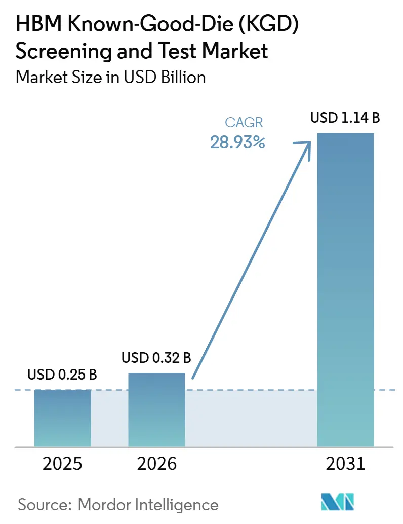
The HBM Known-Good-Die (KGD) Screening and Test Market size is expected to increase from USD 0.25 billion in 2025 to USD 0.32 billion in 2026 and reach USD 1.14 billion by 2031, growing at a CAGR of 28.93% over 2026-2031. The HBM known-good-die (KGD) screening and test market is expanding because HBM stacks now sit at the center of AI accelerator design, which raises the cost of every defect that escapes early screening. Test intensity is also rising as stack heights increase, and the number of validation points increases across die, stack, package, and final integration flows. The shift to logic-foundry base dies in HBM4 is changing the validation path and is bringing more foundries and packaging participants into the HBM Known-Good-Die (KGD) Screening and Test Market. Suppliers are responding with a mix of memory testers, probe solutions, burn-in systems, and handling upgrades, which is widening the equipment opportunity beyond a narrow tester-only cycle. The strongest opportunities remain tied to pre-stack screening, stacked-die validation, wafer-level burn-in, and service-based test capacity that help customers manage fast production ramps without carrying all capacity in-house.
Key Report Takeaways
- By test stage, wafer-level testing held 44.13% of HBM known-good-die (KGD) screening and test market share in 2025, while stacked-die testing is projected to expand at a 29.67% CAGR through 2031.
- By tester type, memory testers held 38.23% share in 2025, while burn-in systems are projected to expand at a 29.58% CAGR through 2031.
- By HBM generation, HBM3E held 58.46% share in 2025, while HBM4 is projected to expand at a 29.51% CAGR through 2031.
- By test technology, conventional electrical testing held 75.42% share in 2025, while wafer-level burn-in is projected to expand at a 29.62% CAGR through 2031.
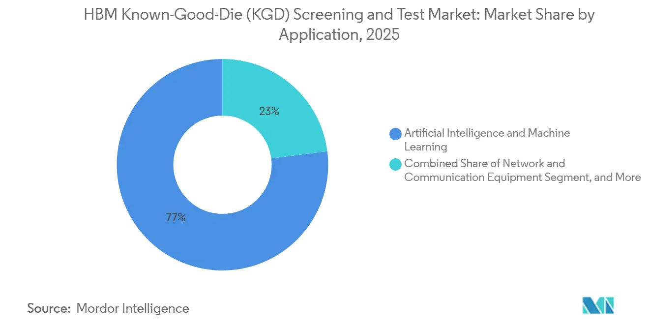
- By application, AI and machine learning held 77.04% share of the HBM known-good-die (KGD) screening and test market in 2025, and it is also projected to expand at a 29.83% CAGR through 2031.
- By end-use industry, memory manufacturers held 63.24% share in 2025, while foundries are projected to expand at a 29.54% CAGR through 2031.
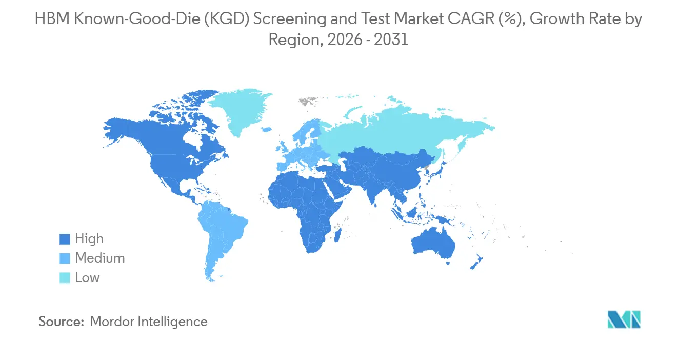
- By geography, Asia-Pacific held 83.49% share in 2025, while it is also projected to expand at a 29.78% CAGR through 2031.
Note: Market size and forecast figures in this report are generated using Mordor Intelligence’s proprietary estimation framework, updated with the latest available data and insights as of January 2026.
Market Trends and Insights
Drivers Impact Analysis of HBM Known-Good-Die (KGD) Screening and Test Market*
| Driver | (~) % Impact on CAGR Forecast | Geographic Relevance | Impact Timeline |
|---|---|---|---|
| Rising AI Accelerator Demand Increasing KGD Screening Intensity | +8.2% | Global, with primary concentration in Asia-Pacific, South Korea, Taiwan, and North America | Short term (≤ 2 years) |
| Shift-Left Test Strategies to Protect Multi-Die Yield | +5.6% | Asia-Pacific core, South Korea and Taiwan, with spillover to North America OSAT and IDM facilities | Medium term (2-4 years) |
| Higher HBM Stack Heights Raising Defect Containment Needs | +4.3% | South Korea, Taiwan, Japan, with secondary impact in North America and Europe | Medium term (2-4 years) |
| Growing Use of Wafer-Level Burn-In for Latent Defect Removal | +3.8% | Global, with strongest uptake in Asia-Pacific and early adoption in North America | Medium term (2-4 years) |
| Tight Signal Integrity and Current Requirements Expanding Test Content | +2.9% | Global, particularly relevant in North America and Europe | Long term (≥ 4 years) |
| HBM4 Qualification Complexity Increasing Pre-Stack Validation Spend | +2.4% | Asia-Pacific, South Korea, Japan, and Taiwan | Short term (≤ 2 years) |
| Source: Mordor Intelligence | |||
Rising AI Accelerator Demand Increasing KGD Screening Intensity
The HBM known-good-die (KGD) screening and test market is moving higher because AI accelerators now rely on HBM as a core performance building block rather than an optional memory upgrade. That shift raises the penalty for any die or stack failure, because defects can disrupt a much more expensive compute module rather than a stand-alone memory component. FormFactor stated in 2026 that AI and HBM are changing semiconductor test priorities by pushing more attention toward early defect removal, yield stability, and package-level cost protection.[1] The same pressure is evident in how customers qualify devices, as stronger screening has become part of the commercial requirements for high-value AI hardware rather than a back-end quality preference. As AI server deployments widen, the HBM known-good-die (KGD) screening and test market is benefiting from both higher unit demand and more screening steps per device. This keeps test demand elevated even when wafer output growth alone does not fully explain the pace of equipment and capacity additions.
Shift-Left Test Strategies to Protect Multi-Die Yield
The HBM known-good-die (KGD) screening and test market is also being shaped by a clear move toward earlier screening points in the production flow. FormFactor noted in May 2026 that early test strategies are critical because they determine whether manufactured dies enter stacking as proven-qualified material, which protects downstream yield and costs. That logic becomes stronger as stacks move from fewer layers to 12- and 16-high designs, because a single weak die can compromise a much larger portion of the assembled value. Siemens EDA showed in April 2026 that HBM4 changes the test program architecture by shifting the base die toward a logic-foundry approach, making validation continuity across die, stack, and package stages more important. In practice, this means the HBM known-good-die (KGD) screening and test market is no longer centered solely on pass-or-fail screening at a single point in the line. It is increasingly organized around a sequence of protection gates that try to keep scrap from compounding as integration value rises.
Higher HBM Stack Heights Raising Defect Containment Needs
The HBM known-good-die (KGD) screening and test market is being lifted by the simple fact that taller stacks are harder to validate and more expensive to fail. JEDEC’s HBM4 standard formalized support for configurations ranging from 4-high to 16-high, demonstrating how far vertical complexity has already advanced in the current cycle. Siemens EDA also highlighted that HBM3E and HBM4 designs carry more demanding interface and architecture requirements, which broaden the scope of what must be checked before final integration. As a result, the HBM known-good-die (KGD) screening and test market is seeing more value shift toward stacked-die validation, thermal awareness during test, and known-good-stack discipline. FormFactor’s 2026 commentary reinforced that each additional layer makes early accuracy more valuable because downstream assembly consumes more otherwise usable material if one die fails. The result is not just longer programs, but a broader need for defect containment before advanced packaging locks in more cost.
Growing Use of Wafer-Level Burn-In for Latent Defect Removal
Wafer-level burn-in is becoming a more visible growth engine in the HBM known-good-die (KGD) screening and test market, as customers seek to remove latent defects before expensive package assembly begins. Aehr Test Systems announced in August 2025 that a leading AI processor supplier ordered a wafer-level burn-in and functional test evaluation program that used a custom high-power 300 mm contactor designed to deliver hundreds of amperes of current. That announcement matters because it shows burn-in moving from a limited reliability step toward an earlier production screen for AI-class devices. JEDEC’s April 2025 HBM4 standard also raised the performance bar for future HBM validation, which supports broader interest in stronger pre-package screening methods. The HBM known-good-die (KGD) screening and test market is therefore gaining a service and equipment layer around burn-in that did not carry the same urgency in older memory cycles. Customers who are unsure about near-term demand can also use external burn-in capacity first, which lowers the barrier to adoption while still increasing test intensity.
Restraints Impact Analysis of HBM Known-Good-Die (KGD) Screening and Test Market*
| Restraint | (~) % Impact on CAGR Forecast | Geographic Relevance | Impact Timeline |
|---|---|---|---|
| High Cost of Advanced ATE and Probe Infrastructure | -3.6% | Global, most acute for OSAT and smaller IDMs in South Korea, China, and Southeast Asia | Short term (≤ 2 years) |
| Limited Throughput at High Parallelism Levels | -2.3% | Global, particularly in Asia-Pacific production hubs | Medium term (2-4 years) |
| Thermal and Power Delivery Constraints During Full-Rate Testing | -1.8% | Asia-Pacific and North America | Medium term (2-4 years) |
| Yield Loss Risk from Over-Screening and False Rejects | -1.1% | Global, especially where stress parameters are not tightly calibrated | Long term (≥ 4 years) |
| Source: Mordor Intelligence | |||
High Cost of Advanced ATE and Probe Infrastructure
The HBM known-good-die (KGD) screening and test market still faces a meaningful barrier because advanced memory test, probing, and handling systems are expensive to qualify and difficult to deploy at scale. Advantest’s December 2025 launch of the M5241 Memory Handler, with support for up to 512 parallel test sites and throughput up to 46,000 units per hour, shows how specialized the latest infrastructure has become. Aehr’s August 2025 evaluation order also showed that new programs can require custom contactor design and unusually high current delivery, which adds another layer of development effort beyond standard test insertion. Technoprobe’s 2025 Capital Market Day presentation further underscored the need for vertically integrated MEMS capabilities in advanced probe environments, suggesting that supply depth matters as much as simple equipment ownership. These conditions favor large memory manufacturers and well-qualified partners that can spread engineering costs across high volumes. Smaller participants can still enter the HBM known-good-die (KGD) screening and test market, but they often do so through narrower roles or service models rather than full in-house platform builds.
Limited Throughput at High Parallelism Levels
The HBM known-good-die (KGD) screening and test market also has to work around a practical throughput limit, because higher parallelism does not remove all mechanical, thermal, and contact constraints. Advantest’s M5241 specification shows that the industry is pushing hard on parallel test capacity, yet the need for new sockets, handling precision, and stable device contact makes these gains difficult to scale without supporting changes elsewhere in the flow. This is one reason customers continue to value service access and staged deployment, since peak screening demand can arrive faster than internal throughput can be built. Aehr’s service-oriented positioning around evaluation and burn-in access reflects the need for flexible capacity during qualification ramps. The constraint is especially relevant when production schedules move quickly, but validation time cannot be compressed at the same pace. Even with strong demand, the HBM known-good-die (KGD) screening and test market can only add capacity as fast as equipment, contact technology, and stable handling performance allow.
*Our forecasts treat driver/restraint impacts as directional, not additive. The impact forecasts reflect baseline growth, mix effects, and variable interactions.
HBM Known-Good-Die (KGD) Screening and Test Market Segment Analysis
By Test Stage:
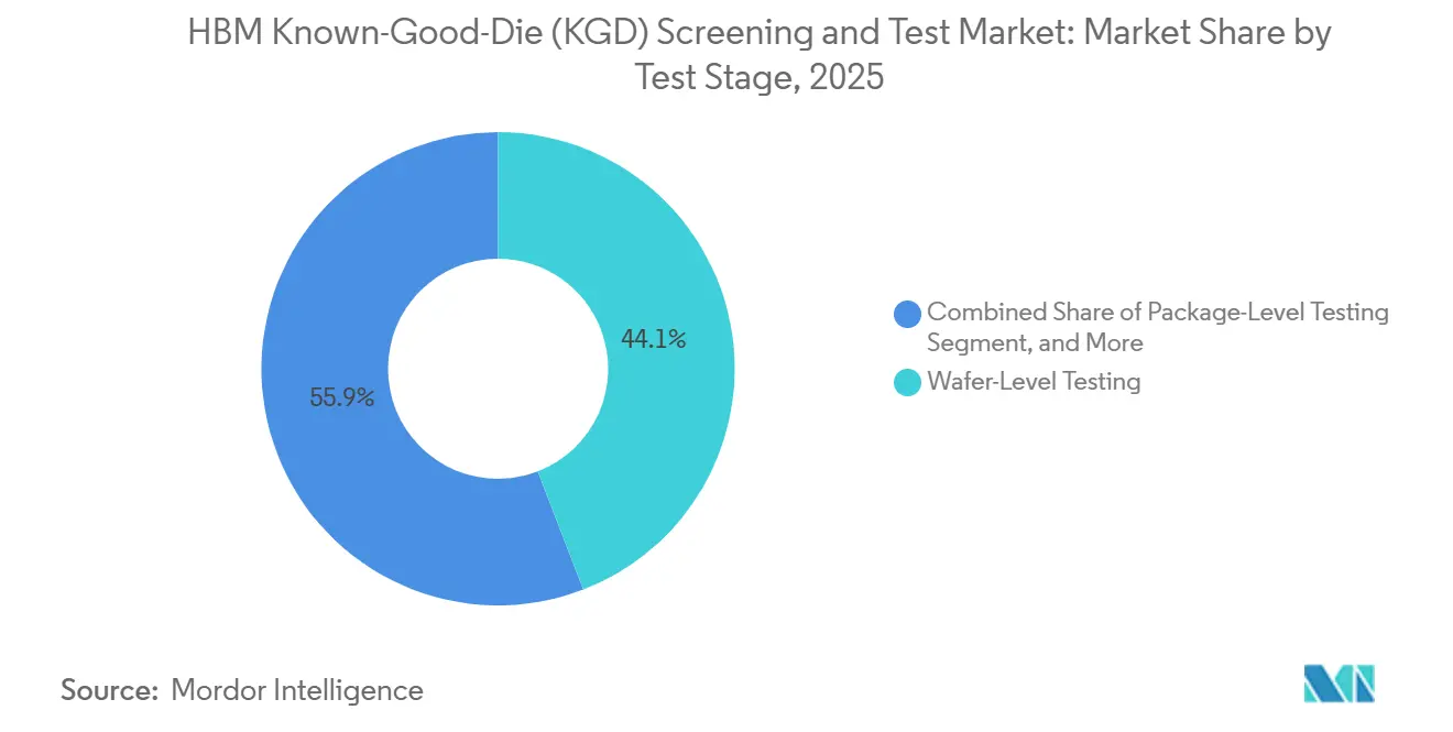
Wafer-Level Testing Anchors Early Defect EconomicsWafer-level testing held the largest share among test-stage segments at 44.13% in 2025, making it the first economic control point in the HBM known-good-die (KGD) screening and test market. That lead reflects the simple cost logic of the flow, since defects caught before stacking prevent more expensive material from moving into later process steps. FormFactor stated in 2026 that early screening determines whether manufactured dies reach stacking as qualified material, which gives wafer-level testing a direct role in downstream yield stability. In the HBM known-good-die (KGD) screening and test market, wafer-level decisions shape not only yield but also the capital, handling time, and package assembly effort committed to each future stack. This is why the segment remained the anchor stage even as validation demands broadened beyond the wafer.
The rest of the test-stage mix is still expanding because later validation points cannot be removed from advanced HBM programs. Package-level and system-level work remain relevant as HBM4 introduces a logic-foundry base die and a more complex integration path that wafer screening alone cannot fully cover. Stacked-die testing is the fastest-growing segment, with a 29.67% CAGR through 2031, underscoring the growing value of known-good-stack verification before final package assembly. The need grows as stack height increases and as customers seek more confidence before devices enter CoWoS and other advanced packaging flows. JEDEC’s HBM4 framework supports this direction by formalizing more demanding stack configurations, which naturally widens the role of intermediate validation gates.[2] For the HBM known-good-die (KGD) screening and test market, the stage mix is therefore widening around a clear idea, early screens save money, but later screens protect the much larger value created by stacking and integration.

By Tester Type:
Burn-In Systems Close in on the Established Memory Tester LeadMemory testers were the largest tester type segment in 2025, with a 38.23% share, supported by their roles across wafer test, functional screening, and qualification cycles spanning multiple HBM generations. Their lead comes from broad installed use and the fact that conventional memory testing remains central to day-to-day production decisions in the HBM known-good-die (KGD) screening and testing market. Advantest’s product activity in late 2025 showed how vendors continue to strengthen this base, especially for high-performance AI memory devices that need higher parallelism and steadier throughput. Memory testers also remain relevant because each new HBM generation still requires a substantial body of electrical characterization and production-qualified test content. That keeps the segment firmly embedded in the HBM known-good-die (KGD) screening and test market even as newer methods gain ground.
Burn-in systems are the fastest-growing tester type, with a 29.58% CAGR through 2031, reflecting the shift toward earlier removal of latent defects in expensive AI and HBM devices. Aehr’s 2025 evaluation order showed that customers are willing to test new wafer-level burn-in paths when the cost of downstream failure becomes too high to ignore. Burn-in is no longer treated only as a late reliability step, because in the HBM known-good-die (KGD) screening and test market it increasingly acts as a protection gate before advanced packaging locks in more value. Probe cards and wafer probe systems remain essential around this trend, since stronger screening still depends on accurate contact, stable current delivery, and repeatable mechanical performance. Technoprobe’s 2025 expansion plans underline that suppliers also see a durable opportunity in the contact layer that supports these rising test loads. The result is a tester landscape where memory testers still lead today, but burn-in systems are closing the gap because their role is moving closer to the center of production economics.
By HBM Generation:
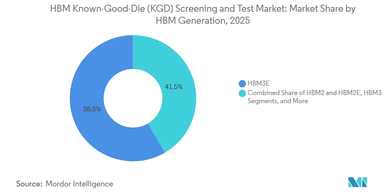
HBM3E Anchors Current Revenue as HBM4 Reshapes Validation StandardsHBM3E accounted for 58.46% of generation-specific revenue in 2025, making it the primary revenue anchor for the HBM known-good-die (KGD) screening and test market. That position matched its role in the active ramp of AI accelerator platforms during the year. HBM3E also carried a heavier test burden than older generations because its stack depth and interface demands were already high enough to require more careful screening and yield control. In the HBM known-good-die (KGD) screening and test market, HBM3E therefore marked the point at which test intensity shifted from an advanced requirement to a routine condition of participation. It set the current operating baseline for how suppliers organize equipment, program development, and qualification discipline.
HBM4 is the fastest-growing generation segment, with a 29.51% CAGR through 2031, and its rise is closely tied to changes in both architecture and validation methods. JEDEC published the HBM4 standard in April 2025, covering 4-high to 16-high stack options, 24 Gb and 32 Gb die densities, and up to 64 GB cube density. Siemens EDA then described in April 2026 how the move toward a logic-foundry base die changes the test program architecture for HBM4 and raises the need for full-flow validation continuity. Older generations such as HBM2 and HBM2E are still present, but their test spend is fading as production shifts toward newer devices. HBM3 remains in the mix, though it now sits between a still-dominant HBM3E base and a faster-rising HBM4 pipeline. For the HBM known-good-die (KGD) screening and test market, that makes HBM4 less of a simple generational upgrade and more of a reset in how future validation standards are defined.
By Test Technology:
Conventional Testing Maintains Dominance Under Mounting PressureConventional electrical testing accounted for 75.42% of test technology revenue in 2025, keeping it far ahead of alternative methods in the HBM known-good-die (KGD) screening and test market. Its lead came from installed infrastructure, qualified programs, and the fact that electrical screening remains the foundation of normal production release. This segment also benefits from process familiarity, since customers trust long-established flows when yield learning is still underway in new HBM ramps. Even so, the HBM known-good-die (KGD) screening and test market is showing clear signs that conventional testing alone is no longer enough for the highest-value devices. The leadership of this segment is real, but it is increasingly being defended rather than extended.
Wafer-level burn-in is the fastest-growing test technology, with a 29.62% CAGR through 2031, reflecting rising demand for latent defect removal before advanced packaging. Aehr’s 2025 evaluation program showed that the method is now being adapted for high-power AI device screening at the wafer stage, with a custom contact design built around heavy current delivery. Built-in self-test-based screening is also becoming increasingly relevant in HBM4, as the logic-foundry base die enables more advanced program architecture and interface-speed validation. JEDEC’s HBM4 framework supports that direction by formalizing the next level of bandwidth, capacity, and stack complexity that future screening must address. Advanced probe and metrology-assisted methods remain smaller, but they are gaining relevance where fine pitch, current density, and post-bond verification need more specialized tools. This leaves the HBM known-good-die (KGD) screening and test market with a technology mix that is still led by conventional flows but increasingly supplemented by methods designed for tougher failure modes.
By Application:
AI and Machine Learning Holds Commanding Share with No Near-Term ChallengerAI and machine learning accounted for 77.04% of total application revenue in 2025, giving this segment the largest share of the HBM known-good-die (KGD) screening and testing market. Its scale reflects the near-central role of HBM in top-tier accelerators, where bandwidth density and package efficiency directly shape system value. In the HBM known-good-die (KGD) screening and test market, this makes AI not just the largest use case, but the application that most strongly changes how customers think about screening depth and defect risk. FormFactor’s 2026 commentary on AI and HBM test priorities supports that shift, especially around early screening, yield protection, and package-level cost control. The same application is also the fastest-growing, with a 29.83% CAGR through 2031, indicating the segment that already dominates current demand is widening its lead.
Other application segments remain relevant, but none carry the same urgency or economic weight. High-performance computing continues to support demand for large compute programs that require documented memory reliability and repeatable validation. Gaming and graphics, network and communication equipment, and automotive and transportation all remain smaller and more price-sensitive within the HBM known-good-die (KGD) screening and test market. These segments benefit from stronger test capability once it exists, but they do not drive the same pace of capital decisions as AI deployments do. Their demand is therefore more selective and less able to justify the highest-cost screening paths on its own. This leaves AI and machine learning with a commanding position that still shapes both current revenue and the direction of future tool investment.
By End-Use Industry:
Memory Manufacturers Dominate as Foundries Capture Incremental ShareMemory manufacturers accounted for 63.24% of end-use industry revenue in 2025, giving them the leading position in the HBM known-good-die (KGD) screening and testing market. That result aligns with the business structure because HBM qualification begins with companies that design, fabricate, and release the memory stacks themselves. These players typically run integrated screening environments where design teams and test teams work closely around new ramps and yield learning. The HBM known-good-die (KGD) screening and test market, therefore, remains anchored in the internal validation systems of the largest memory suppliers. Their share also reflects the fact that they undertake the earliest and most intensive qualification work before other participants assume a broader operational role.
Foundries are the fastest-growing end-use segment at a 29.54% CAGR through 2031, and that acceleration follows the structural shift introduced by HBM4. Siemens EDA explained that HBM4 changes the architecture path by moving the base die into a logic foundry environment, which pulls foundries deeper into the validation chain. As a result, the HBM known-good-die (KGD) screening and test market is no longer confined to memory fabrication alone, because foundries are now closer to the point where package integration risk is managed. IDMs and OSATs remain smaller in revenue share, but they still matter as supporting capacity holders and process partners during busy qualification periods. Their role is especially important when customers need overflow test support or package-adjacent validation that memory manufacturers do not keep fully in-house. This is why the end-use mix is evolving from a memory-led structure toward a wider chain that includes more foundry influence without displacing memory manufacturers from the center.
Geography Analysis
APAC HBM Known-Good-Die (KGD) Screening and Test Market
Asia-Pacific commanded 83.49% of revenue in 2025, giving it the largest share of the HBM known-good-die (KGD) screening and testing market, and it is also the fastest-growing regional segment at a 29.78% CAGR through 2031. The region leads because HBM production, test equipment supply, and advanced packaging capacity are all concentrated there. South Korea remains the main anchor, since the leading HBM manufacturers drive most of the early qualification work and much of the demand for advanced screening systems. Taiwan plays a critical integration role through its foundry and packaging capacity, making its test infrastructure part of the wider HBM release path. Japan is strengthening its regional base through memory test, probe, and metrology capabilities, while China is still building local HBM test capacity from an earlier position on the qualification curve.
Japan and APAC HBM Known-Good-Die (KGD) Screening and Test Market
Asia-Pacific also benefits from policy support and equipment depth that reinforce its long-term position in the HBM known-good-die (KGD) screening and test market. Japan’s semiconductor-related capital investment program totaled JPY 4.5 trillion (USD 30.1 billion) under the regular budget and JPY 6.3 trillion (USD 42.1 billion) under supplementary allocations as of December 2025. That spending environment helps sustain demand for test equipment, probe technology, and process capability across the regional supply chain. The HBM known-good-die (KGD) screening and test market is therefore not only concentrated in Asia-Pacific by production share, but also supported there by the deepest combination of manufacturing, integration, and supplier readiness. This creates a structural advantage that other regions are unlikely to close quickly.
The Americas and EMEA HBM Known-Good-Die (KGD) Screening and Test Market
North America held a smaller share in 2025, but it remains strategically important because hyperscaler demand and test program ownership influence how the HBM known-good-die (KGD) screening and test market evolves. The region is home to major equipment and solution providers, and it also shapes qualification requirements through the buying power of AI infrastructure customers. Aehr’s wafer-level burn-in activity in California shows that North America can influence early-stage screening methods even without matching Asia-Pacific in direct HBM wafer output.[3] Europe and South America remain smaller, though Europe keeps a meaningful role through probe and metrology specialists such as Technoprobe, while the Middle East and Africa are still early-stage participants whose relevance is linked more to downstream AI system demand than to upstream HBM screening capacity.
Competitive Landscape
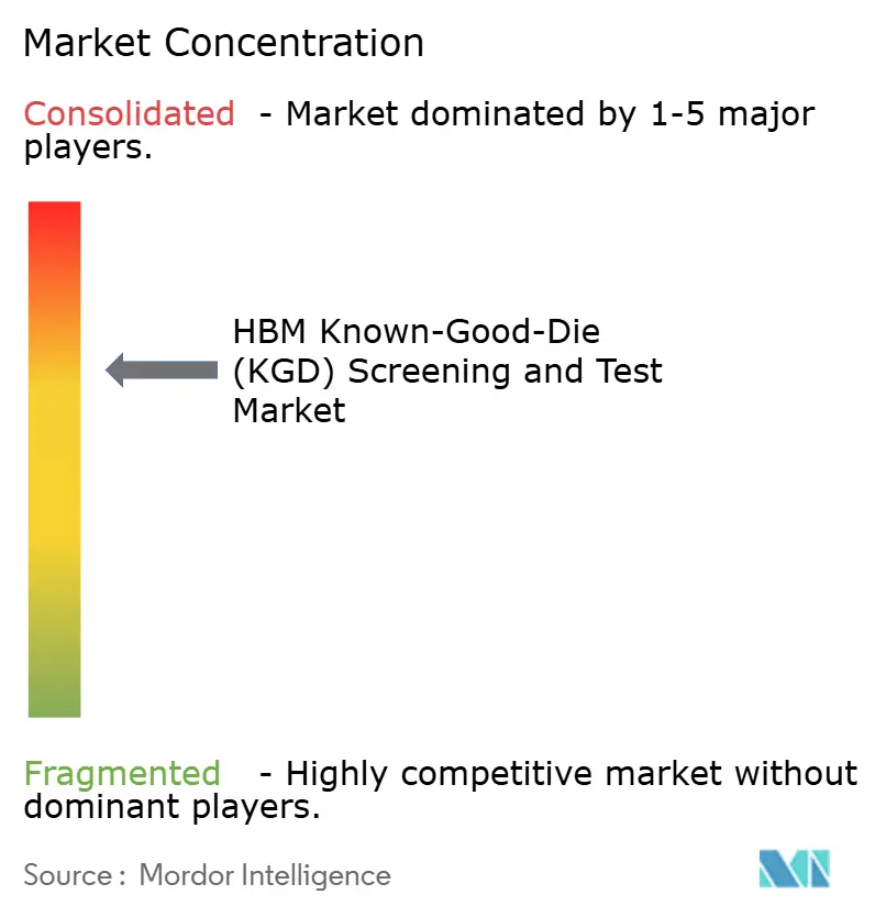
The HBM known-good-die (KGD) screening and test market is moderately concentrated at the tester level and more distributed across probe cards, handlers, and burn-in platforms. Advantest and Teradyne together accounted for over 90% of ATE revenue in the input material, underscoring how strongly qualified tester relationships shape the market. At the same time, the broader HBM known-good-die (KGD) screening and test market includes narrower specialists that compete in contact technology, burn-in, inspection, and handling, so concentration is lower once the full workflow is considered. This creates a structure where scale matters most in core ATE, while focused engineering depth matters more in surrounding sub-systems. Customers, therefore, tend to manage a mix of entrenched lead suppliers and smaller specialists rather than depend on a single vendor across the entire chain.
Strategic moves during 2025 and 2026 show how suppliers are positioning for the next phase of demand. Advantest introduced the M5241 Memory Handler in December 2025 with support for up to 512 parallel test sites, a move that directly addressed the throughput and parallelism demands of high-performance AI memory devices. Aehr Test Systems received a wafer-level burn-in evaluation order in August 2025 that highlighted customer interest in earlier high-power screening for AI-related devices. Technoprobe used its April 2025 Capital Market Day to outline expansion plans for HBM-related probe card opportunities, which signaled that the contact layer is becoming a more strategic part of the HBM known-good-die (KGD) screening and test market. These moves point to a market where leaders are adding scale, while specialists are defending position through process-specific capability.
Competition is also shaped by technical lock-in rather than price alone. Siemens EDA showed that HBM4 changes design and test architecture, which means qualified program knowledge will continue to act as a strong barrier to entry in the HBM known-good-die (KGD) screening and test market.[4] The strongest white space remains in wafer-level burn-in services, fine-pitch probe solutions, and automation that can handle taller stacks without reducing yield discipline. JEDEC standards guide much of the technical compliance path, but real competitive advantage still comes from who can meet those requirements consistently in production. That is why the HBM known-good-die (KGD) screening and test market remains intense, even though only a few players dominate the core tester layer.
HBM Known-Good-Die (KGD) Screening and Test Industry Leaders
-
Teradyne Inc.
-
Advantest Corporation
-
FormFactor, Inc.
-
Cohu, Inc.
-
Keysight Technologies, Inc.
- *Disclaimer: Major Players sorted in no particular order
HBM Known-Good-Die (KGD) Screening and Test Market Companies Covered in this Report
- Teradyne Inc.
- Advantest Corporation
- FormFactor, Inc.
- Cohu, Inc.
- Keysight Technologies, Inc.
- TECHWING INC.
- DI Corporation
- Shenzhen SEICHI Technologies Co., Ltd.
- Wuhan Jingce Electronic Group Co., Ltd.
- Suzhou Secote Precision Electronic Co., Ltd.
- Chroma ATE Inc.
- SPEA S.p.A.
- Tokyo Electron Limited
- Onto Innovation Inc.
- Kulicke and Soffa Industries, Inc.
- ASMPT Limited
Recent Industry Developments in HBM Known-Good-Die (KGD) Screening and Test Market
- July 2026: Samsung Electronics confirmed its HBM4E reliability test yield exceeded 70%, signaling that development had entered a stable phase ahead of planned customer sample shipments. Samsung had initiated first HBM4E sample shipments in May 2026, targeting NVIDIA's Vera Rubin Ultra accelerator platform for 2027.
- June 2026: Teradyne and Tokyo Electron Limited jointly commercialized an integrated KGD screening test cell for AI and data center devices, combining Teradyne's UltraFLEXplus test platform with TEL's Prexa SDP singulated device prober. The system targeted foundries, fabless designers, and OSATs requiring device screening at multiple points in an advanced packaging flow.
- June 2026: TECHWING received its first Cube Prober HBM inspection equipment order from SK Hynix following customer quality certification in March 2026. This added SK Hynix to TECHWING's existing Samsung supply relationship and positioned the company for Micron evaluation currently underway.
- December 2025: Advantest introduced the M5241 Memory Handler, supporting up to 512 parallel test sites and a maximum throughput of 46,000 units per hour, covering DDR5, next-generation DRAM, NAND, and AI memory applications. First shipments were scheduled for Q2 2026, with multiple major memory manufacturers already preparing for adoption.
Global HBM Known-Good-Die (KGD) Screening and Test Market Report Scope
The HBM Known-Good-Die (KGD) Screening and Test Market covers the processes, equipment, and services used to verify the functionality, reliability, and performance of high-bandwidth memory dies before integration into advanced semiconductor packages. The market scope includes wafer-level testing, die-level screening, burn-in testing, electrical testing, reliability assessment, and quality validation for HBM applications across data centers, artificial intelligence, high-performance computing, graphics processing, and other advanced electronics.
The HBM Known-Good-Die (KGD) Screening and Test Market report is segmented by Test Stage (Wafer-Level Testing, Stacked-Die Testing, Package-Level Testing, and System-Level Testing), Tester Type (Memory Tester, Wafer Probe Systems, Probe Cards, and Burn-In Systems), HBM Generation (HBM2 and HBM2E, HBM3, HBM3E, and HBM4), Test Technology (Conventional Electrical Testing, Built-In Self-Test Based Screening, Wafer-Level Burn-In, and Advanced Probe and Metrology-Assisted Test), Application (Artificial Intelligence and Machine Learning, High-Performance Computing, Gaming and Graphics Processing, Network and Communication Equipment, and Automotive and Transportation), End-Use Industry (Memory Manufacturers, Integrated Device Manufacturers [IDMs], Foundries, and Outsourced Semiconductor Assembly and Test [OSAT]), and Geography (North America, Europe, Asia-Pacific, South America, and Middle East and Africa). The Market Forecasts are Provided in Terms of Value (USD).
Segmentation Overview
| Wafer-Level Testing |
| Stacked-Die Testing |
| Package-Level Testing |
| System-Level Testing |
| Memory Tester |
| Wafer Probe Systems |
| Probe Cards |
| Burn-In Systems |
| HBM2 and HBM2E |
| HBM3 |
| HBM3E |
| HBM4 |
| Conventional Electrical Testing |
| Built-In Self-Test Based Screening |
| Wafer-Level Burn-In |
| Advanced Probe and Metrology-Assisted Test |
| Artificial Intelligence and Machine Learning |
| High-Performance Computing |
| Gaming and Graphics Processing |
| Network and Communication Equipment |
| Automotive and Transportation |
| Memory Manufacturers |
| Integrated Device Manufacturers (IDMs) |
| Foundries |
| Outsourced Semiconductor Assembly and Test (OSAT) |
| North America | United States |
| Canada | |
| Mexico | |
| Europe | Germany |
| United Kingdom | |
| France | |
| Italy | |
| Rest of Europe | |
| Asia-Pacific | China |
| Japan | |
| South Korea | |
| Taiwan | |
| India | |
| Rest of Asia-Pacific | |
| South America | |
| Middle East and Africa |
| By Test Stage | Wafer-Level Testing | |
| Stacked-Die Testing | ||
| Package-Level Testing | ||
| System-Level Testing | ||
| By Tester Type | Memory Tester | |
| Wafer Probe Systems | ||
| Probe Cards | ||
| Burn-In Systems | ||
| By HBM Generation | HBM2 and HBM2E | |
| HBM3 | ||
| HBM3E | ||
| HBM4 | ||
| By Test Technology | Conventional Electrical Testing | |
| Built-In Self-Test Based Screening | ||
| Wafer-Level Burn-In | ||
| Advanced Probe and Metrology-Assisted Test | ||
| By Application | Artificial Intelligence and Machine Learning | |
| High-Performance Computing | ||
| Gaming and Graphics Processing | ||
| Network and Communication Equipment | ||
| Automotive and Transportation | ||
| By End-Use Industry | Memory Manufacturers | |
| Integrated Device Manufacturers (IDMs) | ||
| Foundries | ||
| Outsourced Semiconductor Assembly and Test (OSAT) | ||
| By Geography | North America | United States |
| Canada | ||
| Mexico | ||
| Europe | Germany | |
| United Kingdom | ||
| France | ||
| Italy | ||
| Rest of Europe | ||
| Asia-Pacific | China | |
| Japan | ||
| South Korea | ||
| Taiwan | ||
| India | ||
| Rest of Asia-Pacific | ||
| South America | ||
| Middle East and Africa | ||
Key Questions Answered in the Report
What is the 2026 size of the HBM known-good-die (KGD) screening and test market, and how large will it be by 2031?
The HBM known-good-die (KGD) screening and test market stood at USD 0.32 billion in 2026 and is forecast to reach USD 1.14 billion by 2031 at a 28.93% CAGR.
Which test stage leads current revenue in HBM KGD screening and test?
Wafer-level testing led with a 44.13% share in 2025 because it is the earliest point where defects can be removed before stacking adds more cost.
Why is stacked-die testing growing so quickly?
Stacked-die testing is projected to grow at a 29.67% CAGR because taller HBM stacks raise the cost of a single defect and increase the need for known-good-stack validation.
Which tester category is expanding the fastest?
Burn-in systems are the fastest-growing tester type, with a 29.58% CAGR through 2031, as customers push latent defect screening earlier in the flow.
Why does Asia-Pacific dominate this space?
Asia-Pacific held 83.49% share in 2025 and is also the fastest-growing region at 29.78% CAGR because it combines HBM production, foundry and packaging capacity, and key test equipment suppliers.
Which application drives most demand for HBM KGD screening and test?
AI and machine learning accounted for 77.04% of revenue in 2025 and is also the fastest-growing application at a 29.83% CAGR, reflecting the central role of HBM in advanced AI accelerators.