Glass Wafer Carrier Market Size and Share
Market Overview
| Study Period | 2019 - 2030 |
|---|---|
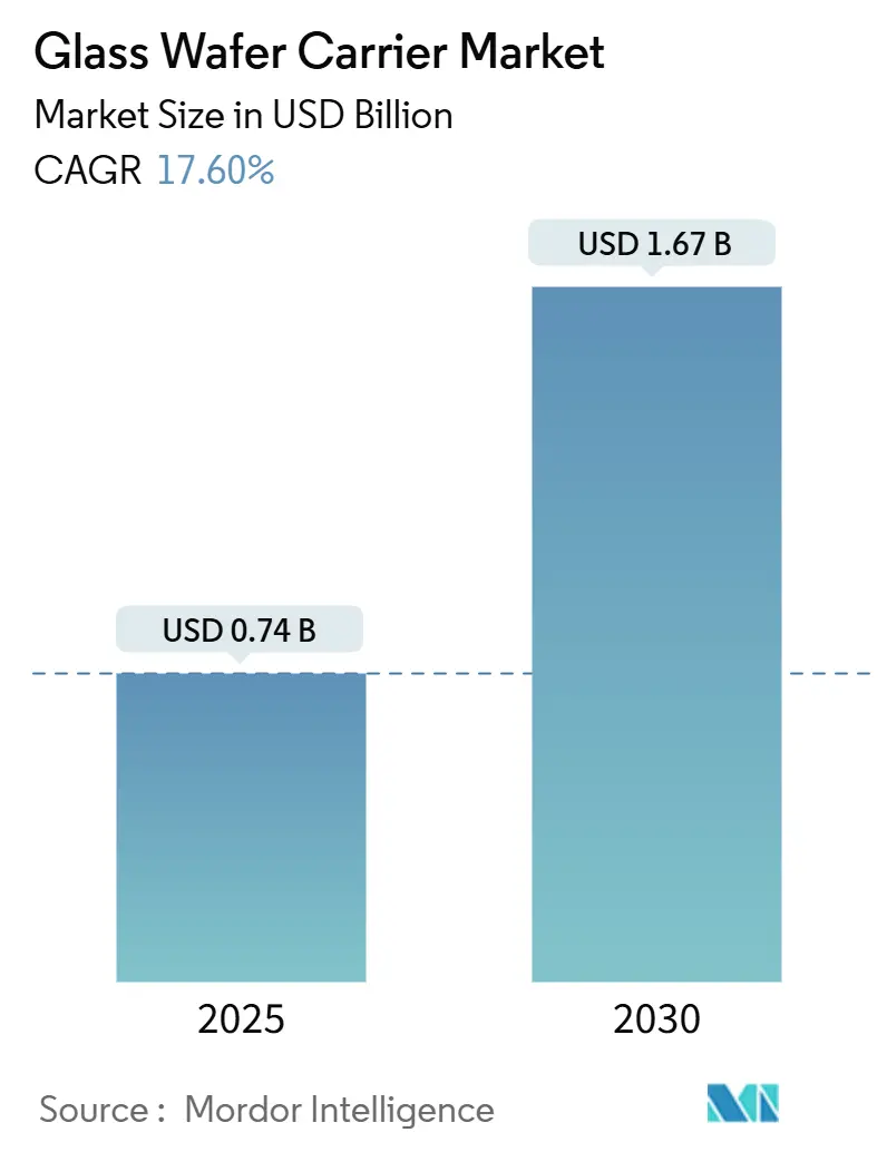
| Market Size (2025) | USD 0.74 Billion |
| Market Size (2030) | USD 1.67 Billion |
| Growth Rate (2025 - 2030) | 17.60% CAGR |
| Fastest Growing Market | Asia Pacific |
| Largest Market | Asia Pacific |
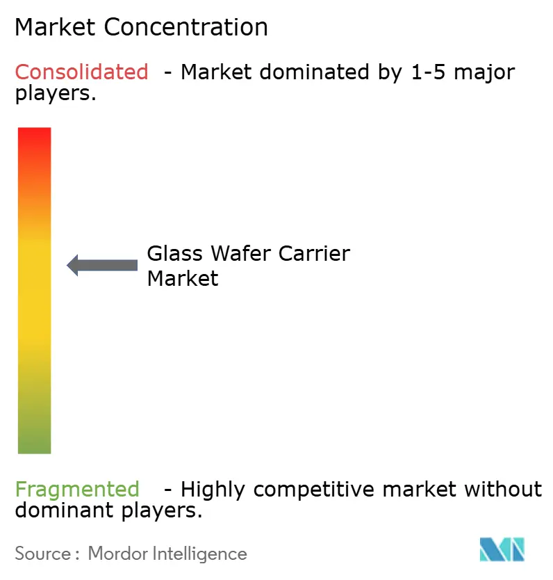
| Market Concentration | Medium |
Major Players *Disclaimer: Major Players sorted in no particular order Image © Mordor Intelligence. Reuse requires attribution under CC BY 4.0. | |
Glass Wafer Carrier Market Analysis by Mordor Intelligence
The Glass Wafer Carrier market size is estimated at USD 0.74 billion in 2025 and is projected to reach USD 1.67 billion by 2030, representing a robust 17.6% CAGR over the forecast period. Three converging trends drive demand growth: the faster adoption of fan-out wafer-level packaging, rising throughput for ultra-thin wafers with thicknesses below 50 µm, and the early migration to 650 × 650 mm panel-level packaging for AI accelerators. Advanced fabs now specify borosilicate or fused-silica carriers to minimize warpage while maintaining dimensional stability through high-temperature cycles. In parallel, the CHIPS Act triggers domestic investments that tighten supply chains and stimulate localized glass substrate production. Supply-chain bottlenecks affecting float-glass feedstock and the mechanical brittleness of large-format carriers remain key challenges, pressuring manufacturers to refine formulations and automation techniques that guard yields without inflating cost structures.
Key Report Takeaways
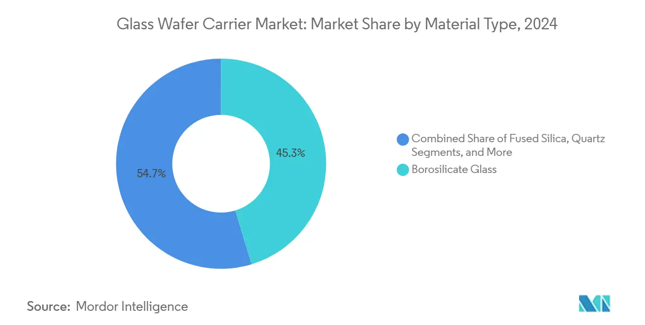
- By material, borosilicate captured 45.3% of the Glass Wafer Carrier market share in 2024, while fused silica is projected to expand at a 19.1% CAGR to 2030.
- By wafer size, the 300 mm segment accounted for 66.7% of the Glass Wafer Carrier market size in 2024 and is projected to advance at a 19.3% CAGR through 2030.
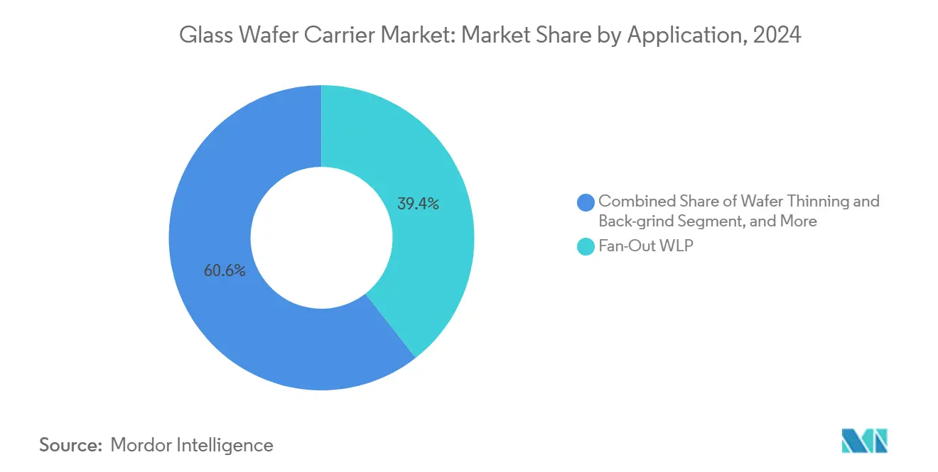
- By application, the fan-out wafer-level packaging segment accounted for 39.4% of the Glass Wafer Carrier market size in 2024, while panel-level packaging is projected to advance at an 18.4% CAGR through 2030.
- By end-user, foundries and IDMs segment accounted for 44.1% of the Glass Wafer Carrier market size in 2024, while OSATs are projected to advance at an 18.5% CAGR through 2030.
- By geography, the Asia-Pacific region dominated the Glass Wafer Carrier market, accounting for a 56.9% share of the market size in 2024. North America is poised for the fastest growth, at 18.2% CAGR through 2030.
Note: Market size and forecast figures in this report are generated using Mordor Intelligence’s proprietary estimation framework, updated with the latest available data and insights as of January 2026.
Global Glass Wafer Carrier Market Trends and Insights
Drivers Impact Analysis*
| Driver | (~) % Impact on CAGR Forecast | Geographic Relevance | Impact Timeline |
|---|---|---|---|
| Surging adoption of fan-out wafer-level packaging | +4.20% | Global, APAC lead | Medium term (2-4 years) |
| Boom in ultra-thin wafer demand for 3D-IC/HBM stacks | +3.80% | APAC core, North America spill-over | Long term (≥ 4 years) |
| Expansion of 300 mm fab capacity across East Asia | +3.10% | East Asia primary | Medium term (2-4 years) |
| Rapid shift toward photonic and xenon-flash debond flows | +2.70% | Global early adoption | Short term (≤ 2 years) |
| CHIPS-Act-backed U.S. glass-substrate additions | +2.40% | North America | Long term (≥ 4 years) |
| Emergence of 650 × 650 mm glass panel-level packaging | +1.40% | AI manufacturing hubs | Long term (≥ 4 years) |
| Source: Mordor Intelligence | |||
Surging Adoption of Fan-Out Wafer-Level Packaging
Fan-out wafer-level packaging volumes increased by 34% in 2024, elevating glass carriers from specialty to production-line status. These carriers supply the rigidity needed to protect dies thinned to 25 µm, while enabling multilayer redistribution at tight line widths. Mobile processors, automotive radar, and edge-AI devices now require flatter surfaces and improved thermal performance, which are not available on organic substrates. TSMC’s shift toward glass panel-level solutions signals a broader industry endorsement likely to propagate within two years.[1]Source: Mark LaPedus, “Glass Substrates Gain Momentum In Advanced Packaging,” SEMIENGINEERING.COM
Boom in Ultra-Thin Wafer Demand for 3D-IC/HBM Stacks
High-bandwidth memory output surged 67% in 2024 as tier-one memory makers pursued stack heights beyond 16 layers. Thinning wafers to 30 µm requires near-perfect support; glass excels with a thermal expansion deviation of less than 0.5 ppm/°C, ensuring TSV alignment remains intact during grind-back, laser drilling, and Cu-fill sequences. NEG’s GC Core™ glass, ground to 0.1 µm flatness, exemplifies this precision.
Expansion of 300 mm Fab Capacity Across East Asia
East Asia invested USD 47 billion in 300 mm fab projects in 2024, resulting in a 2.25× increase in carrier surface area compared to the 200 mm node. TSMC’s Arizona plant and Samsung’s Pyeongtaek lines allocate dedicated glass-handling tracks. Local suppliers in Japan and South Korea are now scaling production, trimming cycle times, and reducing freight risk.[2]SEMI, “Global Fab Forecast 2024–2027,” SEMI.ORG
Rapid Shift Toward Photonic and Xenon-Flash Debond Flows
Photonic debonding volumes almost doubled in 2024 as compound semiconductors migrated away from thermal release layers. UV-transparent fused silica carriers transmit 365 nm energy cleanly, cutting adhesion without heat-induced warpage. Resonac’s xenon-flash platforms already achieve sub-10-second cycles, opening cost-out pathways for MEMS and PIC fabs.
Restraints Impact Analysis*
| Restraint | (~) % Impact on CAGR Forecast | Geographic Relevance | Impact Timeline |
|---|---|---|---|
| High precision-glass cost and capital intensity | -2.80% | Global | Medium term (2-4 years) |
| Carrier breakage and yield-loss from brittleness | -2.10% | Panel-level lines | Short term (≤ 2 years) |
| Silicon carrier + IR nanocleaving substitute | -1.70% | North America, Europe | Medium term (2-4 years) |
| Float-glass supply crunch from solar-PV pull | -1.40% | Global, varying by region | Short term (≤ 2 years) |
| Source: Mordor Intelligence | |||
High Precision-Glass Cost and Capital-Intensive Production
Precision glass commands a premium, priced three to five times above silicon equivalents. Equipment for ultra-flat grinding, double-side polishing, and interferometric metrology swallows up to 70% of a greenfield plant’s capital budget. Margins tightened in 2024 as Plan Optik disclosed revenue compression linked to inventory corrections and competitive quotes.[3]Plan Optik AG, “FY 2024 Earnings Presentation,” PLANOPTIK.COM
Carrier Breakage and Yield Loss from Brittleness
Large-panel carriers fracture at rates near 4%, dwarfing silicon’s sub-0.1% breakage. Stress arises in automated transport and thermal excursions. ASE Technology installed low-vibration vacuum chucks yet still reports edge-chip incidents on 500 µm slabs. Enhanced edge beveling and chemical strengthening help, but material physics restrain headway.[4]ASE Technology Holding, “Annual Report 2024,” ASEGLOBAL.COM
*Our forecasts treat driver/restraint impacts as directional, not additive. The impact forecasts reflect baseline growth, mix effects, and variable interactions.
Segment Analysis
By Material Type: Fused Silica Gains on Thermal Performance
The Glass Wafer Carrier market size for borosilicate glass reached USD 0.34 billion in 2024, equal to a 45.3% share. Stable expansion continues, as its thermal expansion parallels that of silicon, resulting in substrate bow during RDL cure steps. Fused silica, meanwhile, accelerates at a 19.1% CAGR, underpinned by photonic debond flows and high-heat HBM production. Quartz serves as a niche MEMS dielectric, where zero alkali and outgassing are not a concern. Alumino-borosilicate enters as a reinforced alternative that absorbs mechanical stress better than standard borosilicate. Regional bias persists: East-Asian fabs prioritize borosilicate for cost, whereas U.S. pilots lean on fused silica for UV tasks.
Second-generation suppliers promote hybrid stacks, thin alumino-borosilicate faces laminated onto low-CTE cores, to strike a balance between cost and toughness. While price deltas narrow within high-value packaging lines, commodity segments continue to gravitate toward traditional borosilicate. Competitive thrust centers on securing float-glass feedstock and raising polishing yields above 95%. Environmental goals also play a role as fused-silica processing consumes more energy; sustainability audits may tip the selection in mass-production scenarios.


By Wafer Size: 300 mm Segment Holds Commanding Lead
In 2024, the 300 mm class generated two-thirds of the Glass Wafer Carrier market share, USD 0.49 billion, lifted by frontline logic and memory nodes. Capital deployments in Taiwan, South Korea, and Arizona amplify throughput, driving steady double-digit growth. Equipment ecosystems favor this geometry, providing vendors with scale economies that lower the per-unit cost and shorten lead times. At the same time, 200 mm remains entrenched for legacy MEMS and SiC power dies, where 300 mm tools would under-utilize throughput.
Road-mapping for 450 mm stagnates, as economics tilt instead to panel-level formats that combine multiple 300 mm equivalents on glass plates. Suppliers thus funnel R&D into maintaining surface planarity across 300 mm even after repeated reuse cycles. Service contracts for reclaiming scratched carriers extend the life of the carriers and curb scrap. A marginal uptick in 150 mm persists in certain industrial sensors, yet its revenue contribution stays minor.
By Application: Panel-Level Packaging Becomes Fastest Riser
The Glass Wafer Carrier market share for fan-out WLP was 39.4% in 2024, as mobile SoC vendors value low-profile footprints. However, panel-level packaging rockets forward at 18.4% CAGR, taking advantage of 650 × 650 mm plates that cut die-cost per area for AI accelerators. Through-glass-via interposers follow, blending electrical isolation with dimensional precision for RF and optical modules. Wafer thinning/back-grind remains foundational, with carriers reused across several cycles, tightening total-cost metrics.
Synergies arise when a single carrier type passes through sequential steps, thinning, TSV formation, RDL, and final singulation, resulting in lower changeover downtime. Vendors respond by formulating adhesive layers compatible with multi-pass thermal histories. Thermal budgets shrink to protect fine-pitch Cu redistribution; glass offers superior heat flux, simplifying modeling for equipment integrators.
By End-User Industry: OSATs Accelerate
Foundries and IDMs held 44.1% Glass Wafer Carrier market share in 2024, capitalizing on integrated control over front-to-back-end flows. OSATs, though, exhibit the swiftest climb at an 18.5% CAGR as customer outsourcing moves beyond wire-bond lines toward advanced packages. To stand apart, leading OSATs retrofit lines with specialized photonic debond chambers and low-stress handling robots sized for 600 mm carriers.
Research institutes and pilot fabs still claim a predictable tranche of orders, especially for exploratory compositions like fluorine-doped silica. Specialty MEMS/photonics houses request custom shapes and drilled vias, forcing vendors to diversify product catalogs. Co-development pacts, therefore, grow vital, linking glass makers, adhesive formulators, and tool OEMs into closed-loop feedback structures that drive down ramp time.
Geography Analysis
The Asia-Pacific region generated 56.9% of the Glass Wafer Carrier market revenue in 2024 and is projected to compound at a 18.2% growth rate through 2030. China’s subsidy-backed fabs add capacity while Taiwan’s TSMC evaluates glass panel carriers for future FO-PLP builds. South Korea’s Samsung and SK Hynix channel budgets into ultrathin HBM lines, each necessitating high-rigidity fused-silica plates. Japan sustains its upstream strength through NEG and AGC, ensuring local access to float-glass feedstock and polishing expertise.
North America ranks second, fueled by USD 52 billion in CHIPS-Act allocations that target reshoring. Corning secured USD 32 million to pilot UV-transparent carriers, and Absolics captured USD 75 million for a North Carolina plant, with completion due by 2027. Intel’s commitment to glass substrates for high-performance compute signals a domestic pull that could reroute part of the Asia-bound supply. Government-backed grants also accelerate equipment uptake, cutting lead times for precision grinders and metrology kits.
Europe delivers stable demand, anchored in the automotive and industrial electronics sectors. Plan Optik’s facility upgrade in Hungary introduces a 650 mm plate capability, enabling EU OSATs to sample panel-level packaging before full-scale adoption. Germany’s Tier-1 auto suppliers are pushing MEMS braking sensors that prefer quartz carriers for their purity. Regulatory emphasis on supply resilience encourages in-region partnerships, though currency swings and energy costs influence site economics.


Competitive Landscape
Competition remains moderate, with the top five firms accounting for roughly 40% of the Glass Wafer Carrier market share. SCHOTT, Corning, and AGC leverage multi-industry glass portfolios to spread capital costs, while Plan Optik, Tecnisco, and NEG focus on semiconductor-grade precision. Innovation hotbeds involve UV-transparent fused-silica blends, stress-relief edge finishing, and in-situ thickness metrology embedded on carrier frames.
Collaborations bridge material vendors with tool makers: LPKF’s Vitrion platform integrates glass milling and bonding, allowing fabs to insource carrier prep and debonding in one cell. This vertical integration could pressure standalone substrate suppliers unless they bolster service, reclaim, or logistics offerings. Meanwhile, traditional silicon carrier providers pilot IR nanocleave options that could cannibalize entry-level glass volumes within three years.
Strategic investments underscore scale economics. SCHOTT consolidated its semiconductor unit with USD 150 million earmarked for doubling capacity in Germany and Singapore. Samsung frames a USD 2.3 billion consortium to assure 650 mm plate supply by 2026. Corning’s U.S. grant underwrites a pilot line, positioning it to ramp once customers lock high-volume purchase orders. Intellectual-property filings spike around composite glass layers and adhesive chemistries that enable faster photonic release, hinting at new licensing revenue beyond direct carrier sales.
Glass Wafer Carrier Industry Leaders
SCHOTT AG
Corning Incorporated
AGC Inc.
Nippon Electric Glass Co., Ltd.
Plan Optik AG
- *Disclaimer: Major Players sorted in no particular order

Recent Industry Developments
- January 2025: Samsung Electronics unveiled a USD 2.3 billion alliance with multiple glass-substrate partners to reach 650 × 650 mm mass production by 2026.
- January 2025: LPKF Laser & Electronics expanded Vitrion systems with integrated glass handling for semiconductor fabs.
- December 2024: SCHOTT AG created a dedicated semiconductor division and budgeted USD 150 million for precision glass tools across Germany and Singapore.
- December 2024: Swift Glass Company launched custom small-volume wafer fabrication services for R&D groups.


Global Glass Wafer Carrier Market Report Scope
| Borosilicate Glass |
| Fused Silica |
| Quartz |
| Alumino-Borosilicate |
| 150 mm |
| 200 mm |
| 300 mm |
| 450 mm (Road-map) |
| Wafer Thinning and Back-grind |
| Fan-Out WLP |
| Through-Glass-Via (TGV) Interposers |
| Panel-Level Packaging |
| Foundries and IDMs |
| OSATs |
| Research and Development / Pilot Lines |
| Specialty MEMS and Photonics Fabs |
| North America | United States |
| Canada | |
| Mexico | |
| South America | Brazil |
| Argentina | |
| Rest of South America | |
| Europe | Germany |
| United Kingdom | |
| France | |
| Italy | |
| Rest of Europe | |
| Asia-Pacific | China |
| Japan | |
| South Korea | |
| India | |
| Rest of Asia-Pacific | |
| Middle East | Saudi Arabia |
| United Arab Emirates | |
| Rest of Middle East | |
| Africa | South Africa |
| Rest of Africa |
| By Material Type | Borosilicate Glass | |
| Fused Silica | ||
| Quartz | ||
| Alumino-Borosilicate | ||
| By Wafer Size | 150 mm | |
| 200 mm | ||
| 300 mm | ||
| 450 mm (Road-map) | ||
| By Application | Wafer Thinning and Back-grind | |
| Fan-Out WLP | ||
| Through-Glass-Via (TGV) Interposers | ||
| Panel-Level Packaging | ||
| By End-User Industry | Foundries and IDMs | |
| OSATs | ||
| Research and Development / Pilot Lines | ||
| Specialty MEMS and Photonics Fabs | ||
| By Geography | North America | United States |
| Canada | ||
| Mexico | ||
| South America | Brazil | |
| Argentina | ||
| Rest of South America | ||
| Europe | Germany | |
| United Kingdom | ||
| France | ||
| Italy | ||
| Rest of Europe | ||
| Asia-Pacific | China | |
| Japan | ||
| South Korea | ||
| India | ||
| Rest of Asia-Pacific | ||
| Middle East | Saudi Arabia | |
| United Arab Emirates | ||
| Rest of Middle East | ||
| Africa | South Africa | |
| Rest of Africa | ||


Key Questions Answered in the Report
What value does the Glass Wafer Carrier market reach by 2030?
Forecasts place the market at USD 1.67 billion by 2030 under a 17.6% CAGR.
Which wafer size currently dominates carrier demand?
The 300 mm class accounts for 66.7% of demand and grows the quickest on sustained fab expansion.
Why are fused-silica carriers gaining traction?
Their UV transparency and low CTE suit photonic debonding and ultra-thin HBM stack processing.
Which region leads consumption today?
Asia-Pacific commands 56.9% share, anchored by Chinese, Taiwanese, and South Korean fabs.
How does panel-level packaging influence future demand?
AI accelerators require 650 × 650 mm plates, making panel-level packaging the fastest-rising application at an 18.4% CAGR.
What is the main supply-chain hurdle?
Float-glass shortages, intensified by solar-PV demand, constrain feedstock and inflate lead times.
Page last updated on:


