GaN-on-Silicon (GaN-on-Si) LED Epitaxial Wafer Market Size and Share
Market Overview
| Study Period | 2020 - 2031 |
|---|---|
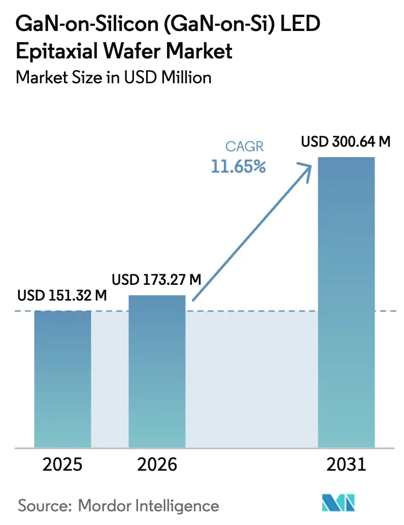
| Market Size (2026) | USD 173.27 Million |
| Market Size (2031) | USD 300.64 Million |
| Growth Rate (2026 - 2031) | 11.65% CAGR |
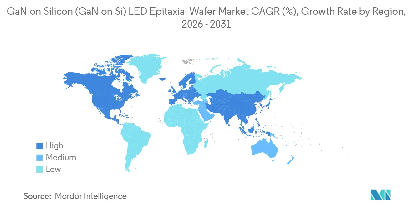
| Fastest Growing Market | Asia Pacific |
| Largest Market | Asia Pacific |
| Market Concentration | Medium |
Major Players *Disclaimer: Major Players sorted in no particular order Image © Mordor Intelligence. Reuse requires attribution under CC BY 4.0. | |
GaN-on-Silicon (GaN-on-Si) LED Epitaxial Wafer Market Analysis by Mordor Intelligence
The GaN-on-Silicon LED epitaxial wafer market size is expected to increase from USD 0.151 billion in 2025 to USD 0.173 billion in 2026 and reach USD 0.301 billion by 2031, growing at a CAGR of 11.65% over 2026-2031. Persistent regulatory pressure on lamp efficacy, the migration to 200 mm processing, and micro-LED adoption in augmented-reality (AR) devices are converging to widen the commercial appeal of GaN-on-Si epitaxy. Across lighting classes, LED penetration has already made incandescent and halogen formats economically obsolete, yet tightening standards in the United States, the European Union, China, and India are expanding the addressable market for more efficient die architectures. Foundries view the compatibility of silicon substrates with existing CMOS lines as a capital-saving lever, spurring vendors to pilot 300 mm MOCVD tools that can deliver nine times the die output of 100 mm sapphire runs. Momentum is reinforced by vertically integrated display programs targeting sub-10 µm pixels, where GaN-on-Si eliminates the wafer-to-driver bonding step that sapphire requires. Competitive dynamics remain moderate because roughly fifteen players control reactor capacity and hold the process know-how needed to keep defect densities within acceptable limits.
Key Report Takeaways
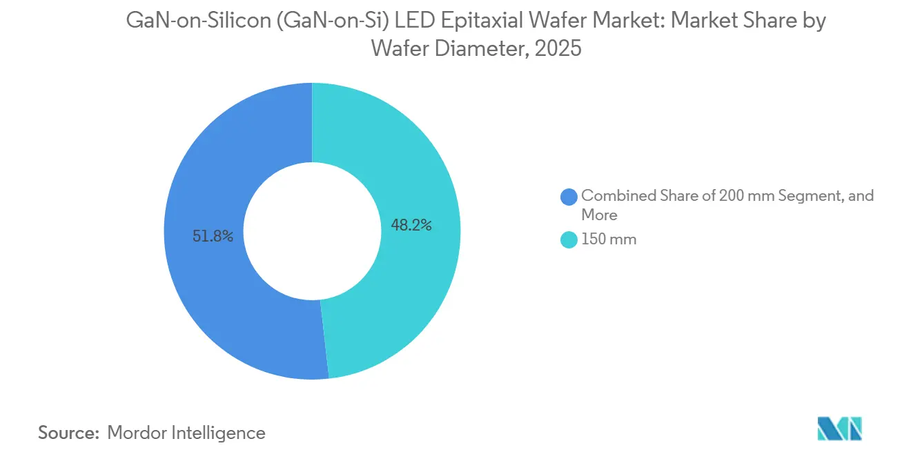
- By wafer diameter, the 150 mm format held 48.19% of the GaN-on-Silicon LED epitaxial wafer market share in 2025, while 200 mm wafers are projected to expand at a 12.48% CAGR through 2031.
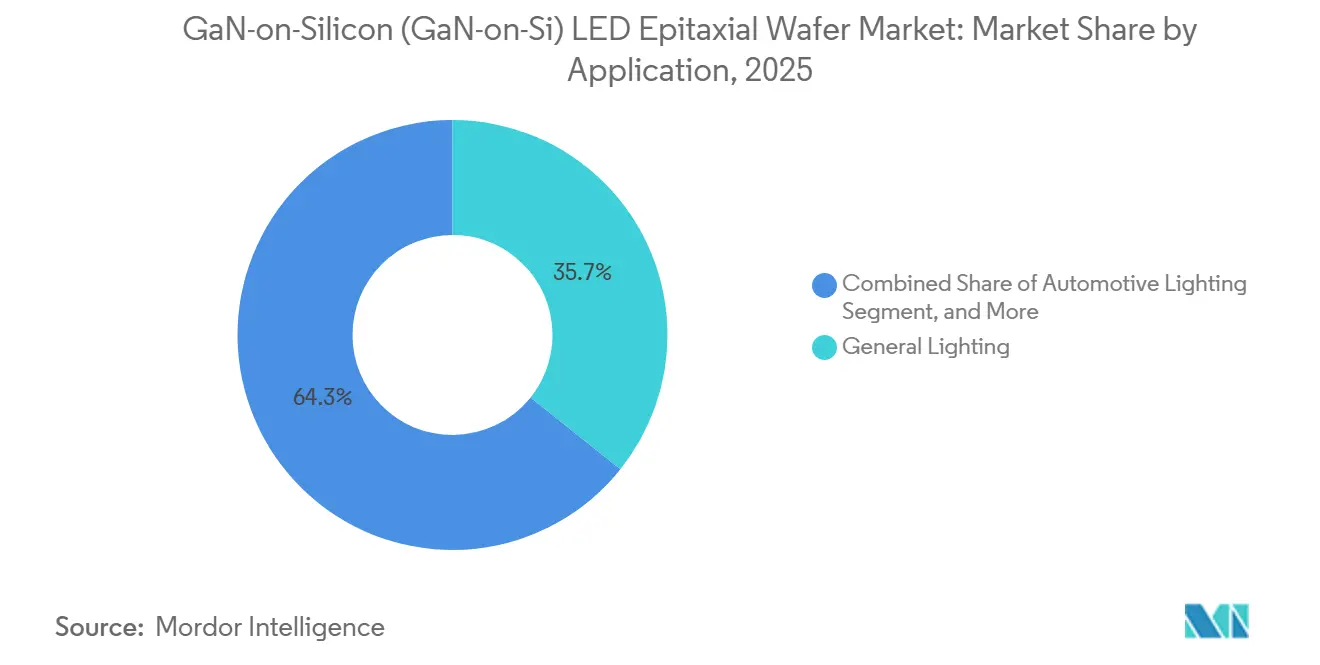
- By application, general lighting commanded 35.73% of 2025 revenue, whereas display and backlighting are forecast to accelerate at a 12.97% CAGR over 2026-2031.
- By geography, Asia-Pacific maintained 66.93% share of 2025 sales and is expected to grow at a 12.64% CAGR to 2031.
Note: Market size and forecast figures in this report are generated using Mordor Intelligence’s proprietary estimation framework, updated with the latest available data and insights as of January 2026.
Global GaN-on-Silicon (GaN-on-Si) LED Epitaxial Wafer Market Trends and Insights
Drivers Impact Analysis*
| Driver | (~) % Impact on CAGR Forecast | Geographic Relevance | Impact Timeline |
|---|---|---|---|
| Increasing Demand for Energy-Efficient Solid-State Lighting | +2.8% | Global, stronger in North America and the EU | Medium term (2-4 years) |
| Cost Reduction Potential of GaN-on-Si Substrates Versus Sapphire | +2.5% | Asia-Pacific core, spill-over to North America and the EU | Short term (≤ 2 years) |
| Expansion of 200 mm and 300 mm CMOS Fabs for GaN-on-Si Epi | +2.2% | Asia-Pacific (China, Taiwan, South Korea), North America | Medium term (2-4 years) |
| Growth of Automotive LED Adoption for Headlamps and ADAS Sensors | +1.8% | Global, with early gains in the EU and China | Long term (≥ 4 years) |
| Government Regulations Phasing-Out Incandescent and Halogen Bulbs | +1.5% | North America, EU, China, India | Short term (≤ 2 years) |
| Integration of GaN-Based Micro-LED Arrays for AR Displays | +1.2% | Asia-Pacific (China, South Korea), North America | Long term (≥ 4 years) |
| Source: Mordor Intelligence | |||
Increasing Demand for Energy-Efficient Solid-State Lighting
Solid-state lighting accounted for 65% of installed luminaires in 2025, yet the International Energy Agency calculated in 2026 that another 30% efficiency gain remains technically achievable, leaving ample headroom for the GaN-on-Silicon LED epitaxial wafer market to grow. The U.S. Department of Energy rule, effective July 2028, mandates lamp efficacies that cannot be met by incandescent or halogen technology, explicitly citing alternative substrate options, including silicon, as viable design pathways.[1]U.S. Department of Energy, “Energy Conservation Standards for General Service Lamps,” Federal Register, energy.gov Fixture makers addressing residential and commercial retrofits now face dual pressures to lower bill-of-materials cost and exceed 130 lm/W efficacy thresholds, and larger-diameter silicon wafers reduce per-lumen cost by up to 25% compared with 100 mm sapphire. Utility rebate programs in North America reinforce demand by linking incentives to high-efficacy product listings. Collectively, these forces sustain a multiyear pull for GaN-on-Si epitaxy across high-volume lighting classes.
Cost Reduction Potential of GaN-on-Si Substrates Versus Sapphire
Silicon substrates sell for USD 50-70 per 200 mm wafer, roughly one-eighth the price of comparable sapphire, creating a structural advantage that expands as diameters scale upward. Demonstrations in 2025 showed that 5.25 × 10⁸ cm⁻² dislocation densities are now routine, cutting the efficiency gap with sapphire while still preserving a 70% substrate-cost delta. In reactor economics, a 200 mm GaN-on-Si run produces four times the die area of a 100 mm sapphire load, enabling a single tool to support 500,000 onboard-charger LEDs yearly, according to a Shanghai materials supplier. Such scale profitability, however, hinges on maintaining yields above 85%, a target achievable only with real-time warp control and optimized buffer stacks. As these process refinements diffuse, silicon’s price advantage is expected to offset residual efficiency penalties in cost-sensitive end markets.
Expansion of 200 mm and 300 mm CMOS Fabs for GaN-on-Si Epi
Veeco shipped 300 mm GaN-on-Si MOCVD pilot tools in 2026, targeting volume production the following year and signaling that mainstream semiconductor equipment vendors now consider the technology ready for high-throughput adoption.[2]Veeco Instruments Inc., “Veeco Announces 300 mm GaN-on-Si MOCVD Reactor Evaluation,” veeco.com Foundry alliances are multiplying: onsemi and GlobalFoundries disclosed a 200 mm collaboration with engineering samples slated for H1 2026, while Infineon sent 300 mm GaN wafers to customers in Q4 2025 and added more than 40 GaN devices to its catalog. Compatibility reduces upfront capital by up to 40% compared with greenfield sapphire lines, as existing photolithography, implant, and metrology tools can be reused. Display makers benefit most, as a 300 mm GaN-on-Si wafer can yield 1.2 million 5 µm micro-LEDs, enough for 15–20 AR modules, boosting the substrate’s strategic importance in next-generation wearables.
Growth of Automotive LED Adoption for Headlamps and ADAS Sensors
LED headlamps exceeded 50% penetration in global vehicle production during 2025, partly because European regulations now require adaptive driving beam capability. ams OSRAM’s OSLON Compact RM, introduced in November 2025, highlights demand for matrix-beam devices that bundle multiple emitters at high luminance.[3]ams OSRAM, “OSLON Compact RM LED for Automotive Headlamps,” osram.com GaN-on-Si enables monolithic RGB options that simplify supply chains for full-color ADAS modules, and a leading Chinese manufacturer reported achieving 22% external quantum efficiency for red emitters on silicon, a milestone once thought impractical. Automotive qualification remains lengthy, often 24 months, but design wins booked in 2025-2026 are scheduled to hit volume by 2028. In electric vehicles, where lighting draws on the traction battery, the 30-40% power savings over halogen options further amplifies OEM interest in GaN-on-Si die.
Restraints Impact Analysis*
| Restraint | (~) % Impact on CAGR Forecast | Geographic Relevance | Impact Timeline |
|---|---|---|---|
| High Dislocation Density and Yield Challenges in GaN-on-Si Epitaxy | −1.8% | Global, acute in North America and the EU | Short term (≤ 2 years) |
| Competition from Sapphire-Based LED Wafers | −1.5% | Global, strongest pressure in Asia-Pacific | Medium term (2-4 years) |
| Limited Availability of Patterned Si Substrates with Stress Control | −0.8% | Asia-Pacific and North America | Medium term (2-4 years) |
| Risk of IP Litigation in GaN Epitaxy Processes | −0.6% | Global, higher exposure in North America and the EU | Long term (≥ 4 years) |
| Source: Mordor Intelligence | |||
High Dislocation Density and Yield Challenges in GaN-on-Si Epitaxy
The 17% lattice mismatch between silicon and gallium nitride drives threading dislocation densities near 1 × 10⁹ cm⁻², roughly two orders of magnitude higher than sapphire-based material and a primary cause of 10-15% lower external quantum efficiency. Buffer techniques such as 60-pair AlN/GaN multilayers can suppress stress but add up to USD 12 per wafer in extra reactor time.[4]Journal of Materials Science, “Optimal AlN/GaN Multilayer Buffer Design,” springer.com Warp above 100 µm on 200 mm substrates complicates lithography and dicing, forcing some fabs to scrap edge die, which undermines the cost benefits of larger wafers. Progress is uneven: while a handful of suppliers now report sub-30 µm bow metrics, the lack of standardized processes keeps average yields below the 90% benchmark enjoyed by sapphire competitors.
Competition from Sapphire-Based LED Wafers
Sapphire continues to deliver dislocation densities below 1 × 10⁸ cm⁻² and supports external quantum efficiencies above 80% for blue LEDs, benchmarks that uphold its position in premium lighting, horticultural, and UV niches. Patterned sapphire substrates, which boost light extraction by up to 20%, are widely available and inexpensive to integrate. Leading sapphire suppliers invested in new 150 mm and 200 mm lines during 2025, betting that their performance edge will persist even as silicon closes the cost gap. For applications where lumen maintenance and chromatic stability trump first-cost economics, such as automotive headlamps, medical lighting, and cinema projection, sapphire’s entrenched ecosystem remains difficult to displace.
*Our forecasts treat driver/restraint impacts as directional, not additive. The impact forecasts reflect baseline growth, mix effects, and variable interactions.
Segment Analysis
By Wafer Diameter: Shift Toward 200 mm and 300 mm Platforms
The 200 mm tier, representing the bridge between legacy 150 mm and emerging 300 mm production, is expanding faster than the overall GaN-on-Silicon LED epitaxial wafer market. In 2025 the 150 mm format still dominated shipments at 48.19%, thanks to its entrenched position in mid-power illumination and backlighting, yet equipment roadmaps now overwhelmingly favor larger diameters. Volume evaluations of 300 mm reactors in 2026 underscore a strategic pivot to 12-inch tools that yield ninefold more die than 100 mm sapphire lots, an arithmetic that resonates strongly with display panel makers. The GaN-on-Silicon LED epitaxial wafer market size advantage grows as wafer area increases, but only if edge exclusion and crack-related scrap remain minimal. Suppliers claiming sub-30 µm bow on 8-inch substrates report yields north of 90%, demonstrating that process control rather than raw diameter dictates economic viability.
Capital allocation is following the same logic. Foundries with depreciated 200 mm CMOS lines can retrofit chambers for GaN-on-Si at roughly 60% of the cost of new sapphire fabs, a figure that appeals to investors wary of cyclical LED margins. Although 100 mm and 150 mm wafers will persist in UV and prototyping roles, analysts expect new capacity additions after 2027 to skew heavily toward 200 mm and above. The inflection to 300 mm still confronts technical hurdles, most notably uniform gas flow and temperature gradients, but the payback, especially for high-pixel-count displays, is compelling enough that several tier-one equipment makers have committed to shipping production systems by 2027.


By Application: Displays Outpace Lighting Growth
General lighting retained a 35.73% revenue share in 2025, mirroring its role as the broadest volume outlet for LEDs, yet growth now tilts toward display and backlighting, projected to rise at 12.97% CAGR. AR eyewear, smart-watches, and automotive head-up displays all demand sub-10 µm micro-LEDs, a geometry better served by monolithic GaN-on-Si processing than by pick-and-place assembly from sapphire dice. Ennostar and Allos highlighted this transition in January 2026 when they agreed to co-develop 8-inch wafers that integrate epitaxy with CMOS driver circuits, thereby eliminating the costly mass-transfer step.
The GaN-on-Silicon LED epitaxial wafer market size allocated to automotive lighting is climbing on the back of adaptive beam headlights and energy-efficient daytime running lights, both of which value on-chip RGB integration. Specialty categories, UV curing, horticulture, and sterilization, remain niche but high margin, and suppliers continue to evaluate whether silicon substrates can meet their stringent wavelength and power density requirements. For now, sapphire maintains a stronghold in these domains, though hybrid wafer approaches and buffer innovations may widen GaN-on-Si’s addressable range before the end of the forecast horizon.
Geography Analysis
Asia-Pacific is both the manufacturing and innovation engine of the GaN-on-Silicon LED epitaxial wafer market. The region accounted for 66.93% of 2025 revenue, and national programs in China, Taiwan, and South Korea are forecast to drive a 12.64% CAGR through 2031. China alone has earmarked RMB 80 billion (USD 11.2 billion) for micro-LED infrastructure, much of which is dedicated to 200 mm and 300 mm GaN-on-Si fabs, ensuring local availability of large-diameter substrates. Taiwanese and Japanese vendors complement this scale with materials science expertise and equipment innovation. Nichia’s mercury-free UV initiative and ROHM’s decision to internalize GaN processes underscore a trend toward captive supply chains.
North America concentrates on high-value applications and policy-led adoption. The Department of Energy ruling that becomes enforceable in July 2028 virtually guarantees replacement of legacy incandescent stock, whereas partnerships such as onsemi-GlobalFoundries signal a willingness to incorporate GaN epitaxy into brownfield CMOS lines. European participation is anchored by Germany’s Infineon, whose 300 mm wafer deliveries in Q4 2025 position the region as a node for automotive and industrial power devices. While South America, the Middle East, and Africa currently absorb only single-digit percentages of global shipments, off-grid solar lighting initiatives and industrial modernization efforts are likely to generate incremental demand for low-cost GaN-on-Si LEDs by the end of the decade.
Asia-Pacific’s dominance is enhanced by vertical integration: Chinese and Taiwanese firms increasingly handle everything from raw GaN growth to finished LED modules, compressing the supply chain and accelerating time-to-market. Government subsidies lower risk for pilot lines, allowing experimentation with 300 mm formats that Western competitors regard as capital intensive. Nonetheless, intellectual-property enforcement challenges and export-control uncertainties temper the region’s longer-term outlook, encouraging multinational OEMs to adopt dual-sourcing strategies that include North American or European epitaxial capacity.

Competitive Landscape
The GaN-on-Silicon LED epitaxial wafer market features a mid-level concentration profile, with roughly fifteen vertically integrated suppliers controlling most reactor capacity worldwide. Incumbents such as Nichia, Epistar, and Samsung Electronics deploy legacy sapphire skills to defend premium niches, while cost-driven challengers like Sanan Optoelectronics, Plessey, and JBD pursue price-sensitive lighting and emerging micro-LED displays. Strategic actions over the past 18 months reveal three dominant themes. First, captive capacity: ROHM announced in February 2026 that it will transplant TSMC’s GaN process flow into its Hamamatsu fab by 2027, enabling full in-house vertical integration. Second, foundry alliances: onsemi and GlobalFoundries initiated a 200 mm program to serve automotive and power-conversion customers in North America. Third, co-development of display-grade wafers: Ennostar and Allos formalized an 8-inch micro-LED collaboration that marries template know-how with high-volume LED packaging.
Intellectual-property density is rising. More than 560 patent families covering GaN-on-Si epitaxy are held by companies including Toyota Gosei, Toshiba, and Panasonic; ongoing enforcement, as illustrated by Seoul Viosys’ AC-LED case, heightens entry barriers. White-space opportunities persist in vertical GaN-on-GaN substrates, GaN-on-SOI for RF-LED integration, and high-efficiency red emitters. Emerging players from mainland China, Sitan, Saphlux, and Innovision among them, are scaling new lines that bundle aggressive substrate pricing with proprietary buffer schemes, challenging incumbents on both cost and performance fronts. As 200 mm and 300 mm wafers scale, margin compression is expected, potentially triggering consolidation among second-tier epitaxial houses that lack the capital to migrate to larger diameters.
A durable competitive advantage in the GaN-on-Silicon LED epitaxial wafer space hinges on the ability to synchronize substrate scale-up with proprietary defect-mitigation techniques while maintaining secured access to intellectual property. Suppliers that master 200 mm and 300 mm stress-control buffers can ship wafers with sub-30 µm bow at yields above 90%, a quality threshold that immediately lowers cost per lumen for display-grade dice and makes price competition difficult for late movers. Vertical integration across epitaxy, packaging, and module assembly further insulates leaders from supply-chain shocks, shortens design cycles for emerging AR and automotive programs, and amplifies margin capture because in-house downstream steps monetize every incremental efficiency gain achieved upstream. Finally, a deep patent portfolio combined with cross-licensing agreements creates an enforcement moat that deters fast-follower entrants and secures royalty income streams that can be reinvested in next-generation reactor designs, forming a positive feedback loop that sustains technology leadership.
GaN-on-Silicon (GaN-on-Si) LED Epitaxial Wafer Industry Leaders
Nichia Corporation
Wolfspeed Inc.
OSRAM GmbH
Samsung Electronics Co. Ltd.
LG Innotek Co. Ltd.
- *Disclaimer: Major Players sorted in no particular order
-led-epitaxial-wafer-market/gan-on-silicon-gan-on-si-led-epitaxial-wafer-market-competitive-landscape-1773396921090.webp)

Recent Industry Developments
- February 2026: ROHM said it will integrate TSMC GaN process technology at its Hamamatsu fab to create end-to-end in-house production by 2027.
- January 2026: Nichia launched a mercury-less project that replaces UV mercury lamps with UV LEDs across its factories, targeting completion by 2030.
- January 2026: Ennostar and Allos agreed to co-develop 8-inch GaN-on-Si micro-LED wafers for AR headsets.
- November 2025: Veeco began pilot evaluations of 300 mm GaN-on-Si MOCVD tools with volume production planned for 2027.


Global GaN-on-Silicon (GaN-on-Si) LED Epitaxial Wafer Market Report Scope
The GaN-on-Silicon (GaN-on-Si) LED Epitaxial Wafer Market Report is Segmented by Wafer Diameter (Up to 100 mm, 150 mm, 200 mm, 300 mm and Above), Application (General Lighting, Automotive Lighting, Display and Backlighting, Specialty and Industrial Lighting), and Geography (North America, Europe, Asia-Pacific, Rest of the World). The Market Forecasts are Provided in Terms of Value (USD).
| Upto 100 mm |
| 150 mm |
| 200 mm |
| 300 mm and Above |
| General Lighting |
| Automotive Lighting |
| Display and Backlighting |
| Specialty and Industrial Lighting |
| North America |
| Europe |
| Asia-Pacific |
| Rest of the World |
| By Wafer Diameter | Upto 100 mm |
| 150 mm | |
| 200 mm | |
| 300 mm and Above | |
| By Application | General Lighting |
| Automotive Lighting | |
| Display and Backlighting | |
| Specialty and Industrial Lighting | |
| By Geography | North America |
| Europe | |
| Asia-Pacific | |
| Rest of the World |


Key Questions Answered in the Report
How large will GaN-on-Si epitaxial wafer revenue be by 2031?
Forecasts indicate the GaN-on-Silicon LED epitaxial wafer market will reach USD 0.301 billion by 2031, expanding at an 11.65% CAGR from 2026.
Which wafer diameter is growing the fastest?
The 200 mm category is projected to post a 12.48% CAGR as foundries migrate to CMOS-compatible tooling for higher die output.
Why is Asia-Pacific so dominant in GaN-on-Si supply?
Government-backed capital programs, vertically integrated LED ecosystems, and aggressive 200 mm–300 mm fab build-outs give the region 66.93% of global revenue and the highest forecast CAGR.
What is driving display demand for GaN-on-Si?
Micro-LED adoption in AR glasses and wearables favors silicon substrates because they bond seamlessly to CMOS drivers and support pixel densities above 3,000 ppi.
How serious are yield challenges on silicon?
Dislocation densities near 10⁹ cm⁻² continue to cut blue LED efficiency by 10-15%, yet buffer innovations and warp control have pushed leading-edge yields to 90% on 200 mm wafers.
How concentrated is supplier power in this segment?
About fifteen vertically integrated firms control most reactor capacity, giving the market a moderate concentration profile with a score of 6 on a 10-point scale.
Page last updated on:


