GaN-on-Sapphire LED Epitaxial Wafer Market Size and Share
Market Overview
| Study Period | 2020 - 2031 |
|---|---|
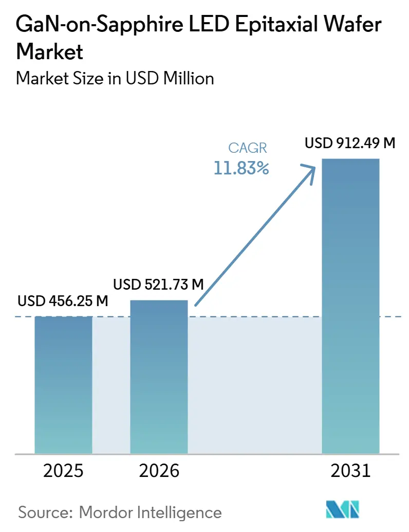
| Market Size (2026) | USD 521.73 Million |
| Market Size (2031) | USD 912.49 Million |
| Growth Rate (2026 - 2031) | 11.83% CAGR |
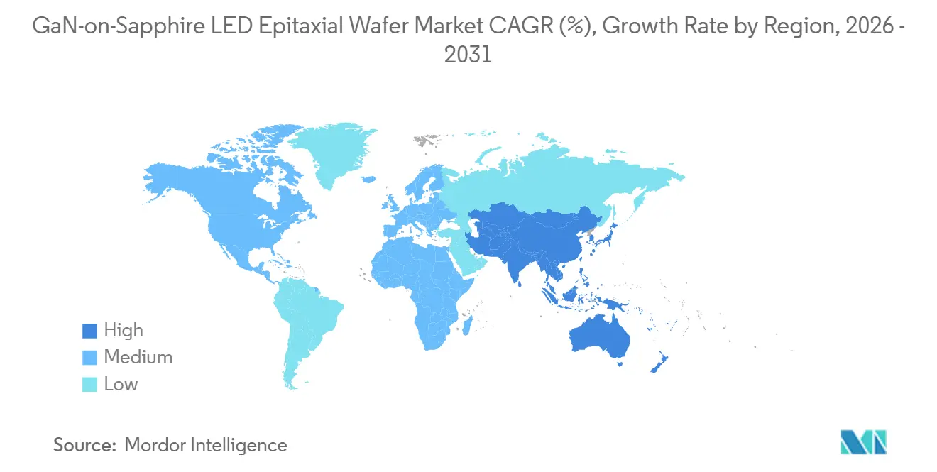
| Fastest Growing Market | Asia Pacific |
| Largest Market | Asia Pacific |
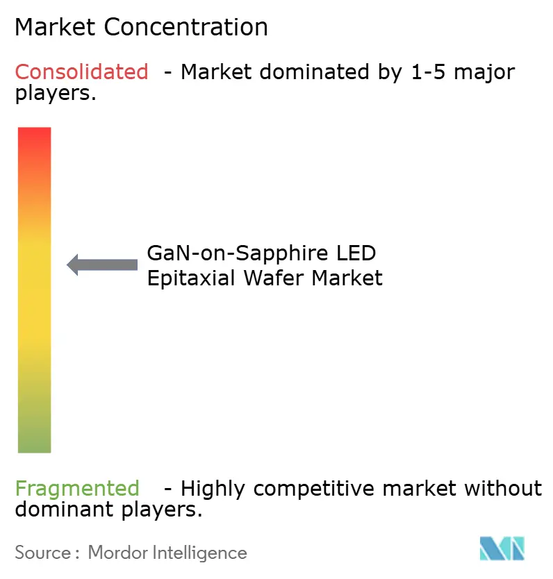
| Market Concentration | Medium |
Major Players *Disclaimer: Major Players sorted in no particular order Image © Mordor Intelligence. Reuse requires attribution under CC BY 4.0. | |
GaN-on-Sapphire LED Epitaxial Wafer Market Analysis by Mordor Intelligence
The GaN-on-Sapphire LED Epitaxial Wafer market size is expected to increase from USD 456.25 million in 2025 to USD 521.73 million in 2026 and reach USD 912.49 million by 2031, growing at a CAGR of 11.83% over 2026-2031. Demand is pivoting toward higher-brightness, narrower-wavelength dies that require tighter epitaxial uniformity than legacy lighting designs. Volume adoption in mini-LED and micro-LED displays, ultraviolet-C sterilization modules, and Li-Fi optical-communication prototypes is accelerating 150 mm production, while government incentives in Asia-Pacific, Europe, and North America continue to subsidize compound-semiconductor fabs. Cost deflation in 150 mm wafers, ongoing device integration for automotive adaptive headlamps, and sapphire’s superior thermal conductivity relative to silicon reinforce the structural growth path of the GaN-on-Sapphire LED Epitaxial Wafer market. Competitive strategies emphasize vertical integration into sapphire substrates and proprietary metal-organic chemical-vapor-deposition (MOCVD) recipes that preserve margin despite pricing pressure from emerging GaN-on-silicon alternatives.
Key Report Takeaways
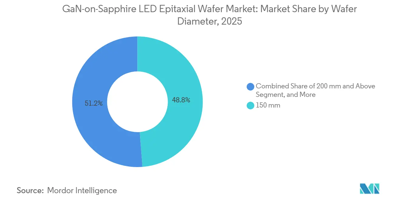
- By wafer diameter, the 150 mm segment commanded 48.78% of the GaN-on-Sapphire LED Epitaxial Wafer market share in 2025, while 200 mm and above wafers are projected to expand at a 12.84% CAGR through 2031.
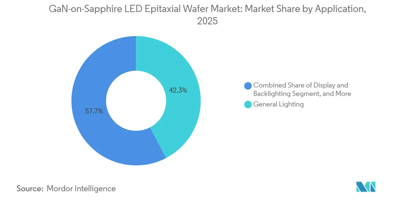
- By application, general lighting led with 42.31% revenue share in 2025; display and backlighting are advancing at a 12.58% CAGR between 2026 and 2031.
- By geography, Asia-Pacific held 66.85% of revenue in 2025, and the region is forecast to expand at a 12.75% CAGR over 2026-2031.
Note: Market size and forecast figures in this report are generated using Mordor Intelligence’s proprietary estimation framework, updated with the latest available data and insights as of January 2026.
Global GaN-on-Sapphire LED Epitaxial Wafer Market Trends and Insights
Drivers Impact Analysis*
| Driver | (~) % Impact on CAGR Forecast | Geographic Relevance | Impact Timeline |
|---|---|---|---|
| Increasing Penetration of Mini and Micro-LED Displays | +3.2% | Asia-Pacific core, spillover to North America | Medium term (2-4 years) |
| Rapid Shift Toward Phosphor-Free Ultra-High-Brightness Lighting | +2.5% | Global, early adoption in Europe and Japan | Medium term (2-4 years) |
| Cost Downward Trend in 150 mm GaN-on-Sapphire Wafers | +2.1% | Asia-Pacific manufacturing hubs | Short term (≤ 2 years) |
| Government Incentives for Compound-Semiconductor Fabs | +1.8% | Europe, North America, Japan, South Korea | Long term (≥ 4 years) |
| Adoption of GaN Epilayers for UV-C Sterilization LEDs | +1.4% | Global healthcare and municipal water | Medium term (2-4 years) |
| Integration of GaN LEDs in Li-Fi Optical Communications | +0.9% | North America and Europe pilots | Long term (≥ 4 years) |
| Source: Mordor Intelligence | |||
Increasing Penetration of Mini and Micro-LED Displays
Premium television brands now mount between 10,000 and 25,000 mini-LED dies per panel, unlocking more than 2,000 local-dimming zones that edge-lit backlights cannot match.[1]Nichia Corporation, “Nichia Develops 2-Chip White LED for LCD Backlighting,” NICHIA.CO.JP Ennostar’s 2025 merger integrated over 400 metal-organic chemical-vapor-deposition (MOCVD) reactors into a single supply chain, ensuring wafer availability for Apple and Samsung and tightening epitaxial process control. PlayNitride and Plessey use monolithic micro-LED arrays on sapphire to bypass the mass-transfer yield losses that plague hybrid silicon-backplane approaches, positioning their technology for augmented-reality headsets. Automotive cockpits are also shifting to micro-LED clusters that achieve daylight-readable luminance above 10,000 candelas per square meter, a specification conventional phosphor-converted white LEDs struggle to meet within thermal limits. Together, these deployments create sustained demand for uniform GaN-on-sapphire epitaxial wafers that support tight wavelength binning and low forward-voltage spread.
Rapid Shift Toward Phosphor-Free Ultra-High-Brightness Lighting
Architectural and horticultural fixtures are migrating to direct-emission red-green-blue clusters that eliminate the 15-25% energy loss from yellow-phosphor down-conversion. Research published in 2024 showed external quantum efficiencies reaching 52.4% for blue and 25.2% for green quantum wells on sapphire, roughly doubling 2010 performance benchmarks. Europe’s Ecodesign Directive, active since January 2025, raises minimum efficacy to 210 lumens per watt by 2027, accelerating interest in phosphor-free arrays that meet the target without complex thermal management.[2]European Commission, “Commission Welcomes Political Agreement on European Chips Act,” EUROPA.EU San’an Optoelectronics earmarked 40% of its CNY 11.6 billion Hubei expansion for narrow-band red and green dies optimized for horticulture, underlining the commercial pull of these higher-brightness devices. The convergence of regulatory pressure, quantum-well efficiency gains, and capacity expansions positions phosphor-free lighting as a durable growth engine for GaN-on-sapphire wafers.
Cost Downward Trend in 150 mm GaN-on-Sapphire Wafers
Average selling prices for 150 mm wafers fell below USD 40 in 2025 after manufacturers introduced substrate-recycling programs and optimized batch-reactor utilization. Ennostar’s NT$5.4 billion automation upgrade cut epitaxial-thickness variation to under 2%, enabling tighter wavelength bins that raise die-level yields and offset pricing pressure. Veeco’s Propel300 platform, configured for 8×150 mm runs, delivers 20% higher throughput than earlier TurboDisc tools, reducing cost per wafer once depreciation is factored in.[3]Veeco Instruments, “Veeco Receives First Propel 300 GaN MOCVD System Order,” VEECO.COM Because threading-dislocation densities on 150 mm sapphire remain below 5 × 10⁸ cm⁻², device makers avoid the yield penalty that still plagues larger diameters. The resulting price-to-performance advantage keeps 150 mm formats entrenched in general-lighting, automotive, and entry-level display contracts.
Government Incentives for Compound-Semiconductor Fabs
Public funding is lowering the effective capital intensity of new GaN fabs by up to 40%. The EUR 43 billion European Chips Act reserves a portion specifically for gallium nitride and silicon carbide production lines, widening regional wafer supply. Japan’s Ministry of Economy, Trade and Industry now covers as much as 50% of construction costs, directly supporting Nichia’s vertical integration into sapphire substrates. South Korea’s KRW 17 trillion K-Semiconductor program targets a 30% global share of wide-bandgap devices by 2030, channeling grants toward 200 mm-capable MOCVD reactors. In the United States, the CHIPS and Science Act funds of USD 52 billion, while dispersed across materials, include provisions for compound semiconductors that have already triggered the first domestic Propel300 order. These incentives are accelerating capacity ramps by incumbent and second-tier suppliers alike, expanding the geographic footprint of GaN-on-sapphire production.
Restraints Impact Analysis*
| Restraint | (~) % Impact on CAGR Forecast | Geographic Relevance | Impact Timeline |
|---|---|---|---|
| Thermal Mismatch-Driven Yield Losses Above 200 mm | –1.9% | Global, particularly Asia-Pacific fabs | Short term (≤ 2 years) |
| Supply Constraints of High-Purity Sapphire Substrates | –1.5% | Global bottlenecks in Russia and China | Medium term (2-4 years) |
| Capital-Intensive MOCVD Tooling for Uniform Thick GaN Layers | –1.2% | Global new entrants | Long term (≥ 4 years) |
| Competition from Emerging GaN-on-Si Platforms in TV Backlighting | –0.8% | Asia-Pacific, spillover to North America | Medium term (2-4 years) |
| Source: Mordor Intelligence | |||
Thermal Mismatch-Driven Yield Losses Above 200 mm
Sapphire’s thermal-expansion coefficient of 7.5 × 10⁻⁶ K⁻¹ versus gallium-nitride’s 5.6 × 10⁻⁶ K⁻¹ induces residual compressive stress between –1.0 and –1.5 GPa in epilayers thicker than 5 µm, increasing bow and crack rates on 200 mm wafers. December 2024 Nanomaterials research documented macro-crack densities above 0.3 cm⁻² when the GaN thickness exceeded 20 µm on 200 mm sapphire wafers, rendering such wafers unsuitable for high-power LEDs. Patterned substrates and compliant AlN buffers mitigate bow below 50 µm but add 15-20% cycle time and raise consumable costs. Display manufacturers, therefore, continue to specify 150 mm wafers for mini-LED backlights despite the 78% area advantage of 200 mm formats. Until stress-management techniques mature, wafer-level economics favor smaller diameters, tempering near-term transition plans.
Supply Constraints of High-Purity Sapphire Substrates
Crystalwise, Monocrystal, and Rubicon collectively supply more than 70% of LED-grade sapphire, yet their combined Kyropoulos furnace capacity still trails demand spikes from mini-LED television launches. Russian alumina feedstock disruptions in 2024 extended lead times from eight to 14 weeks, forcing wafer producers to double substrate inventories. Spot prices ranged from USD 8 to USD 14 per 150 mm wafer in 2025, resulting in 20-35% variability in epitaxial wafer quotations. San’an Optoelectronics aims to internalize 40% of its substrate needs by 2027, but the three-year furnace commissioning cycle limits immediate relief. Price volatility complicates long-term agreements with automotive and display customers, constraining aggressive short- to medium-term capacity expansion.
*Our forecasts treat driver/restraint impacts as directional, not additive. The impact forecasts reflect baseline growth, mix effects, and variable interactions.
Segment Analysis
By Wafer Diameter: Economies Collide with Defect Physics
The 150 mm format captured 48.78% of GaN-on-Sapphire LED Epitaxial Wafer market share in 2025, reflecting its balance between area throughput and threading-dislocation densities that stay within the 3 × 10⁸–5 × 10⁸ cm⁻² range. Automotive adaptive-beam modules value this uniformity because forward-voltage spread remains under ±50 mV, keeping thermal budgets manageable at kilohertz drive frequencies. Ennostar’s fleet of more than 400 MOCVD chambers is still tooled for 150 mm, as retrofitting a single reactor to 200 mm costs USD 2-3 million and disrupts qualified process flows. Veeco’s Propel300 platform delivers 20% throughput in its 8×150 mm configuration, reducing depreciation per wafer and locking in the cost advantage of the larger diameter. As a result, the GaN-on-Sapphire LED Epitaxial Wafer market size for 150 mm wafers is expected to remain the revenue anchor through the middle of the forecast window, even though its proportional share declines.
Adoption of 200 mm and larger wafers is projected to rise at a 12.84% CAGR to 2031 as display makers seek the 78% area gain per slice, yet residual compressive stress often exceeds –1.2 GPa and elevates macro-crack density beyond 0.3 cm⁻² when GaN exceeds 20 µm. Patterned-sapphire substrates and compliant AlN buffers reduce bow below 50 µm but add 15-20% process time, muting the per-die savings. Up to 100 mm formats are available for ultraviolet-C LEDs, with tight control of aluminum composition enabling≥5% wall-plug efficiency at 265 nm for portable sterilizers. Equipment vendors support 5×200 mm batch loads, yet early adopters report that defect-attributed scrap negates much of the theoretical cost benefit, especially for high-power dies. Until yield-engineering breakthroughs emerge, buyers will continue to split orders between 150 mm for mature products and 200 mm for bleeding-edge displays, limiting abrupt share shifts within the GaN-on-Sapphire LED Epitaxial Wafer market.


By Application: Display Backlighting Outpaces Legacy Lighting
General lighting commanded 42.31% of revenue in 2025, leveraging the proven lumen-per-watt economics of blue dies paired with yellow-phosphor converters under efficacy rules such as Europe’s 210 lm/W threshold for commercial fixtures. Yet retrofit saturation in developed economies is slowing volume growth, and municipal procurement cycles are lengthening as luminaires already installed after 2020 near their 50,000-hour lifetime. Blue-green-red phosphor-free clusters on sapphire are gaining share within stadium, horticulture, and industrial lighting because they avoid the 15-25% Stokes-shift loss and unlock more precise spectral tuning. Cost-optimized 150 mm wafers keep the bill of materials acceptable to contractors, while the reduced thermal resistance of sapphire compared to silicon supports dense chip-on-board arrays without active cooling. Consequently, the GaN-on-Sapphire LED Epitaxial Wafer market size linked to lighting will continue to rise, but at a pace well below the headline CAGR.
Display and backlighting is the fastest-moving use case, advancing at a 12.58% CAGR as premium televisions and monitors migrate from edge-lit panels to direct-backlight mini-LED matrices that require 10,000-25,000 dies per screen. Nichia’s NS2W806H-B2 two-chip emitter removes yellow-phosphor droop, delivering 120 lm/W at 350 mA and permitting thinner optical stacks that improve contrast. Tablet and laptop vendors are following television leaders, while automotive instrument clusters are adopting micro-LED arrays that achieve 10,000 cd/m² of daylight readability. Specialty sub-segments such as ultraviolet-C disinfection modules and Li-Fi transceivers add incremental volume, with aluminum gallium nitride (AlGaN) epilayers on sapphire proving essential for ≥1 GHz modulation bandwidths. These converging demands are set to push the display-oriented share of GaN-on-Sapphire LED Epitaxial Wafer market share steadily higher through 2031, tightening the supply balance for lighting and automotive buyers in peak quarters.
Geography Analysis
Asia-Pacific accounted for 66.85% of global revenue in 2025, and the regional GaN-on-Sapphire LED Epitaxial Wafer market is projected to grow at a 12.75% CAGR through 2031. Taiwan anchors exports, with Ennostar operating more than 400 metal-organic chemical-vapor-deposition reactors across multiple sites after its 2025 merger. China complements this scale; San’an Optoelectronics processed about 24 million wafers in 2025 and is investing CNY 11.6 billion to ramp a Hubei mini-LED campus. Japan’s subsidy program covering up to 50% of compound-semiconductor fab costs underpins Nichia’s vertical move into sapphire substrates, helping shield the region from raw-material shocks. Together, these initiatives preserve Asia-Pacific’s lead in the GaN-on-Sapphire LED Epitaxial Wafer market size over the forecast horizon.
North America is regaining footing as the CHIPS and Science Act channels USD 52 billion into domestic fabs. Veeco Instruments shipped its first Propel300 GaN system to a U.S. power-electronics customer in 2024, signaling the launch of fresh epitaxial capacity. San’an’s planned USD 239 million acquisition of Lumileds folds North American automotive-lighting contracts into a Chinese supply chain, boosting the region’s integration depth. These moves could lift the continent’s GaN-on-Sapphire LED Epitaxial Wafer market share by the late 2020s, although reliance on Asian substrate imports remains a near-term constraint.
Europe captured a modest slice of 2025 revenue but benefits from the EUR 43 billion Chips Act, which allocates funds for gallium nitride and silicon carbide lines. Osram’s EVIYOS adaptive-beam platform exemplifies the region’s focus on high-value automotive dies that justify premium wafer pricing. Vertical-farming projects across Germany, the Netherlands, and France are adopting horticultural mini-LED arrays, driving specialty demand. The rest of the World, Latin America, the Middle East, and Africa remain nascent, yet pilot ultraviolet-C water-treatment schemes are creating beachheads where sapphire’s thermal advantage over silicon is critical. Collectively, these pockets contribute incremental volume but are unlikely to displace Asia-Pacific's dominance in the GaN-on-Sapphire LED Epitaxial Wafer market.

Competitive Landscape
Five vertically integrated suppliers, Nichia, Ennostar, San’an Optoelectronics, Seoul Semiconductor, and Osram, controlled around 65% of global wafer capacity in 2025, operating more than 1,200 MOCVD chambers. San’an strengthened its position by agreeing to purchase Lumileds for USD 239 million, adding North American automotive lighting customers while leveraging lower-cost Chinese manufacturing. The deal also widens San’an’s access to high-margin adaptive-headlamp dies.
Nichia safeguards margin through deep vertical integration; its Nisshin Sapphire subsidiary secures substrate supply and supports a roadmap that now features the NS2W806H-B2 two-chip emitter for mini-LED televisions. Ennostar invests NT$5.4 billion in automated mini-LED lines that cut epitaxial-thickness variance to below 2%, lifting sellable yield on 150 mm wafers. Seoul Semiconductor expands its Wicop and SunLike product families, capitalizing on phosphor-free trends that require tight wavelength bins, while Osram focuses on pixel-dense dies for automotive adaptive-beam modules.
Emerging challengers are attacking niche opportunities rather than head-to-head scale. Plessey and PlayNitride deploy monolithic micro-LED arrays on sapphire, bypassing mass-transfer losses and winning contracts for augmented-reality headsets. Aledia and other GaN-on-silicon proponents promise 40% wafer-level cost cuts at 300 mm, but 17% lattice mismatch still pushes dislocation density beyond reliability targets. Equipment innovation remains a competitive lever: Veeco’s Propel300 enables real-time quantum-well correction that narrows wavelength variance to ±2 nm, a feature incumbents guard closely. With most leaders synchronizing substrate, epitaxy, and packaging under one roof, incremental process IP rather than sheer reactor count is becoming the decisive factor in capturing new opportunities in the GaN-on-Sapphire LED Epitaxial Wafer market.
GaN-on-Sapphire LED Epitaxial Wafer Industry Leaders
Nichia Corporation
Osram Opto Semiconductors GmbH
Cree LED, Inc.
Samsung LED Co., Ltd.
Seoul Semiconductor Co., Ltd.
- *Disclaimer: Major Players sorted in no particular order

Recent Industry Developments
- October 2025: Epistar and Lextar completed their merger to form Ennostar, uniting more than 400 MOCVD reactors across six Asian sites to streamline display-panel wafer supply.
- August 2025: San’an Optoelectronics agreed to buy Lumileds for USD 239 million, with closing slated for Q1 2026.
- August 2025: San’an brought an 8-inch silicon-carbide line online in Hunan, complementing 2,000 wafers-per-month of GaN-on-silicon capacity.
- January 2025: Nichia introduced the NS2W806H-B2 two-chip white LED that delivers 120 lm/W at 350 mA for mini-LED TV backlighting.


Global GaN-on-Sapphire LED Epitaxial Wafer Market Report Scope
The GaN-on-Sapphire LED Epitaxial Wafer Market Report is Segmented by Wafer Diameter (Up to 100 mm, 150 mm, 200 mm and Above), Application (General Lighting, Automotive Lighting, Display and Backlighting, Specialty and Industrial Lighting), and Geography (North America, Europe, Asia-Pacific, Rest of the World). Market Forecasts are Provided in Terms of Value (USD).
| Upto 100 mm |
| 150 mm |
| 200 mm and Above |
| General Lighting |
| Automotive Lighting |
| Display and Backlighting |
| Specialty and Industrial Lighting |
| North America |
| Europe |
| Asia-Pacific |
| Rest of the World |
| By Wafer Diameter | Upto 100 mm |
| 150 mm | |
| 200 mm and Above | |
| By Application | General Lighting |
| Automotive Lighting | |
| Display and Backlighting | |
| Specialty and Industrial Lighting | |
| By Geography | North America |
| Europe | |
| Asia-Pacific | |
| Rest of the World |


Key Questions Answered in the Report
How large will global demand for GaN-on-Sapphire LED wafers be by 2031?
The GaN-on-Sapphire LED Epitaxial Wafer market is forecast to reach USD 912.49 million by 2031, reflecting an 11.83% CAGR from 2026.
Which wafer diameter is currently dominant?
150 mm wafers held 48.78% revenue share in 2025 because they balance area efficiency with lower defect density.
What is the fastest growing end-use segment?
Display and backlighting applications are projected to advance at a 12.58% CAGR through 2031 as premium TVs migrate to mini-LED technology.
Which region contributes the most revenue today?
Asia-Pacific generated 66.85% of global revenue in 2025 and is expected to grow at 12.75% CAGR to 2031.
Who are the top suppliers?
Nichia, Ennostar, San’an Optoelectronics, Seoul Semiconductor, and Osram collectively operate more than 1,200 MOCVD reactors and account for roughly 65% of capacity.
What key restraint limits 200 mm wafer adoption?
Thermal-mismatch stress between sapphire and gallium-nitride causes elevated crack and defect rates on 200 mm wafers, raising costs and limiting high-volume yields.
Page last updated on:


