GaN-Based LED Epitaxial Wafers Market Size and Share
Market Overview
| Study Period | 2020 - 2031 |
|---|---|
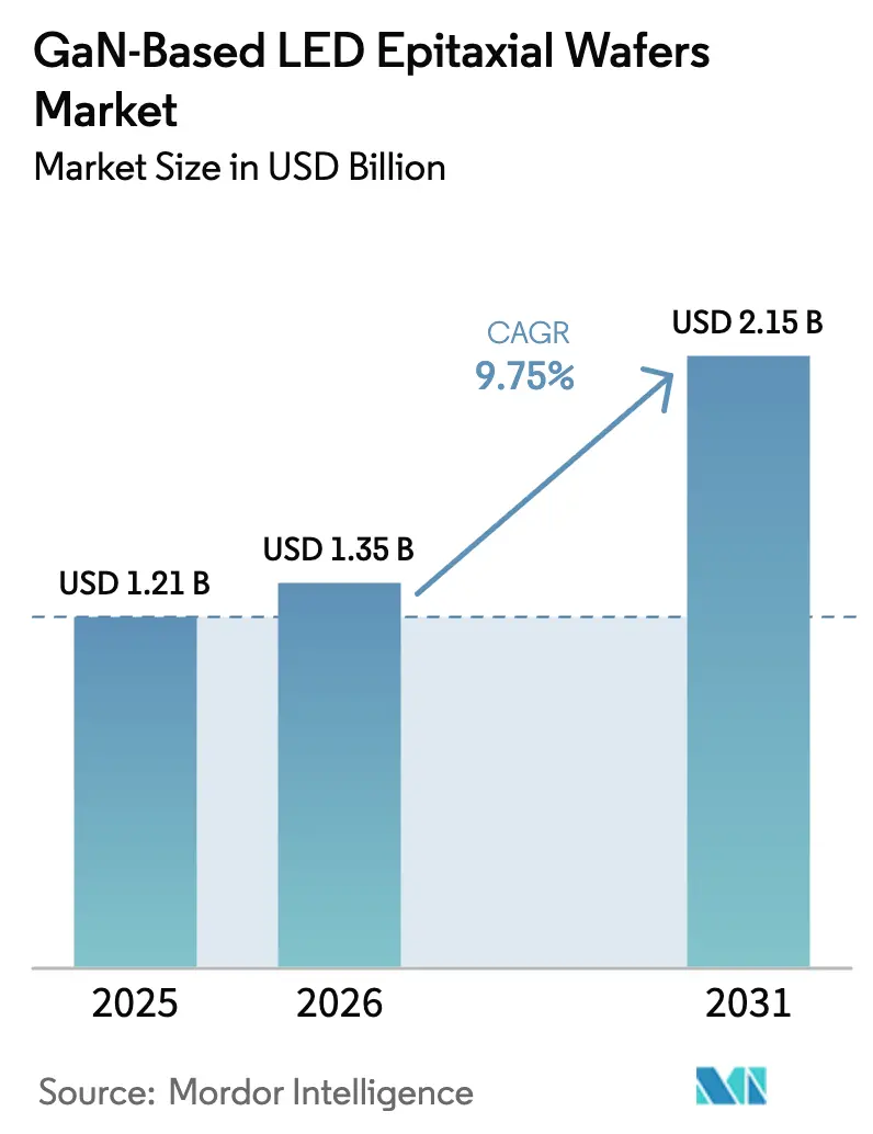
| Market Size (2026) | USD 1.35 Billion |
| Market Size (2031) | USD 2.15 Billion |
| Growth Rate (2026 - 2031) | 9.75% CAGR |
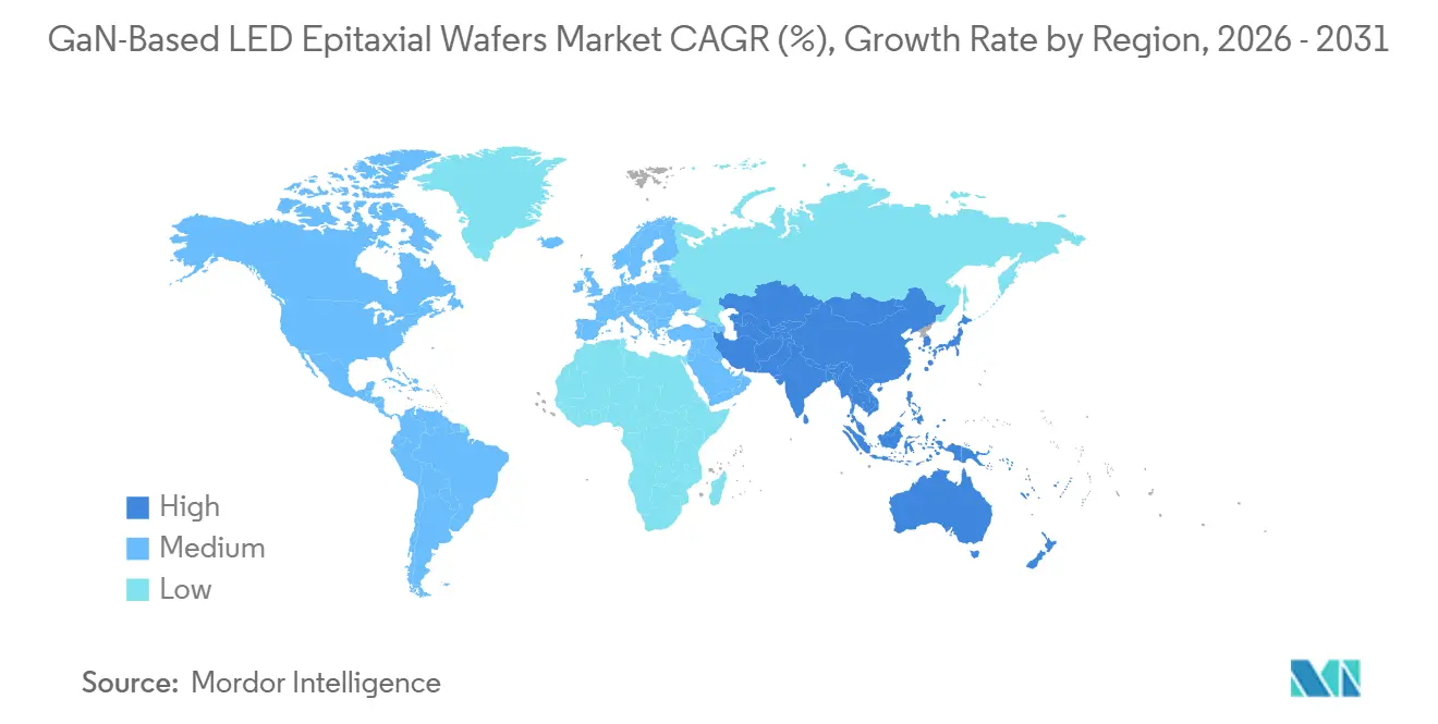
| Fastest Growing Market | Asia Pacific |
| Largest Market | Asia Pacific |
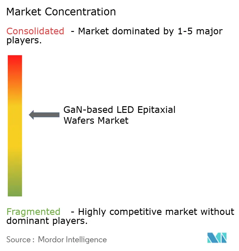
| Market Concentration | Medium |
Major Players *Disclaimer: Major Players sorted in no particular order Image © Mordor Intelligence. Reuse requires attribution under CC BY 4.0. | |
GaN-Based LED Epitaxial Wafers Market Analysis by Mordor Intelligence
The GaN-based LED epitaxial wafers market size is expected to increase from USD 1.35 billion in 2026 to USD 2.15 billion by 2031, growing at a CAGR of 9.75% over 2026-2031. Demand is rising as metal-organic chemical vapor deposition platforms mature, mini-LED and micro-LED display adoption accelerates, and electric-vehicle headlamp content climbs. Suppliers are shifting capacity from commodity general-lighting wafers toward high-value optoelectronic, sensing and automotive substrates that carry tighter wavelength-uniformity and defect specifications. Equipment makers are unlocking cost advantages on 200 mm and 300 mm formats, while vertically integrated Asia-Pacific players leverage upstream crystal-growth control and downstream packaging to compress development cycles.
Key Report Takeaways
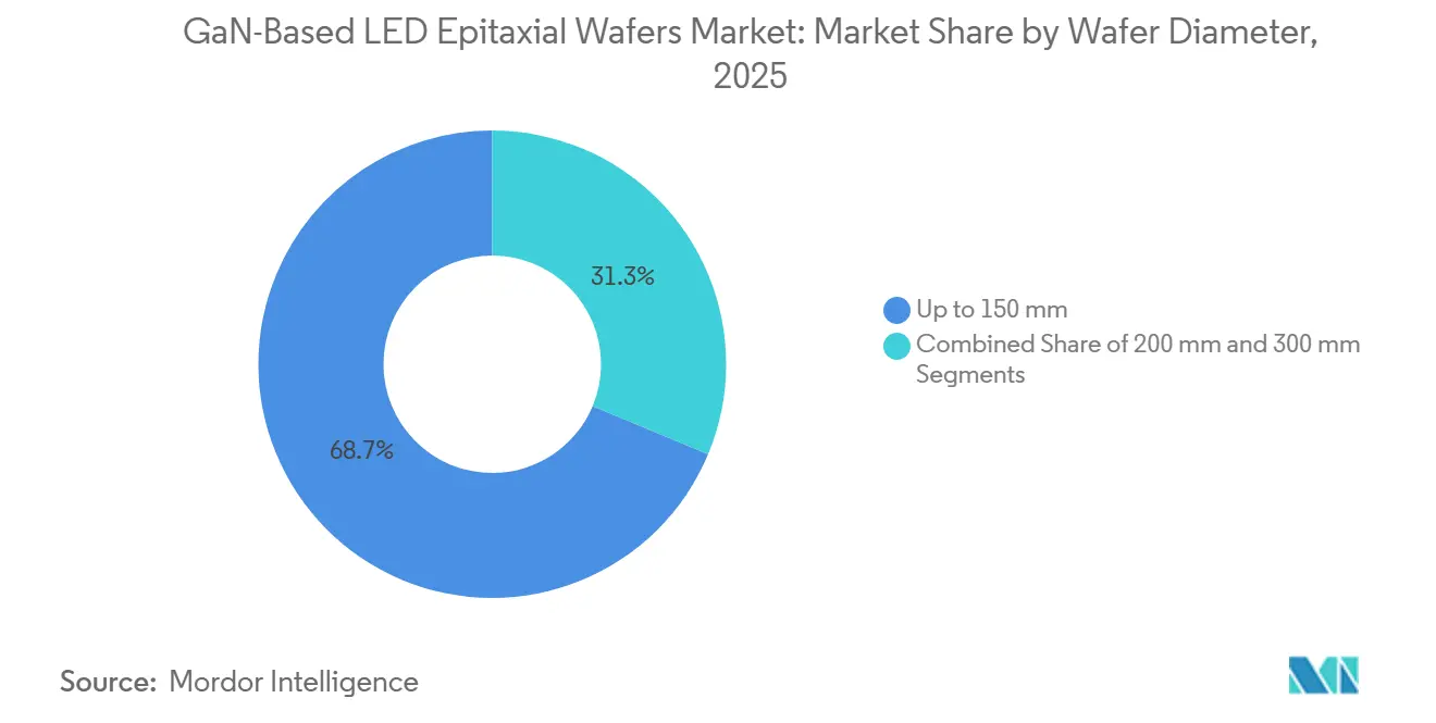
- By wafer diameter, up-to-150 mm formats led with 68.71% revenue share in 2025, whereas 300 mm platforms are projected to expand at a 10.89% CAGR through 2031.
- By semiconductor device type, optoelectronics held 44.28% of the GaN-based LED epitaxial wafers market share in 2025; sensors are forecast to grow at a 10.97% CAGR to 2031.
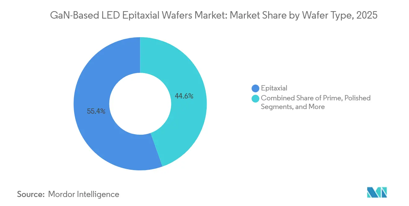
- By wafer type, epitaxial substrates accounted for 55.43% of the GaN-based LED epitaxial wafers market size in 2025, while silicon-on-insulator is set to advance at 10.55% through 2031.
- By end user, consumer electronics captured 41.49% of 2025 revenue; automotive applications are positioned for a 10.68% CAGR between 2026-2031.
- By geography, Asia-Pacific accounted 56.27% of the GaN-based LED epitaxial wafers market size in 2025 and is forecast to grow at a 10.73% CAGR through 2031.
Note: Market size and forecast figures in this report are generated using Mordor Intelligence’s proprietary estimation framework, updated with the latest available data and insights as of January 2026.
Global GaN-Based LED Epitaxial Wafers Market Trends and Insights
Drivers Impact Analysis*
| Driver | (~)% Impact on CAGR Forecast | Geographic Relevance | Impact Timeline |
|---|---|---|---|
| Rapid Penetration of Mini and Micro-LED Displays | +2.8% | Global, with concentration in Asia-Pacific (Taiwan, China, South Korea) and selective North America premium segments | Medium term (2-4 years) |
| Expansion of Electric-Vehicle Headlamp Production | +2.1% | Global, led by Europe and China EV markets, spillover to North America | Medium term (2-4 years) |
| Government Subsidies for Solid-State Lighting Programs | +1.5% | North America, Europe, and select Asia-Pacific markets (Japan, South Korea) | Short term (≤ 2 years) |
| Emerging Use of Free-Standing GaN Substrates to Cut Defects | +1.2% | Global, early adoption in Japan and North America R&D centers, scaling in Asia-Pacific | Long term (≥ 4 years) |
| Shift Toward Au-Free, Cu-Based Metallization to Reduce Cost | +0.9% | Global, with faster adoption in China and Taiwan cost-sensitive manufacturing | Medium term (2-4 years) |
| On-site Regrowth Techniques Enabling Vertical LEDs | +0.7% | Asia-Pacific core (Taiwan, Japan), niche adoption in North America and Europe | Long term (≥ 4 years) |
| Source: Mordor Intelligence | |||
Rapid Penetration of Mini and Micro-LED Displays
Display manufacturers are accelerating mini-LED and micro-LED programs to overcome OLED burn-in limitations and deliver higher peak brightness, driving demand for wafers with sub-5 nm wavelength uniformity on 200 mm and 300 mm diameters. Ennostar announced a 200 mm GaN-on-Si initiative with ALLOS Semiconductors targeting wearable screens exceeding 2,000 PPI.[1]Ennostar, “Ennostar and ALLOS Partner on 200 mm Micro-LED Epitaxy,” ennostar.com Apple has invested USD 334 million with AU Optronics and Epistar in Hsinchu Science Park to secure vertically integrated epitaxial supply for future wearable displays. Automotive cross-pollination is evident in ams OSRAM’s EVIYOS HD25 module, integrated into the NIO ET9, which packs 25,600 micro-LED pixels and requires display-grade epitaxy for 500 m projection.
Expansion of Electric-Vehicle Headlamp Production
Electric-vehicle makers specify adaptive headlamps topping 10,000 pixels, mandating low-defect, high-brightness wafers that survive stringent AEC-Q cycles. The EVIYOS HD25 raises projection distance from 400 m to 500 m and boosts low-beam luminance by 50% for mid-speed driving, illustrating the wafer performance leap required.[2]ams OSRAM, “EVIYOS HD25 Intelligent Headlamp Module,” ams-osram.com Premium EVs now incorporate more than 100 LED packages, each drawing epitaxial material that must maintain chromatic stability across wide temperature swings.
Government Subsidies for Solid-State Lighting Programs
The United States Department of Energy’s Next Generation Lighting Initiative funds GaN epitaxy uniformity research and pilot-line tooling, lowering risk for novel substrates and metrology. Complementary European efficiency mandates are phasing out legacy lighting, driving advanced LED modules into municipal and commercial retrofits. The combination of direct subsidies for manufacturing capacity and indirect demand stimulus through efficiency mandates compresses the adoption timeline for advanced epitaxial processes, enabling suppliers to amortize MOCVD tool investments over larger production volumes.
Emerging Use of Free-Standing GaN Substrates
Sumitomo Electric commercialized 4-inch and 6-inch free-standing GaN wafers using QF-HVPE, achieving dislocation densities below 10^6 cm-2 in vertical LEDs and power devices. AIXTRON’s vertical HVPE reactors demonstrated >100 µm/h growth rates, overcoming historical throughput constraints. Lower defectivity directly raises micro-LED transfer yields and extends high-power device lifetimes, providing long-term cost relief despite higher substrate expense.
Restraints Impact Analysis*
| Restraint | (~)% Impact on CAGR Forecast | Geographic Relevance | Impact Timeline |
|---|---|---|---|
| Capital-Intensive MOCVD Tool Upgrades | -1.8% | Global, acute in emerging manufacturing regions lacking depreciated equipment bases | Short term (≤ 2 years) |
| Supply Volatility of High-Purity Sapphire Boules | -1.3% | Global, with pronounced effects in Asia-Pacific due to concentration of sapphire suppliers | Short term (≤ 2 years) |
| Thermal Management Challenges on 300 mm Platforms | -0.9% | Global, particularly North America and Europe foundries scaling 300 mm GaN-on-Si | Medium term (2-4 years) |
| IP Fragmentation Around Patterned Sapphire Substrates | -0.6% | Global, with litigation concentrated in North America, Europe, and Japan | Medium term (2-4 years) |
| Source: Mordor Intelligence | |||
Capital-Intensive MOCVD Tool Upgrades
State-of-the-art 300 mm GaN reactors cost more than USD 5 million apiece, while full production clusters require eight to ten tools plus in-situ metrology and robotics. Veeco expects its Propel300 revenues to hit USD 80 million in 2026, implying only a handful of fabs can currently absorb such capital.[3]Veeco Instruments, “Q3 2025 Earnings Presentation,” veeco.com Smaller epitaxial-wafer suppliers face a strategic dilemma: legacy 150-millimeter and 200-millimeter MOCVD tools are fully depreciated and can produce wafers at competitive cash costs, but these platforms cannot match the die-per-wafer economics of 300-millimeter formats, risking margin compression as large foundries scale.
Supply Volatility of High-Purity Sapphire Boules
Sapphire substrate costs account for 15% to 25% of total epitaxial-wafer manufacturing expenses in 150-millimeter formats, and price spikes of 20% to 30% during supply shortages can erode gross margins for wafer suppliers without long-term fixed-price contracts with substrate vendors. The concentration of sapphire boule production among a limited number of suppliers in Asia-Pacific and Eastern Europe creates single points of failure; geopolitical tensions, export restrictions, or natural disasters affecting key production sites can extend lead times from the typical 8 to 12 weeks to 16 weeks or longer. Patterned sapphire substrates face tighter capacity because only select vendors operate lithography-grade cleanrooms.
*Our forecasts treat driver/restraint impacts as directional, not additive. The impact forecasts reflect baseline growth, mix effects, and variable interactions.
Segment Analysis
By Wafer Diameter: Shift Toward Larger Formats Reshapes Cost Curve
Wafers up to 150 mm commanded 68.71% of 2025 revenue, reflecting legacy MOCVD fleets built during the general-lighting boom. The GaN-based LED epitaxial wafers market size for 300 mm substrates is projected to expand at a 10.89% CAGR as foundries chase die-count economies and compatibility with silicon CMOS lines. Mid-scale 200 mm formats bridge current display backlight demand while 300 mm ecosystems mature, exemplified by the Ennostar-ALLOS project aimed at micro-LED wearables. The 300 mm transition is most acute in power and RF, where co-integrating GaN and CMOS drivers on one wafer trims module footprint and cost. However, larger diameters exacerbate thermal non-uniformity, forcing advanced susceptor designs and real-time pyrometry.
Cost dynamics ripple upstream: substrate vendors must now supply 300 mm sapphire and silicon wafers meeting tighter flatness and surface-roughness specs. ROHM Semiconductor and TSMC’s February 2026 alliance leverages existing 300 mm clean-room assets to co-develop GaN power devices, highlighting the pull of shared infrastructure. Yet capital intensity and lengthy automotive qualifications mean widespread 300 mm adoption will remain limited to well-capitalized fabs through the forecast period.


By Semiconductor Device Type: Sensors Narrow the Gap With Optoelectronics
Optoelectronics maintained 44.28% revenue leadership in 2025, anchored by mini-LED backlights and general illumination, but sensors are expected to post a 10.97% CAGR as vertical-cavity surface-emitting lasers and LiDAR sources proliferate. The GaN-based LED epitaxial wafers market share for discrete power devices is rising more gradually, constrained by cost-sensitive charger applications prioritizing price over defect density.
The sensors segment's rapid growth reflects the convergence of automotive safety regulations mandating advanced driver-assistance systems and consumer demand for facial recognition and augmented-reality features in smartphones and wearables. The micro segment, encompassing micro-electromechanical systems and micro-scale photonic devices, is emerging as a wildcard; while current volumes are limited, the potential for GaN-based micro-resonators and photonic integrated circuits to enable chip-scale light detection and ranging could create a new demand vector for ultra-low-defect epitaxial wafers. While optoelectronics will likely remain dominant, its lead narrows as sensing demand accelerates.
By Wafer Type: Epitaxial Substrates Dominate, SOI Picks Up Momentum
Epitaxial wafers captured 55.43% of 2025 revenue because they feed directly into LED die fabrication flows. The GaN-based LED epitaxial wafers market for silicon-on-insulator is poised for 10.55% growth, driven by monolithic micro-LED architectures that embed GaN emitters on CMOS backplanes, eliminating the need for external driver ICs. Prime and polished wafers serve as starting substrates for subsequent epitaxial deposition, and their share is largely determined by the choice of substrate material; sapphire prime wafers dominate for traditional LED applications, while silicon prime wafers are gaining share in GaN-on-silicon power and RF markets.
The silicon-on-insulator segment's growth is tied to the development of monolithic micro-LED displays, where GaN epitaxial layers are transferred onto silicon CMOS backplanes that provide pixel-level addressing and drive circuitry. Specialty sensor-grade wafers demand precise band-gap engineering for ultraviolet or near-infrared detection. Suppliers increasingly specialize in narrow substrate-epitaxy pairings instead of broad catalogues, enabling deeper process optimization but reducing capacity flexibility.
By End User: Automotive Emerges as Fastest-Growing Demand Center
Consumer electronics generated 41.49% of 2025 revenue, spanning mini-LED tablets, smartphone flashes, and smart-TV backlights. Automotive is forecast to grow 10.68% annually as adaptive matrix headlights, in-cabin sensing, and exterior signaling multiply per-vehicle LED count. The GaN-based LED epitaxial wafer market, tied to premium EV headlamps, already commands price premiums because meeting AEC-Q reliability over 15 years requires tight wavelength binning and ultra-low defectivity.
Industrial ultraviolet curing, horticulture, and machine-vision niches expand steadily on the back of wavelength-specific LEDs, while telecom applications purchase wafers for 5G RF amplifiers that demand high linearity. Personal computers and servers represent a mature segment where mini-LED backlights are penetrating premium gaming monitors and professional displays, but growth is constrained by the slower refresh cycles typical of these product categories. The automotive surge represents both volume and margin upside for qualified suppliers.
Geography Analysis
Asia-Pacific held 56.27% of 2025 revenue and is projected to climb at a 10.73% CAGR, underpinned by Taiwan’s vertically integrated clusters and China’s subsidized capacity expansions. Taiwanese firms such as Epistar, Lextar and Ennostar work in close proximity to panel assemblers, accelerating feedback loops vital for micro-LED production. Chinese champion Sanan Optoelectronics is scaling aggressively, aided by state incentives and its pending Lumileds acquisition that unlocks Western automotive channels.
North America and Europe contribute a smaller yet strategic portion of demand. United States DOE funding offsets early-stage risk for novel epitaxial routes, while European automakers require AEC-Q qualified wafers for adaptive headlights, giving local suppliers premium pricing headroom. Technology flows bidirectionally, as European LED innovations like ams OSRAM’s EVIYOS find application in Chinese EVs, underlining the global integration of supply chains.
The Rest of World region, including South America, the Middle East and Africa, remains nascent, relying on imported LED modules for illumination and signage. Nevertheless, government programs aimed at indigenous semiconductor capacity could lift regional wafer demand over the long term, especially if initiatives prioritize compound-semiconductor devices for renewable-energy or telecom-infrastructure goals.

Competitive Landscape
The GaN-based LED epitaxial wafer market is moderately concentrated, with the top five suppliers accounting for more than half of global capacity. Nichia Corporation protects premium pricing through robust patent portfolios and executed a cross-license with ams OSRAM in October 2025 to reduce litigation risk while broadening product breadth. Seoul Semiconductor differentiates through Wicop package-free and SunLike natural-spectrum LEDs, serving niche segments that value spectral uniformity. Sanan Optoelectronics’ USD 239 million purchase of Lumileds signals a push into Western automotive channels, leveraging Lumileds’ AEC-Q credentials and patent estate.
Equipment vendors such as AIXTRON and Veeco Instruments are capturing value by enabling these transitions; AIXTRON's vertical HVPE reactor for free-standing GaN and Veeco's Propel300 platform for 300-millimeter GaN-on-silicon are examples of how tool suppliers are shaping the competitive landscape by determining which epitaxial architectures achieve commercial viability.
Emerging Taiwanese and Chinese foundries are adopting cost-optimized reactors to serve second-tier customers and compete primarily on price. Advanced in-situ reflectometry and automated defect inspection are fast becoming must-have capabilities, as downstream micro-LED transfer yields hinge on sub-ppm defectivity.
GaN-Based LED Epitaxial Wafers Industry Leaders
Nichia Corporation
Osram Opto Semiconductors GmbH
Sanan Optoelectronics Co., Ltd.
Cree Inc.
Ennostar Corporation
- *Disclaimer: Major Players sorted in no particular order

Recent Industry Developments
- February 2026: ROHM Semiconductor and TSMC launch joint 300 mm GaN power-device program leveraging TSMC’s existing fab shell.
- January 2026: Ennostar partners with ALLOS Semiconductors to scale 200 mm GaN-on-Si epitaxy for micro-LED wearables.
- November 2025: Veeco projects 33% YoY growth in 2026 Propel300 revenues to USD 80 million as pilot lines move to production.
- October 2025: Nichia and ams OSRAM sign broad GaN patent cross-license covering epitaxy and phosphor technologies.


Global GaN-Based LED Epitaxial Wafers Market Report Scope
The GaN-based LED Epitaxial Wafers Market refers to the industry focused on the production and supply of gallium nitride (GaN) epitaxial wafers, which are used as substrates for manufacturing LEDs. These wafers are categorized based on diameter, semiconductor device type, wafer type, and end-user applications.
The GaN-based LED Epitaxial Wafers Market Report is Segmented by Wafer Diameter (Up to 150 mm, 200 mm, and 300 mm), Semiconductor Device Type (Logic, Memory, Analog, Discrete, Optoelectronics, Sensors, and Micro), Wafer Type (Prime, Polished, Epitaxial, Silicon-on-Insulator, Specialty Silicon, Power, and Sensor-Grade), End-user (Consumer Electronics, Mobile and Smartphones, PCs and Servers, Industrial, Telecommunications, Automotive, and Other End-user Applications), and Geography (North America, Europe, Asia-Pacific, and Rest of the World). The Market Forecasts are Provided in Terms of Value (USD).
| Up to 150 mm |
| 200 mm |
| 300 mm |
| Logic |
| Memory |
| Analog |
| Discrete |
| Optoelectronics |
| Sensors |
| Micro |
| Prime |
| Polished |
| Epitaxial |
| Silicon-on-Insulator (SOI) |
| Specialty Silicon (High-Resistivity) |
| Power |
| Sensor-Grade |
| Consumer Electronics |
| Mobile and Smartphones |
| PCs and Servers |
| Industrial |
| Telecommunications |
| Automotive |
| Other End-user Applications |
| North America |
| Europe |
| Asia-Pacific |
| Rest of the World |
| By Wafer Diameter | Up to 150 mm |
| 200 mm | |
| 300 mm | |
| By Semiconductor Device Type | Logic |
| Memory | |
| Analog | |
| Discrete | |
| Optoelectronics | |
| Sensors | |
| Micro | |
| By Wafer Type | Prime |
| Polished | |
| Epitaxial | |
| Silicon-on-Insulator (SOI) | |
| Specialty Silicon (High-Resistivity) | |
| Power | |
| Sensor-Grade | |
| By End-user | Consumer Electronics |
| Mobile and Smartphones | |
| PCs and Servers | |
| Industrial | |
| Telecommunications | |
| Automotive | |
| Other End-user Applications | |
| By Geography | North America |
| Europe | |
| Asia-Pacific | |
| Rest of the World |


Key Questions Answered in the Report
How large is the GaN-based LED epitaxial wafers market in 2026?
The market is estimated at USD 1.35 billion in 2026 and is projected to reach USD 2.15 billion by 2031.
What is the forecast CAGR for GaN-based LED epitaxial wafers from 2026-2031?
The CAGR for GaN-based LED epitaxial wafers is projected at 9.75% for the period.
Which wafer diameter is growing the fastest?
300 mm substrates are expected to expand at a 10.89% CAGR as foundries seek die-count efficiencies.
Which end-user segment shows the highest growth potential?
Automotive applications are forecast to grow at 10.68% a year due to adaptive matrix headlights and in-cabin sensing.
What region dominates production capacity?
Asia-Pacific holds 56.27% share thanks to integrated supply chains in Taiwan and China.
Page last updated on:


