Gallium Nitride (GaN) On Silicon Wafer Market Size and Share
Market Overview
| Study Period | 2020 - 2031 |
|---|---|
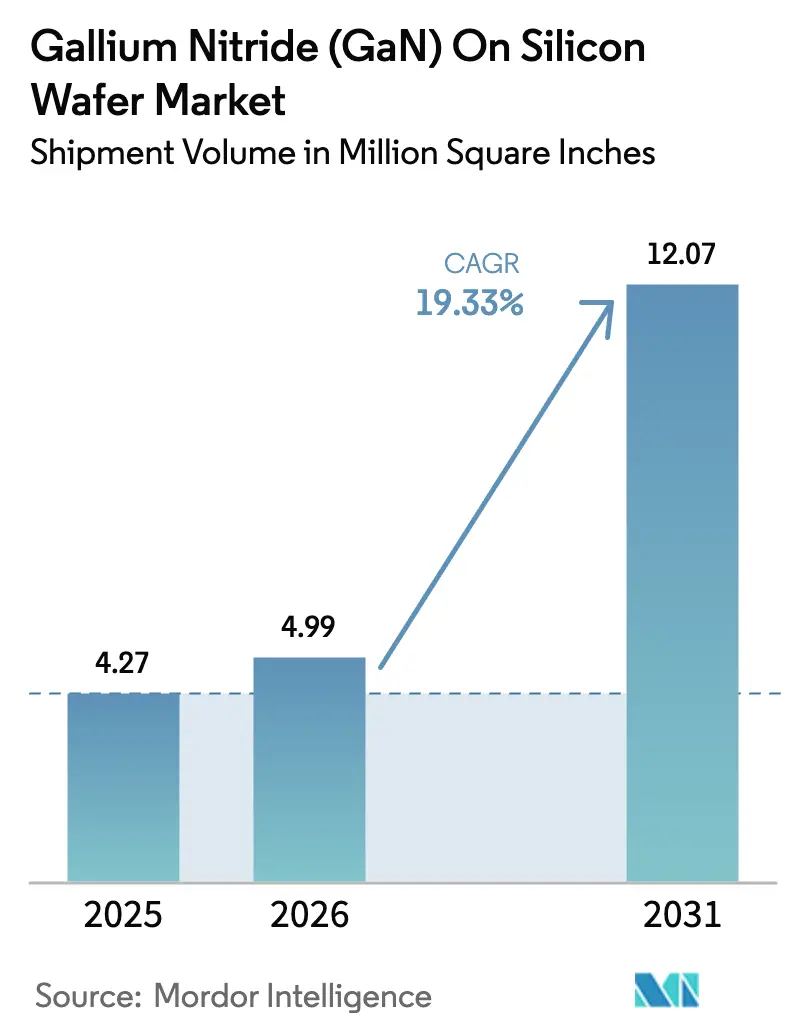
| Market Volume (2026) | 4.99 Million Square Inches |
| Market Volume (2031) | 12.07 Million Square Inches |
| Growth Rate (2026 - 2031) | 19.33% CAGR |
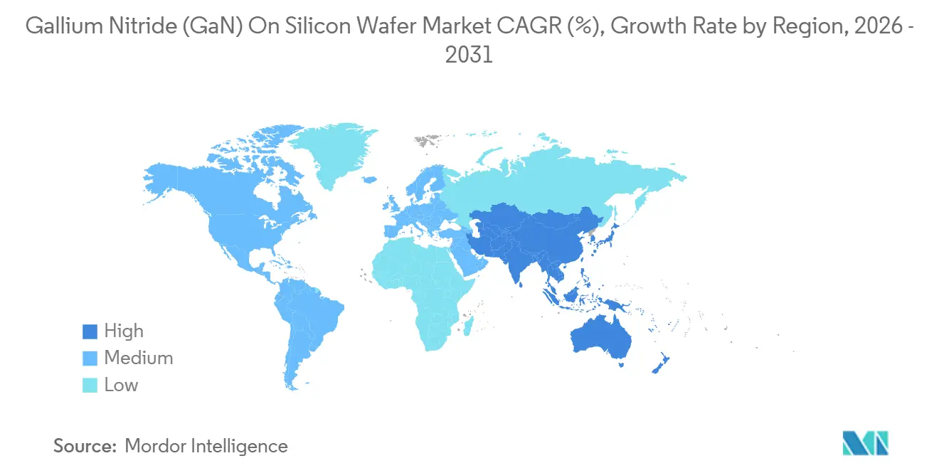
| Fastest Growing Market | Asia Pacific |
| Largest Market | Asia Pacific |
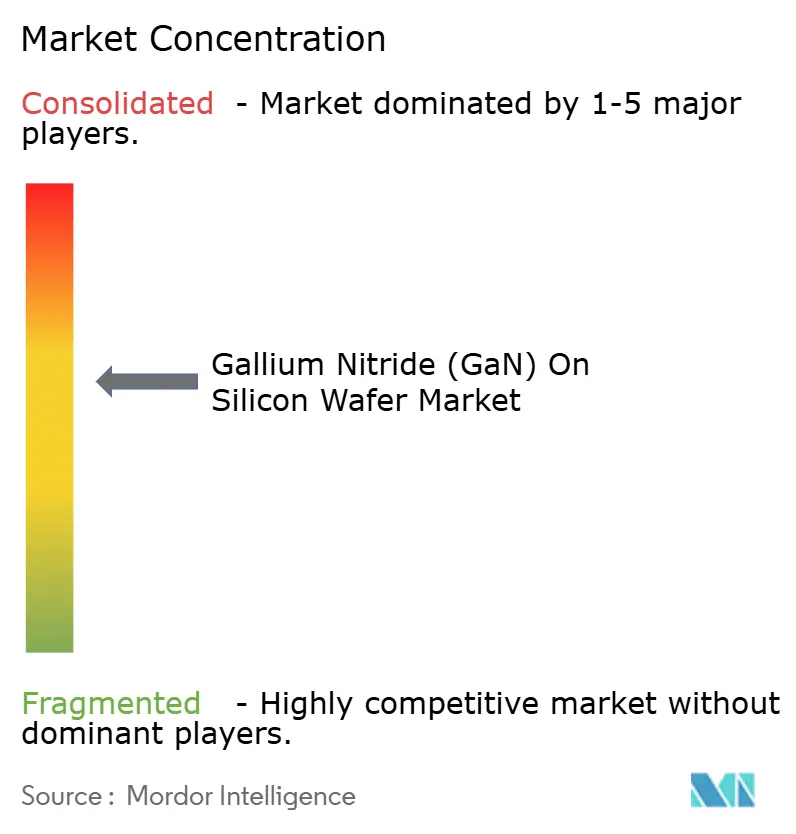
| Market Concentration | Medium |
Major Players *Disclaimer: Major Players sorted in no particular order Image © Mordor Intelligence. Reuse requires attribution under CC BY 4.0. | |
Gallium Nitride (GaN) On Silicon Wafer Market Analysis by Mordor Intelligence
The Gallium Nitride (GaN) on Silicon Wafer market size is expected to increase from 4.27 million square inches in 2025 to 4.99 million square inches in 2026 and reach 12.07 million square inches by 2031, growing at a CAGR of 19.33% over 2026-2031. Robust migration from legacy silicon toward wide-bandgap designs is enabling higher switching frequencies, elevated thermal conductivity, and power densities above 3 kW per cubic inch. Original equipment manufacturers are fast-tracking 200 mm GaN-on-Si qualification in response to 800-volt electric-vehicle traction inverters, mandated USB-C Power Delivery 3.1 fast-charging rules, and satellite-based 5G non-terrestrial network rollouts. Competitive pressure is intensifying as integrated device manufacturers, foundries, and fabless start-ups secure design wins in fast-charging adapters, data-center power supplies, and lidar drivers, while government subsidies in North America and Europe accelerate 300 mm pilot lines and compress commercialization timelines.
Key Report Takeaways
- By end-use industry, consumer electronics commanded 39.46% share in 2025, whereas automotive and electric-vehicle applications are projected to expand at a 20.19% CAGR through 2031.
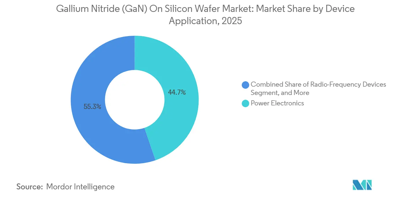
- By device application, power electronics held 44.73% of 2025 shipments while radio-frequency devices are advancing at a 19.93% CAGR to 2031.
- By substrate type, GaN-on-silicon captured 57.49% volume in 2025 and is anticipated to grow at 19.78% through 2031.
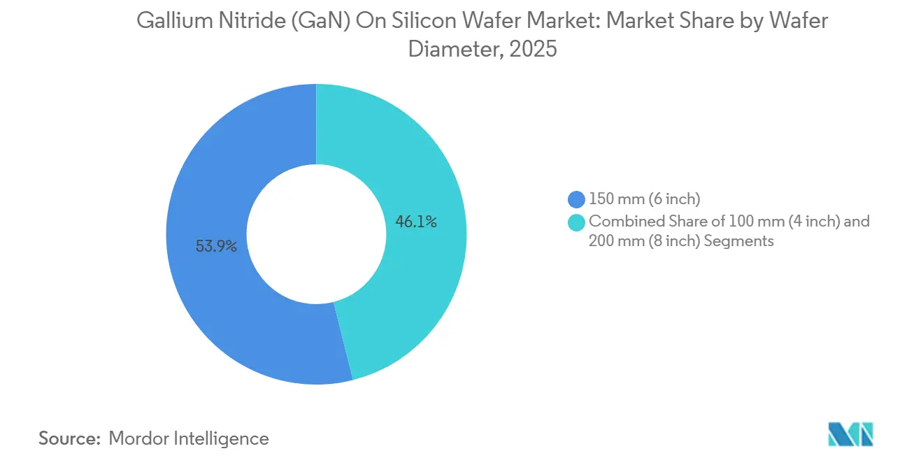
- By wafer diameter, the 150 mm format retained 53.92% share in 2025, yet the 200 mm segment is poised to climb at a 20.37% CAGR to 2031.
- By geography, Asia-Pacific led with 62.53% volume in 2025, and the region is forecast to post a 20.27% CAGR to 2031.
Note: Market size and forecast figures in this report are generated using Mordor Intelligence’s proprietary estimation framework, updated with the latest available data and insights as of January 2026.
Global Gallium Nitride (GaN) On Silicon Wafer Market Trends and Insights
Drivers Impact Analysis*
| Driver | (~) % Impact on CAGR Forecast | Geographic Relevance | Impact Timeline |
|---|---|---|---|
| Maturing 200 mm GaN-on-Si fabrication lines | +4.8% | Global with early leadership in Taiwan, China, Germany | Medium term (2-4 years) |
| Falling epi-wafer costs due to higher MOCVD throughput | +3.6% | Asia-Pacific core, spillover to North America and Europe | Short term (≤ 2 years) |
| Surge in 800 V EV powertrain architectures | +4.2% | Global, concentrated in China, Europe, United States | Medium term (2-4 years) |
| Mandatory USB-C PD 3.1 240 W fast-charging adoption | +3.1% | Global, strongest in Asia-Pacific consumer-electronics hubs | Short term (≤ 2 years) |
| Rising deployment of satellite-based 5G NTN backhaul | +2.4% | Global, with early rollouts in North America, Europe, Middle East | Long term (≥ 4 years) |
| Government incentives for wide-bandgap fabs | +2.9% | North America and Europe, indirect benefits to Asia-Pacific supply chains | Long term (≥ 4 years) |
| Source: Mordor Intelligence | |||
Maturing 200 mm GaN-on-Si Fabrication Lines
Multiple device makers qualified 200 mm GaN-on-Si wafers during 2025, cutting die costs and enabling higher unit volumes. Infineon began customer sampling of 300 mm GaN power devices in late 2025 and targets production by end-2026. Innoscience plans to scale to 20,000 wafers per month on 8-inch lines by 2025 and reach 70,000 by 2030. Navitas and PSMC completed 200 mm qualification in fourth-quarter 2025 and will ramp production in first-half 2026. These moves shorten lead times, support dual-sourcing, and spur adoption in automotive, industrial, and consumer segments. The Gallium Nitride (GaN) on Silicon Wafer market benefits from cost parity with super-junction silicon as scale economies improve.
Falling Epi-Wafer Costs Due to Higher MOCVD Throughput
Tool vendors have released multi-wafer planetary reactors that raise throughput by up to 60%, lowering epitaxial costs by roughly one-third within two years. Veeco’s Propel platform processes eight 200 mm wafers per run with in-situ metrology for tighter process control.[1]Veeco Instruments, “Propel MOCVD Platform for GaN-on-Silicon Epitaxy,” VEECO.COM AIXTRON’s G5+C handles 19 wafers per cycle, reducing cycle time and boosting yield. Lower costs open consumer applications such as USB-C adapters and wireless chargers that were previously bill-of-materials sensitive. Fabless firms can now bid for high-volume designs, expanding the Gallium Nitride (GaN) on Silicon Wafer market footprint across entry-level price points.
Surge in 800 V Electric-Vehicle Powertrain Architectures
Carmakers are upgrading from 400 V to 800 V battery systems to enable 350 kW fast charging and lighter cable harnesses. Qorvo’s 650 V ACT085M065D GaN FET targets onboard chargers and DC-DC converters, shipping since March 2025.[2]Qorvo, “Qorvo Introduces ACT085M065D GaN FET for 800 V Automotive Applications,” QORVO.COM Power Integrations released a 1,250 V GaN switch for high-density data-center rails that share voltage levels with next-gen electric vehicles. Designers choose GaN for its lower gate charge and faster switching speed compared to silicon carbide, enabling smaller passives and higher efficiency. As a result, the Gallium Nitride (GaN) on Silicon Wafer market penetrates traction inverters, onboard chargers, and auxiliary converters at an accelerating pace.
Mandatory USB-C PD 3.1 240 W Fast-Charging Adoption
Global regulators and industry consortia now require USB-C Power Delivery 3.1 as a universal charger interface. Renesas demonstrated a 240 W GaN reference design with 96% efficiency in 2025. D-Link launched a commercial 240 W GaN charger in September 2025, meeting EU common-charger and Indian rules. These mandates guarantee a multi-hundred-million unit opportunity. Adapter suppliers are qualifying multiple GaN-on-Si vendors, adding depth to the Gallium Nitride (GaN) on Silicon Wafer market and quickening price erosion that supports further adoption.
Restraints Impact Analysis*
| Restraint | (~) % Impact on CAGR Forecast | Geographic Relevance | Impact Timeline |
|---|---|---|---|
| Threading dislocations impacting yield beyond 8 inch | -2.7% | Global, most acute in early 200 mm and 300 mm pilot lines | Medium term (2-4 years) |
| Limited availability of 8 inch GaN growth tools | -1.9% | Global, supply concentrated among key MOCVD vendors | Short term (≤ 2 years) |
| IP cross-licensing barriers among IDMs and foundries | -1.4% | Global, especially for new entrants and fabless firms | Long term (≥ 4 years) |
| Thermal mismatch induced wafer bow at ≥200 mm | -1.6% | Global engineering challenge for large-area adopters | Medium term (2-4 years) |
| Source: Mordor Intelligence | |||
Threading Dislocations Impacting Yield Beyond 8 inch
Heteroepitaxial growth on silicon introduces threading dislocations, which degrade the breakdown voltage and increase leakage. Dislocation densities of 1×10⁸ cm⁻² to 5×10⁸ cm⁻² persist at 200 mm, trimming yields by up to 20% in early lots. Longer thermal gradients at 300 mm worsen edge stress and bow, extending qualification and capex. Device makers are adding graded AlGaN buffers and in-situ nitride interlayers, yet the learning curve slows the Gallium Nitride (GaN) on Silicon Wafer market ramp.[3]imec, “imec Launches 300 mm GaN-on-Silicon Pilot Line,” IMEC.INT
Limited Availability of 8 inch GaN Growth Tools
Veeco and AIXTRON supply most 200 mm-class MOCVD reactors, and lead times stretch to 18 months because of complex gas-handling subsystems. The scarcity of ultra-high-purity ammonia and trimethylgallium adds to the constraints. Without sufficient reactors, many IDMs remain on 150 mm, delaying the cost benefits of larger diameters and tempering near-term capacity additions within the Gallium Nitride (GaN) on Silicon Wafer market.
*Our forecasts treat driver/restraint impacts as directional, not additive. The impact forecasts reflect baseline growth, mix effects, and variable interactions.
Segment Analysis
By Wafer Diameter: Economies of Scale Drive 200 mm Transition
The 150 mm format accounted for 53.92% of shipments in 2025 as mature epitaxial recipes and depreciated tool bases supported attractive economics. However, the 200 mm tier is projected to register a 20.37% CAGR through 2031, providing 35-45% die cost savings once yield curves mature. onsemi secured dual-source 200 mm capacity through partnerships with Innoscience and GlobalFoundries, with samples due in first-half of 2026. The Gallium Nitride (GaN) on Silicon Wafer market therefore pivots toward 200 mm as mainstream, while 100 mm remains limited to research and low-volume defense needs.
Infineon’s customer sampling of 300 mm GaN in October 2025 underscores an aggressive scaling roadmap aimed at automotive and industrial volumes. imec’s 300 mm pilot line integrates GaN with advanced CMOS to target single-chip power-management ICs. Early success will depend on mitigating wafer bow and threading dislocations. If process control succeeds, Gallium Nitride (GaN) on Silicon Wafer market size advantages at 300 mm could replicate historical silicon cost curves and accelerate commoditization.


By Substrate Type: Silicon Cost Advantage Sustains Dominance
GaN-on-silicon held 57.49% of 2025 volume and is forecast to grow at 19.78% through 2031, anchored by compatibility with 200 mm and 300 mm silicon fabs and shared precursor supply chains. This cost leadership underpins high-volume consumer and automotive applications, reinforcing dominance within the Gallium Nitride (GaN) on Silicon Wafer market. GaN-on-silicon carbide, despite superior thermal conductivity, remains niche for military radar and satellite transponders where performance trumps a four-fold price premium.
GaN-on-sapphire continues to serve the optoelectronics industry, especially micro-LEDs and ultraviolet emitters. Native GaN substrates deliver the lowest dislocation densities but are cost-prohibitive beyond small research lots. Consequently, market participants allocate R&D to superlattice buffer innovations that raise GaN-on-silicon reliability and extend its addressable voltage up to 1,200 V, keeping the Gallium Nitride (GaN) on Silicon Wafer market share firmly in silicon’s corner.
By Device Application: Power Electronics Lead, RF Gains Traction
Power electronics represented 44.73% of 2025 shipments and are set to expand at 19.93% through 2031 as designers pursue 1 MHz switching and 30 W per cubic-inch power densities. GaN enables smaller inductors and capacitors, improving system cost and thermal headroom in electric-vehicle chargers, solar inverters, and data-center supplies. Radio-frequency devices ride defense modernization and 5G investments, with GlobalFoundries promoting monolithic integration of power and low-noise amplifiers on silicon to cut module bill-of-materials.
Optoelectronics leverages GaN’s direct bandgap for micro-LEDs and lidar diodes, while ultraviolet LEDs address water disinfection. Volume growth in RF and optoelectronics strengthens the product mix, but power electronics remain the primary demand driver for Gallium Nitride (GaN) on Silicon Wafer market size expansion through mid-term forecasts.
By End-Use Industry: Automotive Overtakes Consumer Electronics Growth
Consumer electronics retained the top share at 39.46% in 2025, led by smartphone fast chargers and laptop adapters. Nevertheless, automotive and electric-vehicle demand is growing at 20.19% annually to 2031 as 800 V battery systems permeate mainstream vehicle platforms. Qorvo’s ACT085M065D delivers 11 kW bidirectional charging capability, aligning with vehicle-to-grid roadmaps. Aerospace and defense remain premium niches for high-power RF, while renewable energy systems integrate GaN to hit 98%+ inverter efficiency.
Telecom infrastructure deploys GaN power amplifiers for 5G massive MIMO, and industrial segments target compact uninterruptible power supplies and motor drives. These diversified verticals cushion cyclicality. As automotive overtakes consumer electronics in growth rate, the Gallium Nitride (GaN) on Silicon Wafer market gains resilience and deeper revenue streams.
Geography Analysis
Asia-Pacific accounted for 62.53% of 2025 volume and is slated to grow at a 20.27% CAGR through 2031. China backs Innoscience’s plan to reach 70,000 wafers per month over five years, while Taiwan explores GaN-CMOS integration for mobile and automotive products. Japan leverages decades of compound semiconductor expertise at ROHM, Toshiba, and Mitsubishi Electric, whereas South Korea targets data center and 5G power modules. India offers incentives for pilot lines, but commercial output remains embryonic, so the Gallium Nitride (GaN) on Silicon Wafer market continues to center on East-Asian ecosystems.
North America benefits from USD 52 billion in CHIPS and Science Act funding. MACOM secured preliminary support for a GaN-on-SiC RF line, highlighting the federal commitment to the security of wide-bandgap supply. U.S. foundries collaborate with fabless start-ups to build automotive-grade GaN devices, while Canada advances Arctic surveillance radar programs. Mexican assembly sites co-locate with electric-vehicle plants, extending regionalization advantages within the Gallium Nitride (GaN) on Silicon Wafer market.
Europe advances through EUR 43 billion in EU CHIPS Act resources and EUR 8.1 billion in IPCEI microelectronics grants, funneling capital to Infineon’s 300 mm pilot line and Fraunhofer wide-bandgap projects. France heads an IPCEI cluster on ultra-wide-bandgap materials, and the United Kingdom focuses on RF devices for satellite links. ASML in the Netherlands explores lithography tooling for GaN patterning, while Italy promotes STMicroelectronics’ MasterGaN platform. Outside the core triad, South America, the Middle East, and Africa remain nascent, with isolated renewable-energy pilots using GaN in Brazil and the United Arab Emirates.

Competitive Landscape
The Gallium Nitride (GaN) on Silicon Wafer market is moderately fragmented, with IDMs, foundries, and fabless firms vying for market share. Vertical integration prevails as ONSEMI locks in 200 mm epi-wafer supply through partnerships with Innoscience and GlobalFoundries. Infineon pushes first-mover advantage at 300 mm to win automotive sockets where qualification cycles are longest. Fabless innovators such as Navitas and GaN Systems exploit asset-light models but face allocation risk when capacity tightens.
Differentiation gravitates toward monolithic integration, gate-drive simplicity, avalanche ruggedness, and short-circuit withstand time. Disruptors test superlattice buffers and graded AlGaN transitions to suppress threading dislocations, while incumbents protect intellectual property through cross-licensing.
Patent disputes escalate as new entrants file inter partes review challenges, yet collaboration remains vital to accelerate yield learning at larger diameters. Government subsidies in the United States and Europe raise the entry barrier for latecomers, concentrating influence among firms with deep process integration and capital access, thereby shaping the long-term dynamics of the Gallium Nitride (GaN) on Silicon Wafer market.
Gallium Nitride (GaN) On Silicon Wafer Industry Leaders
Wolfspeed Inc.
Qorvo Inc.
Infineon Technologies AG
STMicroelectronics N.V.
Navitas Semiconductor Corp.
- *Disclaimer: Major Players sorted in no particular order

Recent Industry Developments
- October 2025: Infineon announced customer sampling of 300 mm GaN-on-Si power devices with volume production slated for late 2026.
- October 2025: imec opened a 300 mm GaN-on-Si pilot line aimed at monolithic power-management ICs.
- September 2025: Fraunhofer IAF unveiled 70 nm GaN HEMTs on SiC for satellite communications and defense radar.
- September 2025: D-Link released a 240 W USB-C PD 3.1 GaN charger achieving 96% efficiency.


Global Gallium Nitride (GaN) On Silicon Wafer Market Report Scope
The Gallium Nitride (GaN) on Silicon Wafer Market refers to the industry focused on the production and application of GaN-on-silicon wafers, which serve as substrates for the manufacture of high-performance electronic devices. These wafers are integral to various applications, including power electronics, radio-frequency devices, and optoelectronics, across industries such as automotive, aerospace and defense, renewable energy, consumer electronics, telecommunications, and industrial power systems.
The Gallium Nitride (GaN) on Silicon Wafer Market Report is Segmented by Wafer Diameter (100 mm, 150 mm, and 200 mm), Substrate Type (GaN-on-Silicon, GaN-on-Silicon Carbide, GaN-on-Sapphire, and Native GaN), Device Application (Power Electronics, Radio-Frequency Devices, Optoelectronics, and Other Applications), End-Use Industry (Automotive and EV, Aerospace and Defense, Renewable Energy and Storage, Consumer Electronics, Telecommunications, and Industrial Power Systems), and Geography (North America, Europe, Asia-Pacific, South America, Middle East, and Africa). The Market Forecasts are Provided in Terms of Volume (Square Inches).
| 100 mm (4 inch) |
| 150 mm (6 inch) |
| 200 mm (8 inch) |
| GaN-on-Silicon |
| GaN-on-Silicon Carbide |
| GaN-on-Sapphire |
| Native GaN (Bulk) |
| Power Electronics |
| Radio-Frequency Devices |
| Optoelectronics (LED and Laser) |
| Other Applications |
| Automotive and EV |
| Aerospace and Defense |
| Renewable Energy and Storage |
| Consumer Electronics |
| Telecommunications |
| Industrial Power Systems |
| North America | United States |
| Canada | |
| Mexico | |
| Europe | Germany |
| United Kingdom | |
| France | |
| Rest of Europe | |
| Asia-Pacific | China |
| Japan | |
| India | |
| South Korea | |
| Taiwan | |
| Rest of Asia-Pacific | |
| South America | |
| Middle East | |
| Africa |
| By Wafer Diameter | 100 mm (4 inch) | |
| 150 mm (6 inch) | ||
| 200 mm (8 inch) | ||
| By Substrate Type | GaN-on-Silicon | |
| GaN-on-Silicon Carbide | ||
| GaN-on-Sapphire | ||
| Native GaN (Bulk) | ||
| By Device Application | Power Electronics | |
| Radio-Frequency Devices | ||
| Optoelectronics (LED and Laser) | ||
| Other Applications | ||
| By End-Use Industry | Automotive and EV | |
| Aerospace and Defense | ||
| Renewable Energy and Storage | ||
| Consumer Electronics | ||
| Telecommunications | ||
| Industrial Power Systems | ||
| By Geography | North America | United States |
| Canada | ||
| Mexico | ||
| Europe | Germany | |
| United Kingdom | ||
| France | ||
| Rest of Europe | ||
| Asia-Pacific | China | |
| Japan | ||
| India | ||
| South Korea | ||
| Taiwan | ||
| Rest of Asia-Pacific | ||
| South America | ||
| Middle East | ||
| Africa | ||


Key Questions Answered in the Report
How large will global GaN-on-Si wafer shipments be by 2031?
Shipments are forecast to reach 12.07 million square inches by 2031, reflecting a 19.33% CAGR from 2026.
Which region drives the highest demand for GaN-on-Si wafers?
Asia-Pacific contributes the largest share at 62.53% in 2025 and maintains the fastest regional growth at 20.27% through 2031.
Why are 200 mm GaN-on-Si wafers gaining traction?
They deliver 35-45% die cost savings per wafer once yields mature, encouraging automotive and consumer-electronics adoption.
What application segment leads GaN-on-Si wafer use today?
Power electronics lead with 44.73% of 2025 volume because high-frequency switching enables smaller, more efficient systems.
Page last updated on:


