
DRAM Silicon Wafer Market Size and Share
Market Overview
| Study Period | 2020 - 2031 |
|---|---|
| Market Size (2026) | USD 2.41 Billion |
| Market Size (2031) | USD 3.34 Billion |
| Growth Rate (2026 - 2031) | 6.74 % |
| Fastest Growing Market | North America |
| Largest Market | Asia-Pacific |
| Market Concentration | High |
Major Players *Disclaimer: Major Players sorted in no particular order Image © Mordor Intelligence. Reuse requires attribution under CC BY 4.0. | |
DRAM Silicon Wafer Market Analysis by Mordor Intelligence
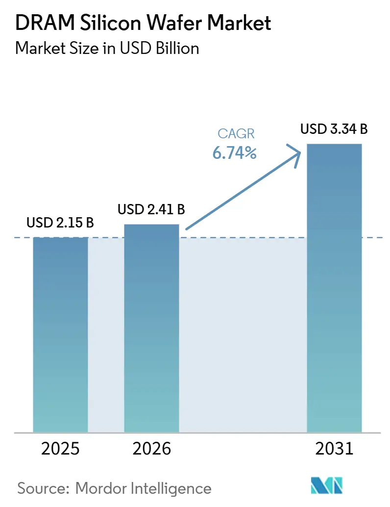
The DRAM silicon wafer market size is projected to be USD 2.15 billion in 2025, USD 2.41 billion in 2026, and reach USD 3.34 billion by 2031, growing at a CAGR of 6.74% from 2026 to 2031. Demand is being reshaped by a memory mix that now places far more weight on HBM and advanced DRAM nodes, which consume qualified 300mm wafer capacity faster than conventional DRAM products and keep effective supply tight even as installed capacity rises. The market is also supported by the broader AI infrastructure cycle, as memory makers, wafer suppliers, and equipment vendors are prioritizing advanced-node output, long-term supply commitments, and substrate quality over simple volume growth. This has strengthened pricing discipline for leading wafer suppliers, especially where customer relationships depend on long qualification cycles and consistent defect control rather than spot transactions. Public incentives in the United States, South Korea, and Japan are widening the future supply map, but these projects still need construction, ramp-up, and customer approval time before they can materially ease commercial tightness. The result is a market with high demand visibility, slow supply response, and a competitive structure that continues to favor scale, process precision, and established customer approval histories.
Key Report Takeaways
- By wafer diameter, 300mm held 86.43% of the DRAM silicon wafer market share in 2025 and is projected to expand at a 7.32% CAGR through 2031.
- By wafer type, polished wafers accounted for 94.28% of the DRAM silicon wafer market size in 2025, while epitaxial wafers are projected to expand at a 7.51% CAGR through 2031.
- By DRAM type, standard DRAM held 28.14% share in 2025, while server DRAM is projected to expand at 7.26% CAGR through 2031.
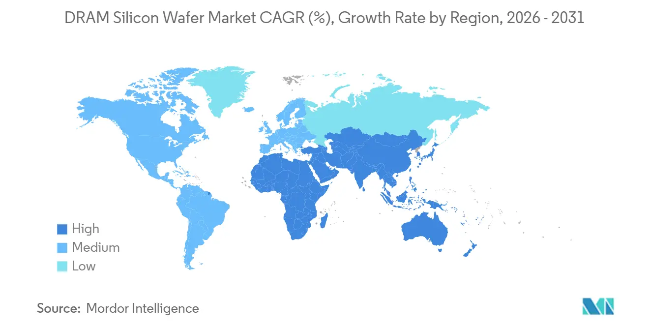
- By geography, Asia-Pacific held 78.64% share in 2025, while North America is projected to grow at 8.18% CAGR through 2031.
Note: Market size and forecast figures in this report are generated using Mordor Intelligence’s proprietary estimation framework, updated with the latest available data and insights as of January 2026.
Market Trends and Insights
Drivers Impact Analysis of DRAM Silicon Wafer Market*
| Driver | (~) % Impact on CAGR Forecast | Geographic Relevance | Impact Timeline |
|---|---|---|---|
| Rising Demand for HBM and Advanced DRAM Nodes | +2.1% | South Korea, Japan, Taiwan | Short term (≤ 2 years) |
| AI and Data Center Memory Expansion | +1.9% | Global, with a concentration in North America and the Asia-Pacific | Medium term (2-4 years) |
| 300mm Migration for Memory-Intensive Substrates | +1.3% | Global, with spillover to North America and Europe | Medium term (2-4 years) |
| Government Incentives for Domestic Wafer Supply Chains | +0.8% | North America, South Korea, Japan | Long term (≥ 4 years) |
| Tight Process Control Requirements for DRAM Yield and Uniformity | +0.5% | Japan, South Korea, Taiwan | Short term (≤ 2 years) |
| Supply Localization in Specialty Wafer Flows | +0.4% | North America, Europe | Long term (≥ 4 years) |
| Source: Mordor Intelligence | |||
Rising Demand for HBM And Advanced DRAM Nodes
The DRAM silicon wafer market is being driven by stronger demand for HBM and advanced DRAM nodes, as these products require tighter process control, more consistent starting material, and dependable access to premium 300mm polished wafers across longer production runs. SEMI reported that global silicon wafer shipments rose 5.8% in 2025 to 12,973 MSI, with polished wafer demand linked to HBM and advanced epitaxial wafer demand linked to logic as the main volume drivers behind the recovery. That product split matters for substrate suppliers because advanced memory programs now absorb a larger share of qualified capacity, leaving less room for flexible allocation across standard DRAM lines. Korea JoongAng Daily reported in May 2026 that Samsung accelerated construction of its P6 chip plant in Pyeongtaek because demand showed no sign of easing, which reinforces the continued pull from advanced memory programs across the regional supply chain. In the DRAM silicon wafer market, this keeps customer attention fixed on the timely delivery of high-quality substrates rather than on nominal fab counts alone, because the qualified wafer pool remains the real constraint.
AI and Data Center Memory Expansion
The DRAM silicon wafer market is also benefiting from AI data center build-outs, which are lifting demand across both HBM products and large-capacity server memory, broadening the number of wafer-intensive memory programs moving through the supply chain. SEMI estimated that front-end equipment spending will reach USD 133 billion in 2026, while memory equipment spending alone will rise 13% in the same year, indicating how strongly capital is being directed toward advanced semiconductor capacity. This spending pattern matters because it shows that AI infrastructure is not pulling on only one memory product family, but instead reinforcing a larger investment cycle that spans wafer demand, tool demand, and qualification activity. The Semiconductor Industry Association stated that US chip companies purchase USD 13.5 billion in silicon wafers annually, and that this figure is expected to reach USD 18.3 billion by 2029, highlighting the growing economic weight of substrate availability for future semiconductor output.[1] In the DRAM silicon wafer market, broader AI server deployment supports stronger order visibility across both standard polished wafers and more advanced substrate grades, as memory procurement is broadening rather than narrowing to a single device type.
300mm Migration for Memory-Intensive Substrates
The DRAM silicon wafer market continues to move toward 300mm substrates because advanced DRAM nodes are not economical on smaller diameters, and the production ecosystem for modern memory has become deeply optimized around 12-inch process tools and yield learning. SUMCO said 300mm wafer demand grew 9% in 2025 and pointed to continued momentum in advanced DRAM and logic applications through 2026, which confirms that the demand shift is still active rather than complete. SEMI also reported that worldwide silicon wafer shipments increased 13.1% year over year in Q1 2026 to 3,275 MSI, with advanced memory and logic leading the rebound in industry shipments. Siltronic closed its SD line for wafers up to 150mm during 2025, indicating that suppliers are retiring legacy diameter capacity rather than rebuilding it and directing attention toward larger-diameter lines that better fit the current demand mix. This leaves the DRAM silicon wafer market even more centered on 300mm platforms, where scale, qualification history, and tight defect control increasingly decide revenue, customer preference, and long-term capacity value.
Government Incentives for Domestic Wafer Supply Chains
The DRAM silicon wafer market is also being shaped by public funding programs aimed at localizing strategic wafer supply and reducing dependence on a narrow cross-border production corridor for advanced silicon materials. NIST awarded up to USD 406 million to GlobalWafers America and MEMC LLC in December 2024 to support USD 4 billion in planned 300mm silicon wafer investments in Texas and Missouri, which marked one of the clearest efforts to build domestic substrate scale in the United States. Seoul Economic Daily reported that South Korea's National Growth Fund backed SK Siltron's KRW 2.3 trillion (USD 1.59 billion), with the new 12-inch fab in Gumi targeting full-scale operations from July 2026. Shin-Etsu Chemical's 2025 annual report also highlighted the importance of Japan's domestic semiconductor support framework, in which local wafer production remains closely linked to national efforts to strengthen advanced chip supply chains. These programs will not change short-term commercial supply quickly, but they are expanding the future production map of the DRAM silicon wafer market and are making a domestic footprint a stronger competitive requirement for long-term customer agreements.
Restraints Impact Analysis of DRAM Silicon Wafer Market*
| Restraint | (~) % Impact on CAGR Forecast | Geographic Relevance | Impact Timeline |
|---|---|---|---|
| Capital Intensity of 300mm Wafer Expansion | -0.9% | Global, concentrated in Japan, South Korea, Germany, and the United States | Medium term (2-4 years) |
| Feedstock and High-Purity Polysilicon Dependency | -0.7% | Global, concentrated in East Asia for ultra-high-purity polysilicon | Long term (≥ 4 years) |
| Qualification Risk and Long Customer Approval Cycles | -0.5% | Global, with outsized exposure for entrants in North America and Europe | Long term (≥ 4 years) |
| Supply Chain Volatility From Geopolitical Reallocation | -0.4% | Asia-Pacific core, with spillover to North America and Europe | Short term (≤ 2 years) |
| Source: Mordor Intelligence | |||
Capital Intensity of 300mm Wafer Expansion
The DRAM silicon wafer market still faces a hard supply ceiling because 300mm expansion is expensive, takes years to ramp, and burdens suppliers with heavy depreciation before new lines contribute fully to earnings or cash generation. Siltronic said its new 300mm fab in Singapore added EUR 343 million (USD 388 million) to 2025 depreciation, pushing full-year EBIT to EUR -26 million (USD -29 million) even though revenue stayed flat, showing how long the payback cycle can be for new wafer capacity. SUMCO also reported a JPY 5.3 billion (USD 34 million) operating loss in Q1 2026, equivalent to, and tied that pressure mainly to higher depreciation from earlier capital spending rather than to a collapse in end demand. Suppliers therefore absorb years of costs before new output becomes commercially efficient, which slows the pace at which new investment can ease tightness in customer shipments, pricing, and contract allocation. For the DRAM silicon wafer market, capital intensity is a direct restraint because it limits fast supply response even when order visibility is strong, and buyers are willing to commit to longer agreements.
Feedstock and High-Purity Polysilicon Dependency
The DRAM silicon wafer market also remains exposed to feedstock concentration, as semiconductor-grade polysilicon is difficult to scale, purify, and qualify to the strict standards required for advanced memory wafers. The OECD said 85% of solar-grade polysilicon supply originates in China, while semiconductor-grade supply still depends heavily on East Asian processing infrastructure, leaving the broader supply chain vulnerable to regional concentration risks. NIST awarded Hemlock Semiconductor up to USD 325 million in January 2025 to build new semiconductor-grade polysilicon capacity in Michigan, which shows that upstream diversification has become a strategic infrastructure priority rather than a routine sourcing decision. The Semiconductor Industry Association warned in August 2025 that any disruption in semiconductor-grade polysilicon availability would directly affect wafer production across all diameter classes, making feedstock security a direct operating issue for downstream wafer supply. This leaves the DRAM silicon wafer market exposed to input cost swings and supply security concerns even when customer order books remain healthy and advanced memory demand continues to expand.
*Our forecasts treat driver/restraint impacts as directional, not additive. The impact forecasts reflect baseline growth, mix effects, and variable interactions.
DRAM Silicon Wafer Market Segment Analysis
By Wafer Diameter:
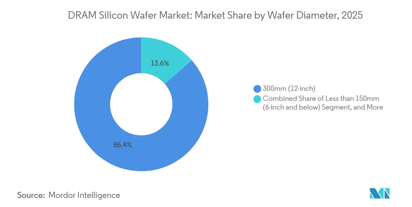
300mm Substrates Define Capacity PrioritiesThe 300mm segment held 86.43% of the DRAM silicon wafer market share in 2025, making it the clear center of demand, investment planning, and customer qualification activity across the supply chain. It leads because advanced DRAM cells require tight lithography, strong yield control, and a mature process infrastructure, which are only economical at the 300mm scale for commercial production at leading nodes. SUMCO said 300mm wafer demand grew 9% in 2025 and pointed to continued momentum in advanced DRAM applications through 2026, which supports the view that the largest-diameter class is still gaining practical importance in current customer programs.[2] SEMI reported that worldwide silicon wafer shipments increased 13.1% year over year in Q1 2026 to 3,275 MSI, with advanced memory and logic leading the recovery, and that aligns closely with the demand profile that favors 300mm substrate consumption.
Smaller diameters remain tied to specialty and legacy uses, so they do not compete at scale for advanced DRAM programs and do not materially alter where the main commercial value of the DRAM silicon wafer market is being created. Siltronic said customer inventories remained elevated outside AI-linked applications in early 2026, indicating weaker conditions for non-advanced wafer demand and underlining the widening gap between advanced and legacy-diameter economics. The company also closed its SD line for wafers up to 150mm in 2025, reinforcing that legacy diameter capacity is being retired rather than renewed as suppliers reshape their portfolios around more relevant substrate classes. In the DRAM silicon wafer market, wafer diameter now works as a clear proxy for node generation because 300mm aligns with advanced DRAM while smaller formats sit at the edge of the category and attract far less strategic investment.

By Wafer Type:
Epitaxial Wafers Gain Ground as Node Control TightensPolished wafers accounted for 94.28% of the DRAM silicon wafer market in 2025, underscoring how firmly current HBM3E and mainstream DRAM production still rely on standard prime-polished material that has long been qualified in high-volume memory lines. The segment remains dominant because current production programs already have deep qualification histories, long-term contracts, and stable operating recipes built around polished 300mm wafers that customers can scale reliably. SEMI said polished wafer demand tied to HBM was one of the main drivers of the 2025 shipment recovery, confirming that polished substrates remain central to the current growth cycle rather than being displaced by a new wafer format. That keeps polished substrates at the core of current revenue and operating volume, even as customers begin to demand tighter control over starting materials at the most advanced nodes.
Epitaxial wafers are the fastest-growing wafer type and are projected to expand at 7.51% CAGR through 2031, reflecting rising sensitivity to contamination control, resistivity stability, and defect density at leading-edge DRAM nodes where process margins are narrower. SEMI also pointed to strong advanced-epitaxial wafer demand in logic during 2025, indicating that epi capability is already becoming a broader differentiator across advanced semiconductor manufacturing and is no longer a niche technical feature. For suppliers that can serve both formats, the product mix is shifting toward a higher-value portfolio while polished wafers continue to set the baseline shipment volume of the DRAM silicon wafer market across current memory output. This means polished wafers will likely keep the largest base through the forecast period, while epi gains share in the most demanding process flows where yield sensitivity and material consistency matter most.
By DRAM Type:
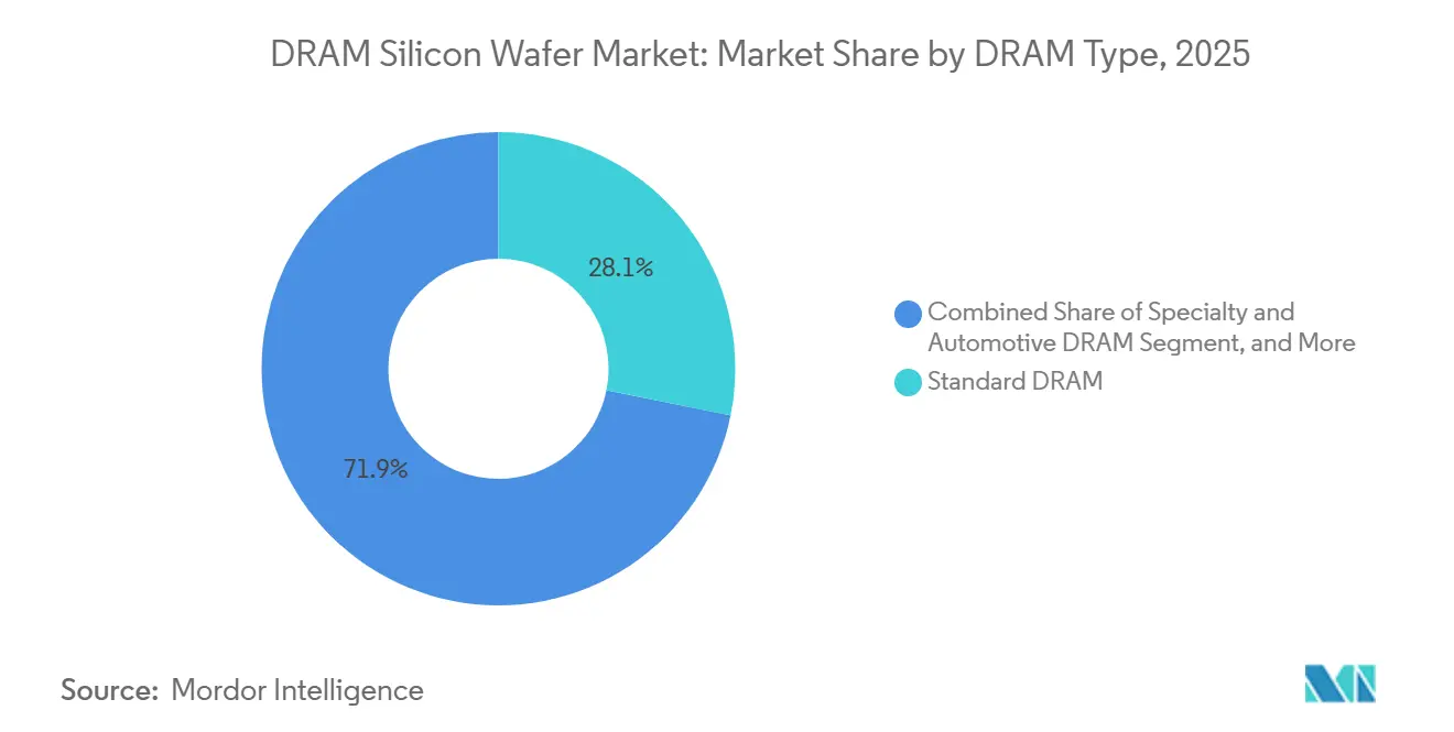
Server DRAM Leads Growth While Standard DRAM Holds the Largest BaseStandard DRAM held a 28.14% share in 2025, making it the largest base in the DRAM silicon wafer market, even after AI memory demand accelerated and redirected industry attention toward premium products. Its position reflects the scale of PC and consumer electronics demand, which still uses a meaningful share of mature-node wafer capacity and keeps standard DRAM relevant to capacity planning across large parts of the supply chain. Server DRAM is projected to expand at a 7.26% CAGR through 2031, as hyperscalers add high-capacity DDR5 RDIMMs alongside HBM in AI server platforms and increase demand for memory products that fall outside the narrow HBM category. This gives the DRAM silicon wafer market two simultaneous growth layers, one tied to premium HBM products and another tied to large-volume server memory, which together stretch demand across the same advanced substrate pool.
Mobile DRAM plays a large role because LPDDR platforms remain central to premium smartphones and edge AI devices, thereby preserving a steady base of memory-related wafer pull outside the data center build-out cycle. Graphics DRAM is also benefiting from newer GPU launches, which are pushing wafer demand toward tighter process nodes and are supporting another pocket of advanced memory-related substrate use. Specialty and automotive DRAM add stability because qualification cycles are long, design-win periods are extended, and approved programs are harder to interrupt once supply is accepted into vehicle and industrial electronics systems. As a result, the DRAM silicon wafer market draws demand from both fast-growing server applications and steadier end uses that help smooth the cycle when individual memory categories move at different speeds.
Geography Analysis
South Korea and Japan DRAM Silicon Wafer Market
Asia-Pacific held 78.64% of the DRAM silicon wafer market share in 2025, so the region remained the clear operating center of the category and the main corridor linking substrate supply with advanced memory fabrication. South Korea sits at the core of that position because Samsung Electronics and SK Hynix anchor the global base for advanced DRAM and HBM production, giving the country an outsized role in pulling qualified wafer supply through multi-year customer programs. Korea JoongAng Daily reported that Samsung's Pyeongtaek P5 and fast-tracked P6 complex are expected to reach a combined 600,000 wafers per month, pointing to another large increase in memory-linked substrate demand from the same geography. Japan strengthens the same corridor because Shin-Etsu Handotai and SUMCO together supply more than half of the global 300mm wafer volume, linking Japanese wafer output closely with South Korean memory production and keeping the region highly interdependent.
North America DRAM Silicon Wafer Market
North America is projected to grow at 8.18% CAGR through 2031, making it the fastest-growing regional slice of the DRAM silicon wafer market and the clearest example of supply localization moving from policy into physical capacity. This shift is being driven by CHIPS Act support for local wafer supply, which had been largely absent at advanced commercial 300mm scale in the United States before the current investment cycle began. NIST said GlobalWafers America and MEMC LLC received up to USD 406 million in direct funding to support USD 4 billion in Texas and Missouri wafer investments, which gives the region a stronger foundation for domestic substrate sourcing.[3] The Sherman, Texas project is positioned as the first advanced high-volume 300mm silicon wafer plant in the United States, which matters because it brings memory and logic customers closer to local starting material supply. The Semiconductor Industry Association's projection that US silicon wafer purchases will reach USD 18.3 billion by 2029 explains why domestic buyers are pushing for a broader and more resilient supply base.
Europe and China DRAM Silicon Wafer Market
Europe remains more concentrated around specialty-grade wafer production and process research than around new greenfield scale, which keeps it relevant to technology depth but less central to near-term capacity share gains in the DRAM silicon wafer market. Siltronic said its Singapore fab entered depreciation in August 2025 and that 2026 revenue would face pressure from exchange rates, the SD line closure, and inventory corrections outside the strongest AI-linked markets, which shows that European-linked suppliers are still balancing advanced growth with weaker legacy exposure. China is also trying to deepen regional self-sufficiency, with Nikkei Asia reporting a policy target for domestic chipmakers to source more than 70% of their silicon wafers from Chinese suppliers by the end of 2026, which supports local expansion plans even under pricing pressure. Across the DRAM silicon wafer market, geography is therefore shifting from a single Asia-led production corridor toward a broader but still highly concentrated map where domestic supply goals are rising faster than qualified new capacity.
Competitive Landscape
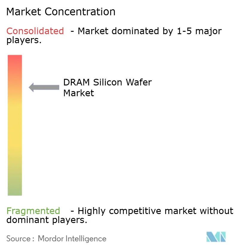
The DRAM silicon wafer market remains highly concentrated, with Shin-Etsu Handotai, SUMCO Corporation, GlobalWafers, Siltronic AG, and SK Siltron controlling 90% of global 300mm prime-polished capacity, leaving only limited room for smaller suppliers to influence the top end of the commercial supply. That level of concentration gives leading suppliers strong influence over qualification timing, contract structure, and capacity allocation across memory customers that need stable wafer quality and dependable delivery over long approval cycles. The competitive edge of the top group comes from crystal growth quality, defect control, and the ability to deliver steady output across advanced-node requirements that customers cannot switch easily without operational risk. In the DRAM silicon wafer market, this keeps scale, process discipline, and long customer history more important than simple nameplate expansion alone.
Strategic investment remained the main competitive pattern in 2025 and 2026, as suppliers and memory makers moved to secure future wafer availability rather than rely on short-term purchasing flexibility. Siltronic continued ramping its Singapore 300mm fab, even though the heavier depreciation burden weighed on near-term earnings, underscoring how strongly the company is leaning into future advanced-wafer demand despite near-term financial pressure.[4] GlobalWafers advanced its Texas project with federal support, giving it a direct route into a new domestic sourcing position for US semiconductor customers that want a local high-volume 300mm supplier. SK Siltron also pushed ahead with its Gumi expansion, backed by South Korea's National Growth Fund, to raise 12-inch output from July 2026 onward and strengthen its role inside the regional memory supply chain. These moves show that competition in the DRAM silicon wafer market is centered on who can bring qualified 300mm capacity online fastest without compromising defect performance, customer trust, or operating discipline.
Chinese suppliers remain the most active challengers because policy support is encouraging local wafer expansion and consolidation, even though closing the technical and qualification gap will take longer than adding headline capacity. Nikkei Asia reported that China wanted domestic chipmakers to source more than 70% of their silicon wafers from Chinese suppliers by the end of 2026, which gives NSIG and related local players a clear domestic target for expansion and customer capture. Even so, new entrants still face strict standards for flatness, purity, nanotopography, and uniformity, and they must pass multi-year qualification cycles before they can materially change commercial share in advanced memory supply. The DRAM silicon wafer market therefore remains oligopolistic today, even as regional challengers work to narrow the gap through policy-backed scale-up, portfolio consolidation, and longer customer engagement.
DRAM Silicon Wafer Industry Leaders
-
Shin-Etsu Handotai Co., Ltd.
-
SUMCO Corporation
-
GlobalWafers Co., Ltd.
-
Siltronic AG
-
SK Siltron Co., Ltd.
- *Disclaimer: Major Players sorted in no particular order
DRAM Silicon Wafer Market Companies Covered in this Report
- Shin-Etsu Handotai Co., Ltd.
- SUMCO Corporation
- GlobalWafers Co., Ltd.
- Siltronic AG
- SK Siltron Co., Ltd.
- Soitec S.A.
- Okmetic Oyj
- Wafer Works Corporation
- RS Technologies Co., Ltd.
- Topsil Semiconductor Materials A/S
- Shanghai Simgui Technology Co., Ltd.
- National Silicon Industry Group Co., Ltd.
- GRINM Semiconductor Materials Co., Ltd.
- Zhejiang Jinruihong Technology Co., Ltd.
- Hangzhou Semiconductor Wafer Co., Ltd.
- Zhonghuan Advanced Semiconductor Materials Co., Ltd.
- FST Corporation
Recent Industry Developments in DRAM Silicon Wafer Market
- May 2026: Korea Development Bank and Woori Bank arranged KRW 2.5 trillion (USD 1.72 billion) in acquisition financing for Doosan Group's planned takeover of a 70.6% stake in SK Siltron from SK Inc., valuing the company at KRW 5 trillion (USD 3.45 billion). The financing underscored South Korea's state-backed interest in preserving its semiconductor wafer supply chain.
- April 2026: SEMI reported that worldwide silicon wafer shipments increased 13.1% year over year in Q1 2026, reaching 3,275 MSI, driven by strong demand for AI data center applications, including advanced logic, HBM, and increasingly power management devices, while sequential demand declined 4.7% in line with typical seasonality.
- February 2026: SK hynix's board approved an investment of KRW 21.61 trillion (USD 15.7 billion) to construct phases 2 through 6 of its first fabrication plant complex at the Yongin Semiconductor Cluster, running from March 2026 through December 2030, with production dedicated to HBM and advanced DRAM.
- February 2026: SEMI reported that global silicon wafer shipments rose 5.8% in 2025 to 12,973 MSI, with the year marking an inflection point as HBM polished wafer demand and advanced logic epitaxial wafer demand returned volumes to growth. Wafer revenue declined 1.2% to USD 11.4 billion because conventional semiconductor pricing remained soft.
Global DRAM Silicon Wafer Market Report Scope
The DRAM silicon wafer market encompasses the production, supply, and use of silicon wafers specifically designed for the manufacture of dynamic random-access memory (DRAM) chips. The scope includes wafers used across DRAM fabrication processes for applications in consumer electronics, data centers, automotive systems, industrial equipment, and other memory-intensive end-user industries.
The DRAM Silicon Wafer Market Report is Segmented by Wafer Diameter (300mm [12-Inch], 200mm [8-Inch], and less than 150mm [6-Inch and Below]), Wafer Type (Polished Wafers, and Epitaxial [Epi] Wafers), DRAM Type (Standard DRAM, Mobile DRAM [LPDDR], Graphics DRAM [GDDR], Server DRAM, and Specialty and Automotive DRAM), and Geography (North America, Europe, Asia-Pacific, and Rest of the World). The Market Forecasts are Provided in Terms of Value (USD).
Segmentation Overview
| 300mm (12-inch) |
| 200mm (8-inch) |
| Less than 150mm (6-inch and below) |
| Polished Wafers |
| Epitaxial (Epi) Wafers |
| Standard DRAM |
| Mobile DRAM (LPDDR) |
| Graphics DRAM (GDDR) |
| Server DRAM |
| Specialty and Automotive DRAM |
| North America | |
| Europe | |
| Asia-Pacific | China |
| Japan | |
| South Korea | |
| Taiwan | |
| Rest of Asia-Pacific | |
| Rest of the World |
| By Wafer Diameter | 300mm (12-inch) | |
| 200mm (8-inch) | ||
| Less than 150mm (6-inch and below) | ||
| By Wafer Type | Polished Wafers | |
| Epitaxial (Epi) Wafers | ||
| By DRAM Type | Standard DRAM | |
| Mobile DRAM (LPDDR) | ||
| Graphics DRAM (GDDR) | ||
| Server DRAM | ||
| Specialty and Automotive DRAM | ||
| By Geography | North America | |
| Europe | ||
| Asia-Pacific | China | |
| Japan | ||
| South Korea | ||
| Taiwan | ||
| Rest of Asia-Pacific | ||
| Rest of the World | ||
Key Questions Answered in the Report
What is the current size and forecast for the DRAM silicon wafer market?
The DRAM silicon wafer market was valued at USD 2.15 billion in 2025, is valued at USD 2.41 billion in 2026, and is forecast to reach USD 3.34 billion by 2031 at a CAGR of 6.74% over 2026-2031.
Which wafer diameter leads demand in DRAM silicon wafer production?
The 300mm segment led with 86.43% share in 2025 because advanced DRAM nodes depend on 12-inch process economics, mature tool ecosystems, and higher-yield manufacturing.
Which wafer type is expanding fastest in this space?
Epitaxial wafers are projected to grow at 7.51% CAGR through 2031, while polished wafers still held the dominant 94.28% share in 2025 because they remain the base format for current high-volume memory output.
Which DRAM product category is growing fastest?
Server DRAM is projected to expand at 7.26% CAGR through 2031 as hyperscalers add more DDR5 RDIMMs alongside HBM in AI server deployments, even though standard DRAM remained the largest category in 2025.
Which region dominates, and which region is growing fastest?
Asia-Pacific dominated with 78.64% share in 2025 because it combines South Korean memory fabs with major Japanese wafer suppliers, while North America is the fastest-growing region at 8.18% CAGR through 2031 due to CHIPS Act-backed localization.
Why does supply remain tight even with new investment announcements?
Supply remains tight because 300mm fabs take years to build and qualify, depreciation burdens are heavy during ramp-up, semiconductor-grade polysilicon is concentrated, and the qualified supplier base is still controlled by a small group of large incumbents.